ICGOO在线商城 > 集成电路(IC) > 数据采集 - 模数转换器 > AD7693BCPZRL7
 Datasheet下载
- 型号: AD7693BCPZRL7
- 制造商: Analog
- 库位|库存: xxxx|xxxx
- 要求:
| 数量阶梯 | 香港交货 | 国内含税 |
| +xxxx | $xxxx | ¥xxxx |
查看当月历史价格
查看今年历史价格
AD7693BCPZRL7产品简介:
ICGOO电子元器件商城为您提供AD7693BCPZRL7由Analog设计生产,在icgoo商城现货销售,并且可以通过原厂、代理商等渠道进行代购。 AD7693BCPZRL7价格参考。AnalogAD7693BCPZRL7封装/规格:数据采集 - 模数转换器, 16 Bit Analog to Digital Converter 1 Input 1 SAR 10-LFCSP-WD(3x3)。您可以下载AD7693BCPZRL7参考资料、Datasheet数据手册功能说明书,资料中有AD7693BCPZRL7 详细功能的应用电路图电压和使用方法及教程。
AD7693BCPZRL7是Analog Devices Inc.推出的一款18位、逐次逼近型模数转换器(SAR ADC),具有高精度、低功耗和小封装的特点,适用于对信号精度要求较高的工业与测量场景。该器件采用2.5V参考电压时可实现优异的信噪比(SNR)和积分非线性(INL),支持单通道真差分输入,采样速率达250 kSPS。

其典型应用场景包括:工业自动化中的高精度传感器信号采集,如压力、温度、流量等传感器的模拟信号转换;便携式仪器仪表,如数据记录仪、手持式测试设备,得益于其低功耗特性,适合电池供电系统;医疗设备中用于生物电信号(如心电、脑电)的采集处理;以及精密数据采集系统(DAQ)、过程控制和PLC模块等。

AD7693BCPZRL7采用小型化6引脚SOT-23封装,节省PCB空间,便于在紧凑型设计中集成。同时,它具备出色的直流和交流性能,能够在宽温度范围(-40°C至+125°C)稳定工作,适应严苛工业环境。通过SPI兼容串行接口与主控芯片通信,易于系统集成。

综上,AD7693BCPZRL7广泛应用于需要高分辨率、低噪声和可靠性的中速数据采集场合,是工业测量、医疗监测和精密仪器中的理想ADC选择。
| 参数 | 数值 |
| 产品目录 | 集成电路 (IC) |
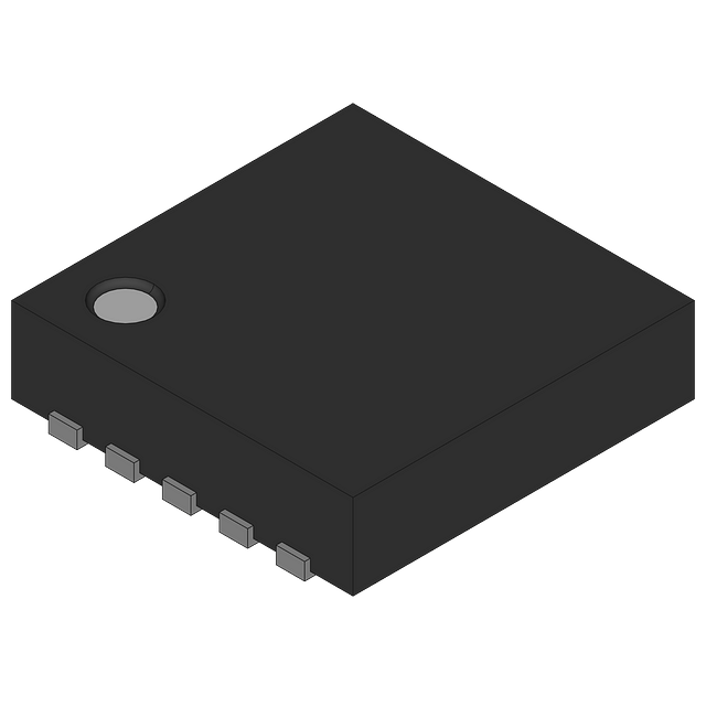
| 描述 | IC ADC 16BIT 500KSPS 10-LFCSP |
| 产品分类 | |
| 品牌 | Analog Devices Inc |
| 数据手册 | |
| 产品图片 |
|
| 产品型号 | AD7693BCPZRL7 |
| rohs | 无铅 / 符合限制有害物质指令(RoHS)规范要求 |
| 产品系列 | PulSAR® |
| 位数 | 16 |
| 供应商器件封装 | 10-LFCSP-WD(3x3) |
| 其它名称 | AD7693BCPZRL7DKR |
| 包装 | Digi-Reel® |
| 安装类型 | 表面贴装 |
| 封装/外壳 | 10-WFDFN 裸露焊盘,CSP |
| 工作温度 | -40°C ~ 85°C |
| 数据接口 | DSP,MICROWIRE™,QSPI™,串行,SPI™ |
| 标准包装 | 1 |
| 特性 | - |
| 电压源 | 模拟和数字 |
| 转换器数 | 1 |
| 输入数和类型 | 1 个差分,双极 |
| 配用 | /product-detail/zh/EVAL-AD7693-PMDZ/EVAL-AD7693-PMDZ-ND/4875928 |
| 采样率(每秒) | 500k |


- 商务部:美国ITC正式对集成电路等产品启动337调查
- 曝三星4nm工艺存在良率问题 高通将骁龙8 Gen1或转产台积电
- 太阳诱电将投资9.5亿元在常州建新厂生产MLCC 预计2023年完工
- 英特尔发布欧洲新工厂建设计划 深化IDM 2.0 战略
- 台积电先进制程称霸业界 有大客户加持明年业绩稳了
- 达到5530亿美元!SIA预计今年全球半导体销售额将创下新高
- 英特尔拟将自动驾驶子公司Mobileye上市 估值或超500亿美元
- 三星加码芯片和SET,合并消费电子和移动部门,撤换高东真等 CEO
- 三星电子宣布重大人事变动 还合并消费电子和移动部门
- 海关总署:前11个月进口集成电路产品价值2.52万亿元 增长14.8%


PDF Datasheet 数据手册内容提取
16-Bit, ±0.5 LSB, 500 kSPS PulSAR® Differential ADC in MSOP Data Sheet AD7693 FEATURES APPLICATION DIAGRAM 16-bit resolution with no missing codes +2.5VTO +5V +5V Throughput: 500 kSPS INL/DNL: ±0.25 LSB typ, ±0.5 LSB max (±8 ppm of FSR) Dynamic range: 96.5 dB REF VDDVIO +1.8VTO VDD SINAD: 96 dB at 1 kHz IN+ SDI AD7693 SCK 3- OR 4-WIRE THD: −120 dB at 1 kHz ±10V, ±5V, ... IN– SDO (ISNPTIE, DRAFAISCYE CHAIN, CS) Tru0e V d tioff VerReEFn wtiiatlh a VnRaElFo ugp i ntop VuDt rDa nogne b: o±tVhR EinF puts ADA4941-1 GND CNV 06394-002 Figure 2. No pipeline delay Single-supply 5 V operation with Table 1. MSOP 14-/16-/18-Bit PulSAR ADC 1.8 V/2.5 V/3 V/5 V logic interface 400 kSPS Proprietary serial interface 100 250 to ADC SPI®-/QSPI™-/MICROWIRE™-/DSP-compatible1 Type kSPS kSPS 500 kSPS Driver Daisy-chain multiple ADCs, selectable busy indicator 18-Bit AD7691 AD7690 ADA4941-1, ADA4841-2 Power dissipation: 40 nJ/conversion 40 μW at 5 V/1 kSPS 16-Bit True AD7684 AD7687 AD7688, ADA4941-1, Differential AD7693 ADA4841-2 4 mW at 5 V/100 kSPS 16-Bit Pseudo AD7683 AD7685 AD7686 ADA4841-1 18 mW at 5 V/500 kSPS Differential/ AD7680 AD7694 Standby current: 1 nA Unipolar 10-lead package: MSOP (MSOP-8 size) 14-Bit AD7940 AD7942 AD7946 ADA4841-1, Pin-for-pin compatible with the 16-bit AD7687 and AD7688 ADA4841-2 and the 18-bit AD7690 and AD7691 APPLICATIONS GENERAL DESCRIPTION Battery-powered equipment The AD7693 is a 16-bit, successive approximation analog-to- Data acquisitions digital converter (ADC) that operates from a single power supply, Seismic data acquisition systems VDD. It contains a low power, high speed, 16-bit sampling ADC DVMs with no missing codes, an internal conversion clock, and a Instrumentation versatile serial interface port. The reference voltage, VREF, is Medical instruments applied externally and can be set up to the supply voltage, VDD. On the CNV rising edge, it samples the voltage difference 1.0 POSITIVE INL = +0.17LSB between the IN+ and IN− pins. The voltages on these pins NEGATIVE INL = –0.17LSB 0.8 swing in opposite phase between 0 V and V about V /2. REF REF 0.6 Its power scales linearly with throughput. 0.4 Using the SDI input, the SPI-compatible serial interface also B) 0.2 S features the ability to daisy-chain several ADCs on a single L (L 0 3-wire bus and provides an optional busy indicator. It is compatible N I–0.2 with 1.8 V, 2.5 V, 3 V, or 5 V logic, using the separate VIO supply. –0.4 The AD7693 is housed in a 10-lead MSOP with operation –0.6 specified from −40°C to +85°C. –0.8 –1.00 16384 C32O7D6E8 49152 65536 06394-001 1 Protected by U.S. Patent 6,703,961. Figure 1. Integral Nonlinearity vs. Code Rev. C Document Feedback Information furnished by Analog Devices is believed to be accurate and reliable. However, no responsibility is assumed by Analog Devices for its use, nor for any infringements of patents or other One Technology Way, P.O. Box 9106, Norwood, MA 02062-9106, U.S.A. rights of third parties that may result from its use. Specifications subject to change without notice. No license is granted by implication or otherwise under any patent or patent rights of Analog Devices. Tel: 781.329.4700 ©2006–2019 Analog Devices, Inc. All rights reserved. Trademarks and registered trademarks are the property of their respective owners. Technical Support www.analog.com
AD7693 Data Sheet TABLE OF CONTENTS Features .............................................................................................. 1 Driver Amplifier Choice ........................................................... 14 Applications ....................................................................................... 1 Single-Ended-to-Differential Driver ....................................... 15 Application Diagram ........................................................................ 1 Voltage Reference Input ............................................................ 15 General Description ......................................................................... 1 Power Supply ............................................................................... 15 Revision History ............................................................................... 2 Supplying the ADC from the Reference .................................. 16 Specifications ..................................................................................... 3 Digital Interface .......................................................................... 16 Timing Specifications ....................................................................... 5 CS Mode, 3-Wire Without Busy Indicator ............................. 17 Absolute Maximum Ratings ............................................................ 6 CS Mode, 3-Wire with Busy Indicator .................................... 18 ESD Caution .................................................................................. 6 CS Mode, 4-Wire Without Busy Indicator ............................. 19 Pin Configurations and Function Descriptions ........................... 7 CS Mode, 4-Wire with Busy Indicator .................................... 20 Terminology ...................................................................................... 8 Chain Mode Without Busy Indicator ...................................... 21 Typical Performance Characteristics ............................................. 9 Chain Mode with Busy Indicator ............................................. 22 Theory of Operation ...................................................................... 12 Application Hints ........................................................................... 23 Circuit Information .................................................................... 12 Layout .......................................................................................... 23 Converter Operation .................................................................. 12 Evaluating the AD7693 Performance ...................................... 23 Typical Connection Diagram ................................................... 13 Outline Dimensions ....................................................................... 24 Analog Inputs .............................................................................. 14 Ordering Guide .......................................................................... 24 REVISION HISTORY 6/2019—Rev. B to Rev. C 6/2011—Rev. 0 to Rev. A Deleted LFCSP .................................................................... Universal Changes to Resolution Parameter and Common-Mode Input Changes to Features Section and General Range Parameter in Table 2 .............................................................. 3 Description Section .......................................................................... 1 Changes to Figure 6 and Table 6 ...................................................... 7 Changes to Absolute Maximum Ratings Section ......................... 6 Updated Outline Dimensions ....................................................... 24 Deleted Figure 6; Renumbered Sequentially ................................. 7 Changes to Ordering Guide .......................................................... 24 Changes to Table 6 ............................................................................ 7 Changes to Circuit Information Section ..................................... 12 12/2006—Revision 0: Initial Version Changes to Table 8 .......................................................................... 15 Change to Layout Section .............................................................. 23 Deleted Figure 49 ............................................................................ 24 Changes to Ordering Guide .......................................................... 24 6/2014—Rev. A to Rev. B Added Patent Footnote .................................................................... 1 Changes to Evaluating the AD7693 Performance Section ........ 23 Updated Outline Dimensions (Dimensions Not Changed; Lead-to-Pad Dimensions Updated for JEDEC Compliance) ... 24 Changes to Ordering Guide .......................................................... 24 Rev. C | Page 2 of 24
Data Sheet AD7693 SPECIFICATIONS VDD = 4.5 V to 5.5 V, VIO = 2.3 V to VDD, V = VDD, all specifications T to T , unless otherwise noted. REF MIN MAX Table 2. Parameter Conditions/Comments Min Typ Max Unit RESOLUTION 16 Bits ANALOG INPUT Voltage Range IN+ − (IN−) −V +V V REF REF Absolute Input Voltage IN+, IN− −0.1 V + 0.1 V REF Common-Mode Input Range IN+, IN− V /2 – 0.1 V /2 V /2 + 0.1 V REF REF REF Analog Input CMRR f = 250 kHz 65 dB IN Leakage Current at 25°C Acquisition phase 1 nA Input Impedance1 THROUGHPUT Conversion Rate 0 500 kSPS Transient Response Full-scale step 400 ns ACCURACY No Missing Codes 16 Bits Integral Linearity Error −0.5 ±0.25 +0.5 LSB2 Differential Linearity Error −0.5 ±0.25 +0.5 LSB Transition Noise REF = VDD = 5 V 0.35 LSB Gain Error3 −20 ±0.5 +20 LSB Gain Error Temperature Drift ±0.3 ppm/°C Zero Error3 −5 ±0.5 +5 LSB Zero Temperature Drift ±0.3 ppm/°C Power Supply Sensitivity VDD = 5 V 5% ±1 ppm AC ACCURACY4 Dynamic Range 96 96.5 dB5 Signal-to-Noise f = 1 kHz 95.5 96 dB IN f = 10 kHz 95.5 dB IN f = 100 kHz 93 dB IN f = 1 kHz, V = 2.5 V 93 dB IN REF Signal-to-(Noise + Distortion) f = 1 kHz 95.5 96 dB IN f = 10 kHz 95.5 dB IN f = 100 kHz 90 dB IN Total Harmonic Distortion f = 1 kHz −120 −108 dB IN f = 10 kHz −113 dB IN f = 100 kHz −92 dB IN Spurious-Free Dynamic Range f = 1 kHz 120 dB IN f = 10 kHz 114 dB IN f = 100 kHz 93.5 dB IN Intermodulation Distortion6 115 dB 1 See the Analog Inputs section. 2 LSB means least significant bit. With the ±5 V input range, one LSB is 152.6 μV. 3 See the Terminology section. These specifications include full temperature range variation but not the error contribution from the external reference. 4 With VREF = 5 V, unless otherwise noted. 5 All specifications expressed in decibels are referred to a full-scale input FSR and tested with an input signal at 0.5 dB below full scale, unless otherwise specified. 6 fIN1 = 21.4 kHz and fIN2 = 18.9 kHz, with each tone at −7 dB below full scale. Rev. C | Page 3 of 24
AD7693 Data Sheet VDD = 4.5 V to 5.5 V, VIO = 2.3 V to VDD, V = VDD, all specifications T to T , unless otherwise noted. REF MIN MAX Table 3. Parameter Conditions/Comments Min Typ Max Unit REFERENCE Voltage Range 0.5 VDD + 0.3 V Load Current 500 kSPS, REF = 5 V 100 μA SAMPLING DYNAMICS −3 dB Input Bandwidth 9 MHz Aperture Delay VDD = 5V 2.5 ns DIGITAL INPUTS Logic Levels V −0.3 +0.3 × VIO V IL V 0.7 × VIO VIO + 0.3 V IH I −1 +1 μA IL I −1 +1 μA IH DIGITAL OUTPUTS Data Format Serial 16 bits, twos complement Pipeline Delay1 V I = +500 μA 0.4 V OL SINK V I = −500 μA VIO − 0.3 V OH SOURCE POWER SUPPLIES VDD Specified performance 4. 5 5.5 V VIO Specified performance 2.3 VDD + 0.3 V VIO Range 1.8 VDD + 0.3 V Standby Current2, 3 VDD and VIO = 5 V, 25°C 1 50 nA Power Dissipation 100 SPS throughput 5 μW 100 kSPS throughput 4 mW 500 kSPS throughput 18 21.5 mW Energy per Conversion 40 nJ TEMPERATURE RANGE4 Specified Performance T to T −40 +85 °C MIN MAX 1 Conversion results available immediately after completed conversion. 2 With all digital inputs forced to VIO or GND as required. 3 During acquisition phase. 4 Contact an Analog Devices sales representative for the extended temperature range. Rev. C | Page 4 of 24
Data Sheet AD7693 TIMING SPECIFICATIONS VDD = 4.5 V to 5.5 V, VIO = 2.3 V to VDD, V = VDD, all specifications T to T , unless otherwise noted. REF MIN MAX Table 4.1 Parameter Symbol Min Typ Max Unit Conversion Time: CNV Rising Edge to Data Available t 0.5 1.6 μs CONV Acquisition Time t 400 ns ACQ Time Between Conversions t 2.0 μs CYC CNV Pulse Width (CS Mode) t 10 ns CNVH SCK Period (CS Mode) t 15 ns SCK SCK Period (Chain Mode) t SCK VIO Above 4.5 V 17 ns VIO Above 3 V 18 ns VIO Above 2.7 V 19 ns VIO Above 2.3 V 20 ns SCK Low Time t 7 ns SCKL SCK High Time t 7 ns SCKH SCK Falling Edge to Data Remains Valid t 4 ns HSDO SCK Falling Edge to Data Valid Delay t DSDO VIO Above 4.5 V 14 ns VIO Above 3 V 15 ns VIO Above 2.7 V 16 ns VIO Above 2.3 V 17 ns CNV or SDI Low to SDO D15 MSB Valid (CS Mode) t EN VIO Above 4.5 V 15 ns VIO Above 2.7 V 18 ns VIO Above 2.3 V 22 ns CNV or SDI High or Last SCK Falling Edge to SDO High Impedance (CS Mode) t 25 ns DIS SDI Valid Setup Time from CNV Rising Edge (CS Mode) t 15 ns SSDICNV SDI Valid Hold Time from CNV Rising Edge (CS Mode) t 0 ns HSDICNV SCK Valid Setup Time from CNV Rising Edge (Chain Mode) t 5 ns SSCKCNV SCK Valid Hold Time from CNV Rising Edge (Chain Mode) t 10 ns HSCKCNV SDI Valid Setup Time from SCK Falling Edge (Chain Mode) t 4 ns SSDISCK SDI Valid Hold Time from SCK Falling Edge (Chain Mode) t 4 ns HSDISCK SDI High to SDO High (Chain Mode with Busy Indicator) t DSDOSDI VIO Above 4.5 V 15 ns VIO Above 2.3 V 26 ns 1 See Figure 3 and Figure 4 for load conditions. Rev. C | Page 5 of 24
AD7693 Data Sheet ABSOLUTE MAXIMUM RATINGS Table 5. Stresses at or above those listed under Absolute Maximum Parameter Rating Ratings may cause permanent damage to the product. This is a Analog Inputs stress rating only; functional operation of the product at these IN+,1 IN−1 GND − 0.3 V to VDD + 0.3 V or any other conditions above those indicated in the operational or ±130 mA section of this specification is not implied. Operation beyond REF GND − 0.3 V to VDD + 0.3 V the maximum operating conditions for extended periods may Supply Voltages affect product reliability. VDD, VIO to GND −0.3 V to +7 V ESD CAUTION VDD to VIO ±7 V Digital Inputs to GND −0.3 V to VIO + 0.3 V Digital Outputs to GND −0.3 V to VIO + 0.3 V Storage Temperature Range −65°C to +150°C Junction Temperature 150°C θJA Thermal Impedance 200°C/W θ Thermal Impedance 44°C/W JC Lead Temperature Range JEDEC J-STD-20 1 See the Analog Inputs section. 500µA IOL TO SDO 1.4V CL 50pF 500µA IOH 06394-003 Figure 3. Load Circuit for Digital Interface Timing 70% VIO 30% VIO t t DELAY DELAY 2V OR VIO – 0.5V1 2V OR VIO – 0.5V1 0.8V OR 0.5V2 0.8V OR 0.5V2 1220V.8 VIF I FV IVOI OA BAOBVOEV E2. 52V.5,V V, I0O.5 –V 0 I.F5 VV IIOF VBIEOL OBEWL O2.W5V 2..5V. 06394-004 Figure 4. Voltage Levels for Timing Rev. C | Page 6 of 24
Data Sheet AD7693 PIN CONFIGURATIONS AND FUNCTION DESCRIPTIONS REF 1 10 VIO VDD 2 AD7693 9 SDI IN+ 3 TOP VIEW 8 SCK GINND– 45 (Not to Scale) 76 SCDNOV 06394-005 Figure 5. Pin Configuration Table 6. Pin Function Descriptions Pin No. Mnemonic Type1 Description 1 REF AI Reference Input Voltage. The REF range is from 0.5 V to VDD. It is referred to the GND pin. This pin should be decoupled closely to the pin with a 10 μF capacitor. 2 VDD P Power Supply. 3 IN+ AI Differential Positive Analog Input. 4 IN− AI Differential Negative Analog Input. 5 GND P Power Supply Ground. 6 CNV DI Convert Input. This input has multiple functions. On its leading edge, it initiates the conversions and selects the interface mode of the part: chain or CS mode. In chain mode, the data should be read when CNV is high. In CS mode, the SDO pin is enabled when CNV is low. 7 SDO DO Serial Data Output. The conversion result is output on this pin. It is synchronized to SCK. 8 SCK DI Serial Data Clock Input. When the part is selected, the conversion result is shifted out by this clock. 9 SDI DI Serial Data Input. This input provides multiple features. It selects the interface mode of the ADC as follows: Chain mode is selected if SDI is low during the CNV rising edge. In this mode, SDI is used as a data input to daisy-chain the conversion results of two or more ADCs onto a single SDO line. The digital data level on SDI is output on SDO with a delay of 16 SCK cycles. CS mode is selected if SDI is high during the CNV rising edge. In this mode, either SDI or CNV can enable the serial output signals when low and if SDI or CNV is low when the conversion is complete, the busy indicator feature is enabled. 10 VIO P Input/Output Interface Digital Power. Nominally at the same supply as the host interface (1.8 V, 2.5 V, 3 V, or 5 V). 1AI = analog input, DI = digital input, DO = digital output, and P = power. Rev. C | Page 7 of 24
AD7693 Data Sheet TERMINOLOGY Transient Response Least Significant Bit (LSB) Transient response is the time required for the ADC to accurately The LSB is the smallest increment that can be represented by a acquire its input after a full-scale step function is applied. converter. For a differential analog-to-digital converter with N bits of resolution, the LSB expressed in volts is Dynamic Range Dynamic range is the ratio of the rms value of the full scale to 2V LSB(V) REF the total rms noise measured with the inputs shorted together. 2N The value for dynamic range is expressed in decibels. Integral Nonlinearity Error (INL) Signal-to-Noise Ratio (SNR) INL refers to the deviation of each individual code from a line SNR is the ratio of the rms value of the actual input signal to the drawn from negative full scale through positive full scale. The rms sum of all other spectral components below the Nyquist point used as negative full scale occurs ½ LSB before the first frequency, excluding harmonics and dc. The value for SNR is code transition. Positive full scale is defined as a level 1½ LSB expressed in decibels. beyond the last code transition. The deviation is measured from the middle of each code to the true straight line (see Figure 25). Signal-to-(Noise + Distortion) Ratio (SINAD) SINAD is the ratio of the rms value of the actual input signal to Differential Nonlinearity Error (DNL) the rms sum of all other spectral components below the Nyquist In an ideal ADC, code transitions are 1 LSB apart. DNL is the frequency, including harmonics but excluding dc. The value for maximum deviation from this ideal value. It is often specified in SINAD is expressed in decibels. terms of resolution for which no missing codes are guaranteed. Total Harmonic Distortion (THD) Zero Error THD is the ratio of the rms sum of the first five harmonic Zero error is the difference between the ideal midscale voltage, components to the rms value of a full-scale input signal and is that is, 0 V, from the actual voltage producing the midscale expressed in decibels. output code, that is, 0 LSB. Spurious-Free Dynamic Range (SFDR) Gain Error SFDR is the difference, in decibels, between the rms amplitude The first transition (from 100 ... 00 to 100 ... 01) should occur at of the input signal and the peak spurious signal. a level ½ LSB above nominal negative full scale (−4.999847 V for the ±5 V range). The last transition (from 011 … 10 to Effective Number of Bits (ENOB) 011 … 11) should occur for an analog voltage 1½ LSB below the ENOB is a measurement of the resolution with a sine wave nominal full scale (+4.999771 V for the ±5 V range.) The gain input. It is related to SINAD by the following formula: error is the deviation of the difference between the actual level ENOB = (SINAD − 1.76)/6.02 dB of the last transition and the actual level of the first transition and is expressed in bits. from the difference between the ideal levels. Aperture Delay Aperture delay is the measure of the acquisition performance. It is the time between the rising edge of the CNV input and when the input signal is held for a conversion. Rev. C | Page 8 of 24
Data Sheet AD7693 TYPICAL PERFORMANCE CHARACTERISTICS VDD = 4.5 V to 5.5 V, VIO = 2.3 V to VDD, V = VDD, T = 25°C. REF A 1.0 1.0 POSITIVE INL = +0.17LSB POSITIVE DNL = +0.22LSB NEGATIVE INL = –0.17LSB NEGATIVE DNL = –0.22LSB 0.8 0.8 0.6 0.6 0.4 0.4 INL (LSB)–00..202 DNL (LSB)–00..202 –0.4 –0.4 –0.6 –0.6 –0.8 –0.8 –1.0 –1.0 0 16384 C32O7D6E8 49152 65536 06394-007 0 16384 C32O7D6E8 49152 65536 06394-010 Figure 6. Integral Nonlinearity vs. Code Figure 9. Differential Nonlinearity vs. Code 300000 160000 258774 135054 140000 250000 126066 120000 200000 100000 S S T T UN150000 UN 80000 O O C C 60000 100000 40000 50000 20000 0 0 1905 441 0 0 0 0 0 0 0 0 0 6 7 8 CODE 9IN HEX A B C 06394-008 7 8 9 CODE AIN HEX B C D 06394-011 Figure 7. Histogram of a DC Input at the Code Center Figure 10. Histogram of a DC Input at the Code Transition 0 100 –80 fS = 500kSPS –20 fIN = 0.95kHz 99 –85 SNR = 96.4dB Scale) –40 TSSHFINDDAR =D = –= 11 922614.dd4BBdB 9978 ––9950 ull –60 SNR F 96 –100 dB of –80 R (dB) 95 –105 D (dB) DE (–100 SN 94 –110 TH U LIT–120 93 –115 P M A–140 92 –120 THD –160 91 –125 –180 90 –130 0 20 40 60 FR8E0QUE1N00CY (1k2H0z) 140 160 180 200 06394-009 –10 –8 IN–P6UT LEVEL (–d4B) –2 0 06394-012 Figure 8. FFT Plot Figure 11. SNR, THD vs. Input Level Rev. C | Page 9 of 24
AD7693 Data Sheet 100 20.0 –80 130 99 19.5 –85 125 SFDR 98 19.0 –90 120 97 18.5 –95 115 B) NR, SINAD (d 999456 SNR, SINAD 111778...050 ENOB (Bits) THD (dB)–––111100050 111001050 SFDR (dB) S 93 16.5 –115 95 THD 92 16.0 –120 90 ENOB 91 15.5 –125 85 902.0 2.5 3.R0EFERE3N.5CE VOL4.T0AGE (V4).5 5.0 5.515.0 06394-013 –1302.0 2.5 3.R0EFERE3N.5CE VOL4.T0AGE (V4).5 5.0 5.580 06394-016 Figure 12. SNR, SINAD, and ENOB vs. Reference Voltage Figure 15. THD, SFDR vs. Reference Voltage 100 20.0 –100 130 VDD = 5V 99 19.5 –105 125 98 19.0 SFDR 97 18.5 SNR, SINAD –110 120 B) NR, SINAD (d 999456 111778...050 ENOB (Bits) THD (dB)–115 THD 115 SFDR (dB) S –120 110 93 16.5 92 ENOB 16.0 –125 105 91 15.5 90–55 –35 –15 5TEMP2E5RATU4R5E (°C6)5 85 105 12515.0 06394-014 –130–55 –35 –15 5TEMP2E5RATU4R5E (°C6)5 85 105 125100 06394-017 Figure 13. SNR, SINAD, and ENOB vs. Temperature Figure 16. THD, SFDR vs. Temperature 100 –80 98 –85 96 VIN = –10dBFS –90 VIN = –1dBFS 94 –95 B) D (d 92 VIN = –1dBFS B)–100 R, SINA 8980 THD (d––111005 VIN = –10dBFS N S 86 –115 84 –120 82 –125 80 –130 0 50 FREQUE1N00CY (kHz) 150 200 06394-015 0 50 FREQUE1N00CY (kHz) 150 200 06394-018 Figure 14. SINAD vs. Frequency Figure 17. THD vs. Frequency Rev. C | Page 10 of 24
Data Sheet AD7693 1000 1000 fS = 100kSPS A) 800 nA) 800 T (µ VDD NT ( N E RE 600 RR 600 R U U C G C WN TIN 400 DO 400 PERA WER- O O 200 P 200 VIO VDD + VIO 0 0 4.50 4.75 SUP5P.L00Y (V) 5.25 5.50 06394-019 –55 –35 –15 5TEMP2E5RATU4R5E (°C6)5 85 105 125 06394-022 Figure 18. Operating Currents vs. Supply Figure 21. Power-Down Currents vs. Temperature 1000 1.0 fS = 100kSPS VDD 800 RENT (µA) 600 OR (LSB) 0.5 ZERO ERROR R R U R C E 0 G N TIN 400 GAI GAIN ERROR RA O, E R OP ZE–0.5 200 VIO 0–55 –35 –15 –5TEMP2E5RATU4R5E (°C6)5 85 105 125 06394-020 –1.0–55 –35 –15 5TEMP2E5RATU4R5E (°C6)5 85 105 125 06394-023 Figure 19. Operating Currents vs. Temperature Figure 22. Zero Error and Gain Error vs. Temperature 10k 25 1k 20 A) µ VDD T ( 100 RATING CURREN 101 VIO DELAY (ns)DSDO 1150 VDD = 5V, 85°C E t VDD = 5V, 25°C P O 5 0.1 0.01 0 10 100 SAM1PkLING RATE1 0(kSPS) 100k 1M 06394-021 0 20 SD4O0 CAPACIT60IVE LOAD8 0(pF) 100 120 06394-031 Figure 20. Operating Currents vs. Sample Rate Figure 23. tDSDO Delay vs. Capacitance Load and Supply Rev. C | Page 11 of 24
AD7693 Data Sheet THEORY OF OPERATION IN+ SWITCHES CONTROL MSB LSB SW+ 32,768C 16,384C 4C 2C C C BUSY REF CONTROL COMP LOGIC GND OUTPUT CODE 32,768C 16,384C 4C 2C C C MSB LSB SW– CNV IN– Figure 24. ADC Simplified Schematic 06394-024 CIRCUIT INFORMATION During the acquisition phase, terminals of the array tied to the comparator’s input are connected to GND via SW+ and SW−. The AD7693 is a fast, low power, single-supply, precise, 16-bit All independent switches are connected to the analog inputs. ADC using a successive approximation architecture. Thus, the capacitor arrays are used as sampling capacitors and The AD7693 is capable of converting 500,000 samples per acquire the analog signal on the IN+ and IN− inputs. When the second (500 kSPS) and powers down between conversions. acquisition phase is complete and the CNV input goes high, a When operating at 1 kSPS, for example, it consumes 40 μW conversion phase is initiated. When the conversion phase typically, ideal for battery-powered applications. begins, SW+ and SW− are opened first. The two capacitor The AD7693 provides the user with an on-chip track-and-hold arrays are then disconnected from the inputs and connected to and does not exhibit pipeline delay or latency, making it ideal the GND input. Therefore, the differential voltage between the for multiple multiplexed channel applications. IN+ and IN− inputs captured at the end of the acquisition phase The AD7693 is specified from 4.5 V to 5.5 V and can be is applied to the comparator inputs, causing the comparator to interfaced to any 1.8 V to 5 V digital logic family. It is housed in become unbalanced. By switching each element of the capacitor a 10-lead MSOP. array between GND and REF, the comparator input varies by binary-weighted voltage steps (V /2, V /4 ... V /32,768). It is pin-for-pin compatible with the 16-bit AD7687 and REF REF REF The control logic toggles these switches, starting with the MSB, AD7688 and with the 18-bit AD7690 and AD7691. to bring the comparator back into a balanced condition. After CONVERTER OPERATION the completion of this process, the part returns to the The AD7693 is a successive approximation ADC based on a acquisition phase, and the control logic generates the ADC charge redistribution DAC. Figure 24 shows the simplified output code and a busy signal indicator. schematic of the ADC. The capacitive DAC consists of two Because the AD7693 has an on-board conversion clock, the identical arrays of 16 binary-weighted capacitors, which are serial clock, SCK, is not required for the conversion process. connected to the two comparator inputs. Rev. C | Page 12 of 24
Data Sheet AD7693 Transfer Functions Table 7. Output Codes and Ideal Input Voltages The ideal transfer characteristic for the AD7693 is shown in Analog Input Digital Output Figure 25 and Table 7. Description VREF = 5 V Code (Hex) FSR − 1 LSB +4.999847 V 0x7FFF1 Midscale + 1 LSB +152.6 μV 0x0001 Midscale 0 V 0x0000 NT) Midscale − 1 LSB −152.6 μV 0xFFFF E 011...111 M −FSR + 1 LSB −4.999847 V 0x8001 E 011...110 PL 011...101 −FSR −5 V 0x80002 M O S C 1 This is also the code for an overranged analog input (VIN+ − VIN− above VREF − VGND). WO 2 This is also the code for an underranged analog input (VIN+ − VIN− below VGND). E (T D CO TYPICAL CONNECTION DIAGRAM C D A 100...010 Figure 26 shows an example of the recommended connection 100...001 diagram for the AD7693 when multiple supplies are available. 100...000 –FSR –FSR+1LSB +FSR–1LSB –FSR+F0ig.5uLrSeB 25. ADC IdeAaNlA TLrOanGs+IfFNeSPr RUFuT–n1c.5tiLoSnB 06394-025 V+ REF1 5V 10µF2 100nF V+ 1.8VTO VDD 100nF 33Ω REF VDD VIO 0TO VREF IN+ SDI ADA4841-23 V– 2.7nF AD7693 SCK 3- OR 4-WIRE INTERFACE5 V+ 4 SDO IN– CNV 33Ω GND VREFTO 0 ADA4841-23 2.7nF V– 4 1SEE REFERENCE SECTION FOR REFERENCE SELECTION. 2CREF IS USUALLY A 10µF CERAMIC CAPACITOR (X5R). 3SEE TABLE 8 FOR ADDITIONAL RECOMMENDED AMPLIFIERS. 45OSEPET ITOHNEA LD IFGIILTTAELR I.N STEEER FAANCAEL OSGEC INTPIOUNT FSOERC TMIOONS.T CONVENIENT INTERFACE MODE. 06394-026 Figure 26. Typical Application Diagram with Multiple Supplies Rev. C | Page 13 of 24
AD7693 Data Sheet ANALOG INPUTS harmonic distortion (THD). The dc performances are less sensitive to the input impedance. The maximum source Figure 27 shows an equivalent circuit of the input structure of impedance depends on the amount of THD that can be the AD7693. tolerated. The THD degrades as a function of the source The two diodes, D1 and D2, provide ESD protection for the impedance and the maximum input frequency. analog inputs, IN+ and IN−. Care must be taken to ensure that –80 the analog input signal does not exceed the supply rails by more VDD = 5V –85 than 0.3 V because this causes the diodes to become forward biased and to start conducting current. These diodes can handle –90 250Ω a forward-biased current of 130 mA maximum. For instance, –95 100Ω these conditions could eventually occur when the input buffer’s –100 (U1) supplies are different from VDD. In such a case, for dB) 50Ω example, an input buffer with a short circuit, the current THD (––111005 33Ω limitation can be used to protect the part. –115 VDD –120 IN+ D1 RIN CIN –125 OR IN– GND CPIN D2 06394-027 F–ig13u0re0 29. T1H0D vs.2 A0nalo3g0 FInRpEuQ4tU0 FErNeqCuY50e (nkHcyz) a60nd So7u0rce R8e0sistan90ce 06394-047 Figure 27. Equivalent Analog Input Circuit DRIVER AMPLIFIER CHOICE The analog input structure allows the sampling of the true Although the AD7693 is easy to drive, the driver amplifier must differential signal between IN+ and IN−. By using these meet the following requirements: differential inputs, signals common to both inputs are rejected. 100 The noise generated by the driver amplifier needs to be VREF = 5V kept as low as possible to preserve the SNR and transition 95 noise performance of the AD7693. The noise coming from 90 the driver is filtered by the AD7693 analog input circuit’s 85 1-pole, low-pass filter made by R and C or by the IN IN B) 80 external filter, if one is used. Because the typical noise of d R ( 75 the AD7693 is 56 μV rms, the SNR degradation due to the R M amplifier is C 70 65 60 56 SNR 20log LOSS 5505 562π2 f3dB(NeN)2π2 f3dB(NeN)2 1 10 FREQUE1N00CY (kHz) 1000 10000 06394-028 wf her ies: the input bandwidth in megahertz of the AD7693 Figure 28. Analog Input CMRR vs. Frequency −3 dB (9 MHz) or the cutoff frequency of the input filter, if During the acquisition phase, the impedance of the analog one is used. inputs (IN+ and IN−) can be modeled as a parallel combination N is the noise gain of the amplifier (for example, 1 in of the capacitor, CPIN, and the network formed by the series buffer configuration). connection of RIN and CIN. CPIN is primarily the pin capacitance. eN is the equivalent input noise voltage of the op amp, RIN is typically 600 Ω and is a lumped component made up of in nV/√Hz. serial resistors and the on resistance of the switches. C is IN For ac applications, the driver should have a THD typically 30 pF and is mainly the ADC sampling capacitor. performance commensurate with the AD7693. During the conversion phase, where the switches are opened, For multichannel multiplexed applications, the driver the input impedance is limited to C . R and C make a 1-pole, PIN IN IN amplifier and the AD7693 analog input circuit must settle low-pass filter that reduces undesirable aliasing effects and for a full-scale step onto the capacitor array at a 16-bit level limits the noise. (0.0015%, 15 ppm). In the amplifier’s data sheet, settling at When the source impedance of the driving circuit is low, the 0.1% to 0.01% is more commonly specified. This could AD7693 can be driven directly. Large source impedances differ significantly from the settling time at a 16-bit level significantly affect the ac performance, especially total and should be verified prior to driver selection. Rev. C | Page 14 of 24
Data Sheet AD7693 Table 8. Recommended Driver Amplifiers If an unbuffered reference voltage is used, the decoupling value Amplifier Typical Application depends on the reference used. For instance, a 22 μF (X5R, ADA4941-1 Very low noise, low power single to differential 1206 size) ceramic chip capacitor is appropriate for optimum ADA4841-1, Very low noise, small, and low power performance using low temperature drift products such as the ADA4841-2 ADR435 and ADR445 references. AD8655 5 V single supply, low noise If desired, smaller reference decoupling capacitor values down AD8021 Very low noise and high frequency to 2.2 μF can be used with a minimal impact on performance, AD8022 Low noise and high frequency especially DNL. OP184 Low power, low noise, and low frequency Regardless, there is no need for an additional lower value AD8605, AD8615 5 V single supply, low power ceramic decoupling capacitor (for example, 100 nF) between the REF and GND pins. SINGLE-ENDED-TO-DIFFERENTIAL DRIVER POWER SUPPLY For applications using a single-ended analog signal, either bipolar or unipolar, the ADA4941-1 single-ended-to-differential The AD7693 uses two power supply pins: a core supply, VDD, driver allows for a differential input into the part. The and a digital input/output interface supply, VIO. VIO allows schematic is shown in Figure 30. direct interface with any logic between 1.8 V and VDD. To reduce the supplies needed, the VIO and VDD pins can be tied R1 and R2 set the attenuation ratio between the input range and together. The AD7693 is independent of power supply sequencing the ADC range (V ). R1, R2, and C are chosen depending on REF F between VIO and VDD. Additionally, it is very insensitive to the desired input resistance, signal bandwidth, antialiasing and power supply variations over a wide frequency range, as shown noise contribution. For example, for the ±10 V range with a 4 kΩ in Figure 31. impedance, R2 = 1 kΩ and R1 = 4 kΩ. 100 R3 and R4 set the common mode on the IN− input, and R5 and VREF = 5V 95 R6 set the common mode on the IN+ input of the ADC. The common mode should be set close to V /2; however, if single 90 REF supply is desired, it can be set slightly above V /2 to provide 85 REF some headroom for the ADA4941-1 output stage. For example, B) 80 for the ±10 V range with a single supply, R3 = 8.45 kΩ, R4 = R (d 75 11.8 kΩ, R5 = 10.5 kΩ, and R6 = 9.76 kΩ. SR P 70 R5 R6 65 R3 R4 60 +5V REF 10µF 55 +5.2V +5.2V 50 100nF 33Ω IN+REF VDD 1 10 FREQUE1N00CY (kHz) 1000 10000 06394-030 2.7nF Figure 31. PSRR vs. Frequency AD7693 2.7nF 100nF IN– The AD7693 powers down automatically at the end of each 33Ω GND conversion phase; therefore, the operating currents and power ADA4941 scale linearly with the sampling rate (refer to Figure 20). This makes the part ideal for low sampling rates (even of a few hertz) ±10V, ±5V, ... and low battery-powered applications. R1 R2 CF 06394-029 Figure 30. Single-Ended-to-Differential Driver Circuit VOLTAGE REFERENCE INPUT The AD7693 voltage reference input, REF, has a dynamic input impedance and should therefore be driven by a low impedance source with efficient decoupling between the REF and GND pins, as explained in the Layout section. When REF is driven by a very low impedance source (for example, a reference buffer using the AD8031 or the AD8605), a 10 μF (X5R, 0805 size) ceramic chip capacitor is appropriate for optimum performance. Rev. C | Page 15 of 24
AD7693 Data Sheet SUPPLYING THE ADC FROM THE REFERENCE indication prior to reading back the data. This configuration is described in the Chain Mode with Busy Indicator section. For simplified applications, the AD7693, with its low operating current, can be supplied directly using the reference circuit The primary limitations of 3-wire chain mode are that all ADCs shown in Figure 32. The reference line can be driven by are simultaneously sampled and the user cannot randomly select an individual ADC for readback. This can be overcome only by The system power supply directly increasing the number of wires (for example, one chip select A reference voltage with enough current output capability, wire per ADC). To operate with this increased functionality, the such as the ADR435. part must be used in CS Mode. CS mode is separated into two A reference buffer, such as the AD8031, which can also categories (3-wire and 4-wire) whereby flexibility is traded off for filter the system power supply, as shown in Figure 32. wiring complexity. In CS 4-wire mode, the user has independent control over the sampling operation (via CNV) and the chip 5V select operation (via SDI) for each ADC. In CS 3-wire mode, 5V 10Ω SDI is unused (tied high) and CNV is used to both sample the 5V 10kΩ input and chip select the part when needed. As with chain AD8031 10µF 1µF 1µF mode, the parts can optionally be configured to provide a busy 1 indication, but at the expense of one additional SCK when REF VDD VIO reading back the data. So in total there are four CS modes: 3-wire and 4-wire modes, each with busy and without busy. AD7693 1OPTIONAL REFERENCE BUFFERAND FILTER. 06394-032 Tpahretr vei ias tnhoe eSlDabI opriant.e T whrei tminogd oef icno nwfhigicuhr atthioe np awrot rodpse irnattoes t hise Figure 32. Example of an Application Circuit defined by ensuring a specific relationship between the CNV, DIGITAL INTERFACE SDI, and SCK inputs at key times. To select CS mode, ensure that SDI is high at the rising edge of CNV; otherwise, chain Generally, a user is interested in either minimizing the wiring mode will be selected. Once in CS mode, selecting the part for complexity of a multichannel ADC system or communicating readback before the conversion is complete (by bringing either with the parts via a specific interface standard. Although the SDI or CNV low) instructs the part to provide a busy indicator, ADC has only four digital pins (CNV, SCK, SDI, and SDO), it a high-to-low impedance transition on SDO, to tell the user offers a significantly flexible serial interface, including when the conversion has finished. If the part is selected after the compatibility with SPI, QSPI, digital hosts, and DSPs (such as conversion has finished, SDO outputs the MSB when it is Blackfin® ADSP-BF537 or ADSP-2191M). By configuring the selected. In chain mode, the busy indicator, a low-to-high ADC into one of six modes, virtually any serial interface transition on SDO, is selected based on the state of SCK at the scenario can be accommodated. rising edge of CNV. If SCK is high, the busy indicator is For wiring efficiency, the best way to configure a multichannel, enabled; otherwise, the busy indicator is not enabled. simultaneous-sampling system is to use the 3-wire chain mode. The following sections provide specifics for each of the different This system is easily created by cascading multiple (M) ADCs serial interface modes. Note that in the following sections, the into a shift register structure. The CNV and CLK pins are timing diagrams indicate digital activity (SCK, CNV) during common to all ADCs, and the SDO of one part feeds the SDI of conversion. However, due to the possibility of performance the next part in the chain. The 3-wire interface is simply the degradation, digital activity should only occur during the first CNV, SCK, and SDO of the last ADC in the chain. For a system quarter of the conversion phase because the AD7693 provides containing M- and N-bit converters, the user needs to provide error correction circuitry that can correct for an incorrect bit M × N SCK transitions to read back all of the data. This 3-wire during this time. The user should initiate the busy indicator if interface is also ideally suited for isolated applications. desired during this time. It is also possible to corrupt the sample Additional flexibility is provided by optionally configuring the by having SCK or SDI transitions near the sampling instant. ADCs to provide a busy indication. Without a busy indication, Therefore, it is recommended to keep the digital pins quiet for the user must externally timeout the maximum ADC conversion approximately 30 ns before and 10 ns after the rising edge of time before commencing readback. This configuration is described CNV. The exception is when the device is in the chain mode in the Chain Mode Without Busy Indicator section. With the with busy configuration, where SDI is tied to CNV, because this busy indication enabled, external timer circuits are not required scenario does not yield a corrupted sample. To this extent, it is because the SDO at the end of the chain provides a low-to-high recommended, to use a discontinuous SCK whenever possible to transition (that is, a start bit) when all of the chain members have avoid any potential performance degradation. completed their conversions and are ready to transmit data. However, one additional SCK is required to flush the SDO busy Rev. C | Page 16 of 24
Data Sheet AD7693 CS MODE, 3-WIRE WITHOUT BUSY INDICATOR returned high before the minimum conversion time elapses and then held high for the maximum possible conversion time to This mode is usually used when a single AD7693 is connected avoid the generation of the busy signal indicator. When the to an SPI-compatible digital host. The connection diagram is conversion is complete, the AD7693 enters the acquisition shown in Figure 33, and the corresponding timing is given in phase and powers down. When CNV goes low, the MSB is Figure 34. output onto SDO. The remaining data bits are clocked by With SDI tied to VIO, a rising edge on CNV initiates a subsequent SCK falling edges. The data is valid on both SCK conversion, selects the CS mode, and forces SDO to high edges. Although the rising edge can be used to capture the data, impedance. Once a conversion is initiated, it continues until a digital host using the SCK falling edge will allow a faster completion irrespective of the state of CNV. This could be reading rate, provided it has an acceptable hold time. After the useful, for instance, to bring CNV low to select other SPI 16th SCK falling edge or when CNV goes high (whichever devices, such as analog multiplexers; however, CNV must be occurs first), SDO returns to high impedance. CONVERT CNV DIGITAL HOST VIO SDI AD7693 SDO DATA IN SCK CLK 06394-033 Figure 33. CS Mode, 3-Wire Without Busy Indicator Connection Diagram (SDI High) SDI = 1 t CYC t CNVH CNV t t CONV ACQ ACQUISITION CONVERSION ACQUISITION t SCK t SCKL SCK 1 2 3 14 15 16 tHSDO tSCKH tEN tDSDO tDIS SDO D15 D14 D13 D1 D0 06394-034 Figure 34. CS Mode, 3-Wire Without Busy Indicator Serial Interface Timing (SDI High) Rev. C | Page 17 of 24
AD7693 Data Sheet CS MODE, 3-WIRE WITH BUSY INDICATOR impedance to low impedance. With a pull-up on the SDO line, this transition can be used as an interrupt signal to initiate the This mode is usually used when a single AD7693 is connected data reading controlled by the digital host. The AD7693 then to an SPI-compatible digital host having an interrupt input. enters the acquisition phase and powers down. The data bits are The connection diagram is shown in Figure 35, and the clocked out, MSB first, by subsequent SCK falling edges. The corresponding timing is given in Figure 36. data is valid on both SCK edges. Although the rising edge can With SDI tied to VIO, a rising edge on CNV initiates a be used to capture the data, a digital host using the SCK falling conversion, selects the CS mode, and forces SDO to high edge will allow a faster reading rate, provided it has an acceptable impedance. SDO is maintained in high impedance until the hold time. After the optional 17th SCK falling edge or when completion of the conversion irrespective of the state of CNV. CNV goes high (whichever occurs first), SDO returns to high Prior to the minimum conversion time, CNV can be used to impedance. select other SPI devices, such as analog multiplexers, but CNV If multiple AD7693s are selected at the same time, the SDO must be returned low before the minimum conversion time output pin handles this contention without damage or induced elapses and then held low for the maximum possible conversion latch-up. Meanwhile, it is recommended to keep this contention time to guarantee the generation of the busy signal indicator. as short as possible to limit extra power dissipation. When the conversion is complete, SDO goes from high CONVERT VIO CNV DIGITAL HOST VIO SDI AD7693 SDO DATA IN SCK IRQ CLK 06394-035 Figure 35. CS Mode, 3-Wire with Busy Indicator Connection Diagram (SDI High) SDI = 1 t CYC t CNVH CNV t t CONV ACQ ACQUISITION CONVERSION ACQUISITION t SCK t SCKL SCK 1 2 3 15 16 17 tHSDO tSCKH tDSDO tDIS SDO D15 D14 D1 D0 06394-036 Figure 36. CS Mode, 3-Wire with Busy Indicator Serial Interface Timing (SDI High) Rev. C | Page 18 of 24
Data Sheet AD7693 CS MODE, 4-WIRE WITHOUT BUSY INDICATOR elapses and then held high for the maximum possible conversion time to avoid the generation of the busy signal indicator. When This mode is usually used when multiple AD7693s are the conversion is complete, the AD7693 enters the acquisition connected to an SPI-compatible digital host. phase and powers down. Each ADC result can be read by bringing A connection diagram example using two AD7693s is shown in its SDI input low, which consequently outputs the MSB onto Figure 37, and the corresponding timing is given in Figure 38. SDO. The remaining data bits are clocked by subsequent SCK With SDI high, a rising edge on CNV initiates a conversion, selects falling edges. The data is valid on both SCK edges. Although the the CS mode, and forces SDO to high impedance. In this mode, rising edge can be used to capture the data, a digital host using CNV must be held high during the conversion phase and the the SCK falling edge will allow a faster reading rate, provided it subsequent data readback. (If SDI and CNV are low, SDO is has an acceptable hold time. After the 16th SCK falling edge or driven low.) Prior to the minimum conversion time, SDI can be when SDI goes high (whichever occurs first), SDO returns to used to select other SPI devices, such as analog multiplexers, but high impedance and another AD7693 can be read. SDI must be returned high before the minimum conversion time CS2 CS1 CONVERT CNV CNV DIGITAL HOST SDI AD7693 SDO SDI AD7693 SDO SCK SCK DCLAKTA IN 06394-037 Figure 37. CS Mode, 4-Wire Without Busy Indicator Connection Diagram t CYC CNV tCONV tACQ ACQUISITION CONVERSION ACQUISITION t SSDICNV SDI(CS1) t HSDICNV SDI(CS2) t SCK t SCKL SCK 1 2 3 14 15 16 17 18 30 31 32 tHSDO tSCKH tEN tDSDO tDIS SDO D15 D14 D13 D1 D0 D16 D15 D1 D0 06394-038 Figure 38. CS Mode, 4-Wire Without Busy Indicator Serial Interface Timing Rev. C | Page 19 of 24
AD7693 Data Sheet CS MODE, 4-WIRE WITH BUSY INDICATOR but SDI must be returned low before the minimum conversion time elapses and then held low for the maximum possible This mode is usually used when a single AD7693 is connected conversion time to guarantee the generation of the busy signal to an SPI-compatible digital host with an interrupt input and it indicator. When the conversion is complete, SDO goes from is desired to keep CNV, which is used to sample the analog high impedance to low impedance. With a pull-up on the SDO input, independent of the signal used to select the data reading. line, this transition can be used as an interrupt signal to initiate This requirement is particularly important in applications the data readback controlled by the digital host. The AD7693 where low jitter on CNV is desired. then enters the acquisition phase and powers down. The data The connection diagram is shown in Figure 39, and the bits are clocked out, MSB first, by subsequent SCK falling edges. corresponding timing is given in Figure 40. The data is valid on both SCK edges. Although the rising edge With SDI high, a rising edge on CNV initiates a conversion, can be used to capture the data, a digital host using the SCK selects the CS mode, and forces SDO to high impedance. In this falling edge will allow a faster reading rate, provided it has an mode, CNV must be held high during the conversion phase and acceptable hold time. After the optional 17th SCK falling edge, the subsequent data readback. (If SDI and CNV are low, SDO is or when SDI goes high (whichever occurs first), SDO returns to driven low.) Prior to the minimum conversion time, SDI can be high impedance. used to select other SPI devices, such as analog multiplexers, CS1 CONVERT VIO CNV DIGITAL HOST SDI AD7693 SDO DATA IN SCK IRQ CLK 06394-039 Figure 39. CS Mode, 4-Wire with Busy Indicator Connection Diagram t CYC CNV tCONV tACQ ACQUISITION CONVERSION ACQUISITION t SSDICNV SDI t t SCK HSDICNV t SCKL SCK 1 2 3 15 16 17 tHSDO tSCKH t t DSDO DIS t EN SDO D15 D14 D1 D0 06394-040 Figure 40. CS Mode, 4-Wire with Busy Indicator Serial Interface Timing Rev. C | Page 20 of 24
Data Sheet AD7693 CHAIN MODE WITHOUT BUSY INDICATOR readback. When the conversion is complete, the MSB is output onto SDO and the AD7693 enters the acquisition phase and This mode can be used to daisy-chain multiple AD7693s on powers down. The remaining data bits stored in the internal a 3-wire serial interface. This feature is useful for reducing shift register are clocked by subsequent SCK falling edges. For component count and wiring connections, for example, in each ADC, SDI feeds the input of the internal shift register and isolated multiconverter applications or for systems with a is clocked by the SCK falling edge. Each ADC in the chain limited interfacing capacity. Data readback is analogous to outputs its data MSB first, and 16 × N clocks are required to clocking a shift register. read back the N ADCs. The data is valid on both SCK edges. A connection diagram example using two AD7693s is shown in Although the rising edge can be used to capture the data, a Figure 41, and the corresponding timing is given in Figure 42. digital host using the SCK falling edge will allow a faster When SDI and CNV are low, SDO is driven low. With SCK low, reading rate and consequently more AD7693s in the chain, a rising edge on CNV initiates a conversion, selects the chain provided the digital host has an acceptable hold time. The mode, and disables the busy indicator. In this mode, CNV is maximum conversion rate can be reduced due to the total held high during the conversion phase and the subsequent data readback time. CONVERT CNV CNV DIGITAL HOST AD7693 AD7693 SDI SDO SDI SDO DATA IN A B SCK SCK CLK 06394-041 Figure 41. Chain Mode Without Busy Indicator Connection Diagram SDIA = 0 t CYC CNV tCONV tACQ ACQUISITION CONVERSION ACQUISITION t SCK tSSCKCNV tSCKL SCK 1 2 3 14 15 16 17 18 30 31 32 tHSCKCNV tSSDISCK tSCKH tEN tHSDISCK SDOA = SDIB DA15 DA14 DA13 DA1 DA0 t HSDO t DSDO SDOB DB15 DB14 DB13 DB1 DB0 DA15 DA14 DA1 DA0 06394-042 Figure 42. Chain Mode Without Busy Indicator Serial Interface Timing Rev. C | Page 21 of 24
AD7693 Data Sheet CHAIN MODE WITH BUSY INDICATOR completed their conversions, the SDO pin of the ADC closest to the digital host (see the AD7693 ADC labeled C in Figure 43) is This mode can also be used to daisy-chain multiple AD7693s driven high. This transition on SDO can be used as a busy on a 3-wire serial interface while providing a busy indicator. indicator to trigger the data readback controlled by the digital This feature is useful for reducing component count and wiring host. The AD7693 then enters the acquisition phase and powers connections, for example, in isolated multiconverter applications down. The data bits stored in the internal shift register are or for systems with a limited interfacing capacity. Data readback clocked out, MSB first, by subsequent SCK falling edges. For is analogous to clocking a shift register. each ADC, SDI feeds the input of the internal shift register and A connection diagram example using three AD7693s is shown is clocked by the SCK falling edge. Each ADC in the chain in Figure 43, and the corresponding timing is given in Figure 44. outputs its data MSB first, and 16 × N + 1 clocks are required to When SDI and CNV are low, SDO is driven low. With SCK readback the N ADCs. Although the rising edge can be used to high, a rising edge on CNV initiates a conversion, selects the capture the data, a digital host using the SCK falling edge allows chain mode, and enables the busy indicator feature. In this a faster reading rate and consequently more AD7693s in the mode, CNV is held high during the conversion phase and the chain, provided the digital host has an acceptable hold time. subsequent data readback. When all ADCs in the chain have CONVERT CNV CNV CNV DIGITAL HOST SDI AD7693SDO SDI AD7693SDO SDI AD7693 SDO DATA IN A B C SCK SCK SCK IRQ CLK 06394-043 Figure 43. Chain Mode with Busy Indicator Connection Diagram t CYC CNV = SDIA t CONV t ACQ ACQUISITION CONVERSION ACQUISITION t t SCK SSCKCNV t SCKH SCK 1 2 3 4 15 16 17 18 19 31 32 33 34 35 47 48 49 tHSCKCNV tEN tSSDISCK tHSDISCK tSCKL tDSDOSDI SDOA = SDIB DA15 DA14 DA13 DA1 DA0 t tHDSSDDOO tDSDOSDI t SDOB = SDIC DSDOSDI DB15 DB14 DB13 DB1 DB0 DA15 DA14 DA1 DA0 SDOC tDSDOSDI DC15 DC14 DC13 DC1 DC0 DB15 DB14 DB1 DB0 DA15 DA14 DAt1DSDDOASD0I 06394-044 Figure 44. Chain Mode with Busy Indicator Serial Interface Timing Rev. C | Page 22 of 24
Data Sheet AD7693 APPLICATION HINTS LAYOUT The printed circuit board that houses the AD7693 should be designed so that the analog and digital sections are separated and confined to certain areas of the board. The pinout of the AD7693, with all its analog signals on the left side and all its digital signals on the right side, eases this task. Avoid running digital lines under the device because these couple noise onto the die unless a ground plane under the AD7693 is used as a shield. Fast switching signals, such as CNV or clocks, should not run near analog signal paths. Crossover of digital and analog signals should be avoided. At least one ground plane should be used. It could be common or split between the digital and analog sections. In the latter 06394-045 case, the planes should be joined underneath the AD7693. Figure 45. Example Layout of the AD7693 (Top Layer) The AD7693 voltage reference input REF has a dynamic input impedance and should be decoupled with minimal parasitic inductances. This is done by placing the reference decoupling ceramic capacitor close to, ideally right up against, the REF and GND pins and connecting them with wide, low impedance traces. Finally, the power supplies VDD and VIO of the AD7693 should be decoupled with ceramic capacitors, typically 100 nF, placed close to the AD7693 and connected using short, wide traces to provide low impedance paths and reduce the effect of glitches on the power supply lines. An example of a layout following these rules is shown in Figure 45 and Figure 46. EOVthAerL rUecAoTmImNeGn dTeHd Ela yAoDut7s 6fo9r3 th Pe EARDF7O69R3M arAe NouCtlEin ed 06394-046 Figure 46. Example Layout of the AD7693 (Bottom Layer) in the documentation of the evaluation board for the AD7693 (EVAL-AD7693SDZ). The evaluation board package includes a fully assembled and tested evaluation board, documentation, and software for controlling the board from a PC via the EVAL-SDP-CB1Z. Rev. C | Page 23 of 24
AD7693 Data Sheet OUTLINE DIMENSIONS 3.10 3.00 2.90 10 6 5.15 3.10 4.90 3.00 4.65 2.90 1 5 PIN1 IDENTIFIER 0.50BSC 0.95 15°MAX 0.85 1.10MAX 0.75 0.70 0.15 0.30 6° 0.23 0.55 CO0P.0L5ANARITY 0.15 0° 0.13 0.40 0.10 COMPLIANTTOJEDECSTANDARDSMO-187-BA 091709-A Figure 47.10-Lead Mini Small Outline Package [MSOP] (RM-10) Dimensions shown in millimeters ORDERING GUIDE Model1, 2, 3 Temperature Range Package Description Package Option Marking Code Ordering Quantity AD7693BRMZ −40°C to +85°C 10-Lead MSOP RM-10 C4Y Tube, 50 AD7693BRMZRL7 −40°C to +85°C 10-Lead MSOP RM-10 C4Y Reel, 1,000 EVAL-AD7693SDZ Evaluation Board EVAL-SDP-CB1Z Controller Board 1 Z = RoHS Compliant Part. 2 The EVAL-AD7693SDZ can be used as a standalone evaluation board or in conjunction with the EVAL-SDP-CB1Z for evaluation/demonstration purposes. 3 The EVAL-SDP-CB1Z allows a PC to control and communicate with all Analog Devices evaluation boards ending in the SD designator. ©2006–2019 Analog Devices, Inc. All rights reserved. Trademarks and registered trademarks are the property of their respective owners. D05793-0-6/19(C) Rev. C | Page 24 of 24