ICGOO在线商城 > 集成电路(IC) > PMIC - 栅极驱动器 > TC4429VOA
 Datasheet下载
- 型号: TC4429VOA
- 制造商: Microchip
- 库位|库存: xxxx|xxxx
- 要求:
| 数量阶梯 | 香港交货 | 国内含税 |
| +xxxx | $xxxx | ¥xxxx |
查看当月历史价格
查看今年历史价格
TC4429VOA产品简介:
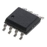
ICGOO电子元器件商城为您提供TC4429VOA由Microchip设计生产,在icgoo商城现货销售,并且可以通过原厂、代理商等渠道进行代购。 TC4429VOA价格参考¥10.85-¥14.29。MicrochipTC4429VOA封装/规格:PMIC - 栅极驱动器, Low-Side Gate Driver IC Inverting 8-SOIC。您可以下载TC4429VOA参考资料、Datasheet数据手册功能说明书,资料中有TC4429VOA 详细功能的应用电路图电压和使用方法及教程。
Microchip Technology的TC4429VOA是一款PMIC(电源管理集成电路)中的栅极驱动器,其应用场景主要集中在需要高效、快速开关的功率电子系统中。以下是该型号的具体应用场景:

1. 电机驱动:
   TC4429VOA适用于小型直流电机或步进电机的驱动电路,能够为MOSFET或IGBT提供足够的驱动电流以实现高效的开关控制。它支持高速切换,适合用于风扇、泵、家用电器等设备中的电机控制。

2. 电源转换:
   在DC-DC转换器或开关电源(SMPS)中,TC4429VOA可以驱动功率MOSFET或IGBT,确保高效的电压转换。其高输出电流能力(峰值可达1.5A)使其特别适合低功耗和中等功率的电源设计。

3. LED驱动:
   该器件可用于驱动大功率LED的应用中,例如汽车照明、工业照明或背光驱动。通过控制开关管的状态,它可以调节LED的亮度和电流。

4. 通信与网络设备:
   在路由器、交换机或其他通信设备中,TC4429VOA可用于驱动信号隔离器、继电器或功率级组件,确保信号的快速传输和稳定工作。

5. 消费类电子产品:
   包括便携式设备、音频放大器、游戏控制器等,这些设备通常需要高效的功率管理来延长电池寿命并优化性能。

6. 工业自动化:
   在PLC(可编程逻辑控制器)、传感器接口或工业机器人中,TC4429VOA可用于驱动负载或执行机构,确保快速响应和高可靠性。

7. 汽车电子:
   虽然TC4429VOA并非专为汽车环境设计,但在非关键任务的汽车应用中(如车窗升降器、座椅调节等),它也可以作为栅极驱动器使用。

总结来说,TC4429VOA凭借其高驱动能力、快速开关特性和宽泛的工作电压范围(4.5V至18V),成为许多功率电子系统的理想选择,尤其是在需要精确控制和高效能量转换的场景中。
| 参数 | 数值 |
| 产品目录 | 集成电路 (IC)半导体 |
| 描述 | IC MOSFET DRIVER 6A HS 8SOIC门驱动器 6A Sngl |
| 产品分类 | PMIC - MOSFET,电桥驱动器 - 外部开关集成电路 - IC |
| 品牌 | Microchip Technology |
| 产品手册 | |
| 产品图片 |
|
| rohs | 符合RoHS无铅 / 符合限制有害物质指令(RoHS)规范要求 |
| 产品系列 | 电源管理 IC,门驱动器,Microchip Technology TC4429VOA- |
| 数据手册 | http://www.microchip.com/mymicrochip/filehandler.aspx?ddocname=en011755 |
| 产品型号 | TC4429VOA |
| PCN组件/产地 | http://www.microchip.com/mymicrochip/NotificationDetails.aspx?id=5774&print=view |
| PCN设计/规格 | http://www.microchip.com/mymicrochip/NotificationDetails.aspx?id=5704&print=view |
| 上升时间 | 35 ns |
| 下降时间 | 35 ns |
| 产品 | MOSFET Gate Drivers |
| 产品种类 | 门驱动器 |
| 供应商器件封装 | 8-SOIC N |
| 包装 | 管件 |
| 商标 | Microchip Technology |
| 安装类型 | 表面贴装 |
| 安装风格 | SMD/SMT |
| 封装 | Tube |
| 封装/外壳 | 8-SOIC(0.154",3.90mm 宽) |
| 封装/箱体 | SOIC-8 |
| 工作温度 | -40°C ~ 125°C |
| 工厂包装数量 | 100 |
| 延迟时间 | 55ns |
| 最大功率耗散 | 470 mW |
| 最大工作温度 | + 125 C |
| 最小工作温度 | - 40 C |
| 标准包装 | 100 |
| 激励器数量 | 1 Driver |
| 电压-电源 | 4.5 V ~ 18 V |
| 电流-峰值 | 6A |
| 电源电压-最大 | 18 V |
| 电源电压-最小 | 4.5 V |
| 电源电流 | 3 mA |
| 类型 | Low Side |
| 输入类型 | 反相 |
| 输出数 | 1 |
| 输出端数量 | 1 |
| 配置 | Inverting |
| 配置数 | 1 |
| 高压侧电压-最大值(自举) | - |


- 商务部:美国ITC正式对集成电路等产品启动337调查
- 曝三星4nm工艺存在良率问题 高通将骁龙8 Gen1或转产台积电
- 太阳诱电将投资9.5亿元在常州建新厂生产MLCC 预计2023年完工
- 英特尔发布欧洲新工厂建设计划 深化IDM 2.0 战略
- 台积电先进制程称霸业界 有大客户加持明年业绩稳了
- 达到5530亿美元!SIA预计今年全球半导体销售额将创下新高
- 英特尔拟将自动驾驶子公司Mobileye上市 估值或超500亿美元
- 三星加码芯片和SET,合并消费电子和移动部门,撤换高东真等 CEO
- 三星电子宣布重大人事变动 还合并消费电子和移动部门
- 海关总署:前11个月进口集成电路产品价值2.52万亿元 增长14.8%


PDF Datasheet 数据手册内容提取
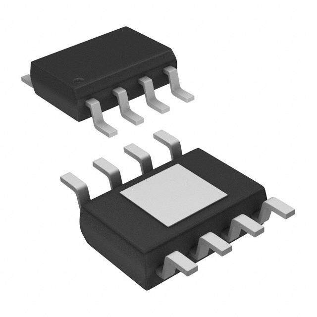
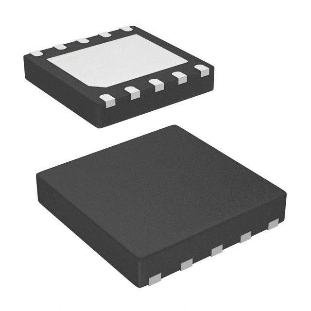
TC4420/TC4429 6A High-Speed MOSFET Drivers Features General Description • Latch-Up Protected: Will Withstand >1.5A The TC4420/TC4429 are 6A (peak), single-output Reverse Output Current MOSFET drivers. The TC4429 is an inverting driver • Logic Input Will Withstand Negative Swing Up To (pin-compatible with the TC429), while the TC4420 is a 5V non-inverting driver. These drivers are fabricated in CMOS for lower power and more efficient operation • ESD Protected: 4kV versus bipolar drivers. • Matched Rise and Fall Times: Both devices have TTL/CMOS compatible inputs that - 25ns (2500pF load) can be driven as high as V + 0.3V or as low as –5V • High Peak Output Current: 6A DD without upset or damage to the device. This eliminates • Wide Input Supply Voltage Operating Range: the need for external level-shifting circuitry and its - 4.5V to 18V associated cost and size. The output swing is rail-to-rail, • High Capacitive Load Drive Capability: 10,000pF ensuring better drive voltage margin, especially during • Short Delay Time: 55ns (typ.) power-up/power-down sequencing. Propagational delay time is only 55ns (typ.) and the output rise and fall • CMOS/TTL Compatible Input times are only 25ns (typ.) into 2500pF across the • Low Supply Current With Logic ‘1’ Input: usable power supply range. - 450µA (typ.) Unlike other drivers, the TC4420/TC4429 are virtually • Low Output Impedance: 2.5 latch-up proof. They replace three or more discrete • Output Voltage Swing to Within 25mV of Ground components, saving PCB area, parts and improving or VDD overall system reliability. • Space-Saving 8-Pin SOIC and 8-Pin 6x5 DFN Packages Applications • Switch-Mode Power Supplies • Motor Controls • Pulse Transformer Driver • Class D Switching Amplifiers Package Types(1) 8-Pin CERDIP/ TC4420 TC4429 8-Pin DFN(2) TC4420 TC4429 5-Pin TO-220 PDIP/SOIC Tab is VDD 1 8 VDD VDD VDD 1 8 VDD VDD Common INPUT 2 TC4420 7 OUTPUT OUTPUT INPUT 2 TC4420 7 OUTPUT OUTPUT to VDD NC 3 TC4429 6 OUTPUT OUTPUT NC 3 TC4429 6 OUTPUT OUTPUT TC4420 TC4429 GND 4 5 GND GND GND 4 5 GND GND Note 1: Duplicate pins must both be connected for proper operation. NPUTGNDVDDGNDTPUT I U 2: Exposed pad of the DFN package is electrically isolated. O 2002-2012 Microchip Technology Inc. DS21419D-page 1
TC4420/TC4429 Functional Block Diagram V DD TC4429 Inverting 500µA 300mV Output TC4420 Input Non-Inverting 4.7V GND Effective Input C = 38pF DS21419D-page 2 2002-2012 Microchip Technology Inc.
TC4420/TC4429 1.0 ELECTRICAL † Stresses above those listed under “Absolute Maximum Ratings” may cause permanent damage to the device. These CHARACTERISTICS are stress ratings only and functional operation of the device at these or any other conditions above those indicated in the Absolute Maximum Ratings† operation sections of the specifications is not implied. Exposure to Absolute Maximum Rating conditions for Supply Voltage.....................................................+20V extended periods may affect device reliability. Input Voltage..................................– 5V to V + 0.3V DD Input Current (V > V )...................................50mA IN DD Power Dissipation (T 70°C) A 5-Pin TO-220....................................................1.6W CERDIP.......................................................800mW DFN...............................................................Note2 PDIP............................................................730mW SOIC............................................................470mW Package Power Dissipation (T 25°C) A 5-Pin TO-220 (With Heatsink)........................12.5W Thermal Impedances (To Case) 5-Pin TO-220 R ......................................10°C/W J-C DC CHARACTERISTICS Electrical Specifications: Unless otherwise noted, T = +25°C with 4.5V V 18V. A DD Parameters Sym Min Typ Max Units Conditions Input Logic ‘1’, High Input VIH 2.4 1.8 — V Voltage Logic ‘0’, Low Input Voltage VIL — 1.3 0.8 V Input Voltage Range V –5 — V +0.3 V IN DD Input Current I –10 — +10 µA 0VV V IN IN DD Output High Output Voltage V V – 0.025 — — V DC TEST OH DD Low Output Voltage V — — 0.025 V DC TEST OL Output Resistance, High R — 2.1 2.8 I = 10mA, V = 18V OH OUT DD Output Resistance, Low R — 1.5 2.5 I = 10mA, V = 18V OL OUT DD Peak Output Current I — 6.0 — A V = 18V PK DD Latch-Up Protection I — > 1.5 — A Duty cycle2%, t 300µsec REV Withstand Reverse Current Switching Time (Note1) Rise Time t — 25 35 ns Figure4-1, C = 2,500pF R L Fall Time t — 25 35 ns Figure4-1, C = 2,500pF F L Delay Time t — 55 75 ns Figure4-1 D1 Delay Time t — 55 75 ns Figure4-1 D2 Power Supply Power Supply Current I — 0.45 1.5 mA V = 3V S IN — 55 150 µA V = 0V IN Operating Input Voltage V 4.5 — 18 V DD Note 1: Switching times ensured by design. 2: Package power dissipation is dependent on the copper pad area on the PCB. 2002-2012 Microchip Technology Inc. DS21419D-page 3
TC4420/TC4429 DC CHARACTERISTICS (OVER OPERATING TEMPERATURE RANGE) Electrical Specifications: Unless otherwise noted, over operating temperature range with 4.5V V 18V. DD Parameters Sym Min Typ Max Units Conditions Input Logic ‘1’, High Input VIH 2.4 — — V Voltage Logic ‘0’, Low Input Voltage VIL — — 0.8 V Input Voltage Range V –5 — V + 0.3 V IN DD Input Current I –10 — +10 µA 0VV V IN IN DD Output High Output Voltage V V – 0.025 — — V DC TEST OH DD Low Output Voltage V — — 0.025 V DC TEST OL Output Resistance, High R — 3 5 I = 10mA, V = 18V OH OUT DD Output Resistance, Low R — 2.3 5 I = 10mA, V = 18V OL OUT DD Switching Time (Note1) Rise Time t — 32 60 ns Figure4-1, C = 2,500pF R L Fall Time t — 34 60 ns Figure4-1, C = 2,500pF F L Delay Time t — 50 100 ns Figure4-1 D1 Delay Time t — 65 100 ns Figure4-1 D2 Power Supply Power Supply Current I — 0.45 3 mA V = 3V S IN — 60 400 µA V = 0V IN Operating Input Voltage V 4.5 — 18 V DD Note 1: Switching times ensured by design. TEMPERATURE CHARACTERISTICS Electrical Specifications: Unless otherwise noted, all parameters apply with 4.5V V 18V. DD Parameters Sym Min Typ Max Units Conditions Temperature Ranges Specified Temperature Range (C) T 0 — +70 °C A Specified Temperature Range (I) T –25 — +85 °C A Specified Temperature Range (E) T –40 — +85 °C A Specified Temperature Range (V) T –40 — +125 °C A Maximum Junction Temperature T — — +150 °C J Storage Temperature Range T –65 — +150 °C A Package Thermal Resistances Thermal Resistance, 5L-TO-220 — 71 — °C/W JA Thermal Resistance, 8L-CERDIP — 150 — °C/W JA Thermal Resistance, 8L-6x5 DFN — 33.2 — °C/W Typical four-layer board JA with vias to ground plane. Thermal Resistance, 8L-PDIP — 125 — °C/W JA Thermal Resistance, 8L-SOIC — 155 — °C/W JA DS21419D-page 4 2002-2012 Microchip Technology Inc.
TC4420/TC4429 2.0 TYPICAL PERFORMANCE CURVES Note: The graphs and tables provided following this note are a statistical summary based on a limited number of samples and are provided for informational purposes only. The performance characteristics listed herein are not tested or guaranteed. In some graphs or tables, the data presented may be outside the specified operating range (e.g., outside specified power supply range) and therefore outside the warranted range. Note: Unless otherwise indicated, T = +25°C with 4.5V V 18V. A DD 120 100 100 C L = 10,000 pF 80 80 Time (nsec) 60 C L = 4700 pF me (nsec) 6400 C CL =L =1 04,700000 ppFF 40 Ti C L = 2200 pF C L = 2200 pF 20 20 0 0 5 7 9 11 13 15 5 7 9 11 13 15 Supply Voltage (V) Supply Voltage (V) FIGURE 2-1: Rise Time vs. Supply FIGURE 2-4: Fall Time vs. Supply Voltage. Voltage. 100 100 80 80 60 60 Time (nsec) 40 VVD D D D = = 1 52VV VD D = 18V Time (nsec)40 VVDD D D == 152VV VD D = 18V 20 20 10 10 1000 10,000 1000 10,000 Capcitive Load (pF) Capacitive Load (pF) FIGURE 2-2: Rise Time vs. Capacitive FIGURE 2-5: Fall Time vs. Capacitive Load. Load. 50 84 C L = 2200 pF VD D = 15V VD D = 18V 70 40 Delay Time (nsec)3200 tD2 tD1 pply Current (mA)542628 500 kHz u 10 S 200 kHz 14 20 kHz 0 0 –60 –20 20 60 100 140 0 100 1000 10,000 TA (°C) Capacitive Load (pF) FIGURE 2-3: Propagation Delay Time vs. FIGURE 2-6: Supply Current vs. Temperature. Capacitive Load. 2002-2012 Microchip Technology Inc. DS21419D-page 5
TC4420/TC4429 Note: Unless otherwise indicated, T = +25°C with 4.5V V 18V. A DD 50 5 C L = 2200 pF VD D = 18V 40 100 mA 4 Time (nsec)3200 tFALL tRISE ΩR ( )OUT 10 mA 50 mA 3 10 0 2 –60 –20 20 60 100 140 5 7 9 11 13 15 TA (°C) Supply Voltage (V) FIGURE 2-7: Rise and Fall Times vs. FIGURE 2-10: High-State Output Temperature. Resistance vs Supply Voltage. 65 200 Load = 2200 pF 60 160 Delay Time (nsec)554505 ttDD21 Delay Time (nsec)12800 InputI n2p.4uIVnt p3uVt 5V 40 40 Input 8V and 10V 35 0 4 6 8 10 12 14 16 18 5 6 7 8 9 10 11 12 13 14 15 Supply Voltage (V) V D D (V) FIGURE 2-8: Propagation Delay Time vs. FIGURE 2-11: Effect of Input Amplitude on Supply Voltage. Propagation Delay. 1000 2.5 C L = 2200 pF 18V ply Current (mA) 100 150VV ΩR ( )OUT 2 100 mA50 mA up 10 1.5 S 10 mA 0 1 0 100 1000 10,000 5 7 9 11 13 15 Frequency (kHz) Supply Voltage (V) FIGURE 2-9: Supply Current vs. FIGURE 2-12: Low-State Output Frequency. Resistance vs. Supply Voltage. DS21419D-page 6 2002-2012 Microchip Technology Inc.
TC4420/TC4429 Note: Unless otherwise indicated, T = +25°C with 4.5V V 18V. A DD 4 -80 1 3 S) x A(cid:129) ea ( 2 Ar er ov oss 1 Cr 0 5 6 7 8 9 10 11 12 13 14 15 Supply Voltage (V) The values on this graph represent the loss seen by the driver during one complete cycle. For a single transition, divide the value by 2. FIGURE 2-13: Crossover Energy. 2002-2012 Microchip Technology Inc. DS21419D-page 7
TC4420/TC4429 3.0 PIN DESCRIPTIONS The descriptions of the pins are listed in Table3-1. TABLE 3-1: PIN FUNCTION TABLE Pin No. Pin No. Pin No. 8-Pin CERDIP/ Symbol Description 8-Pin DFN 5-Pin TO-220 PDIP/SOIC 1 1 — V Supply input, 4.5V to 18V DD 2 2 1 INPUT Control input, TTL/CMOS compatible input 3 3 — NC No Connection 4 4 2 GND Ground 5 5 4 GND Ground 6 6 5 OUTPUT CMOS push-pull output 7 7 — OUTPUT CMOS push-pull output 8 8 3 V Supply input, 4.5V to 18V DD — PAD — NC Exposed Metal Pad — — TAB V Metal Tab is at the V Potential DD DD 3.1 Supply Input (V ) 3.3 CMOS Push-Pull Output DD The V input is the bias supply for the MOSFET driver The MOSFET driver output is a low-impedance, DD and is rated for 4.5V to 18V with respect to the ground CMOS, push-pull style output capable of driving a pins. The V input should be bypassed to ground with capacitive load with 6.0A peak currents. The MOSFET DD a local ceramic capacitor. The value of the capacitor driver output is capable of withstanding 1.5A peak should be chosen based on the capacitive load that is reverse currents of either polarity. being driven. A minimum value of 1.0µF is suggested. 3.4 Ground 3.2 Control Input The ground pins are the return path for the bias current The MOSFET driver input is a high-impedance, and the high peak currents that discharge the load TTL/CMOS compatible input. The input circuitry of the capacitor. The ground pins should be tied into a ground TC4420/TC4429 MOSFET driver also has a “speed- plane or have very short traces to the bias supply up” capacitor. This helps to decrease the propagation source return. delay times of the driver. Because of this, input signals with slow rising or falling edges should not be used, as 3.5 Exposed Metal Pad this can result in double-pulsing of the MOSFET driver output. The exposed metal pad of the 6x5 DFN package is not internally connected to any potential. Therefore, this pad can be connected to a ground plane or other copper plane on a printed circuit board (PCB) to aid in heat removal from the package. DS21419D-page 8 2002-2012 Microchip Technology Inc.
TC4420/TC4429 4.0 APPLICATIONS INFORMATION +5V 90% Input VDD = 18V 0V 10% tD1 tD2 t t F R 4.7µF +18V 90% 90% 1 8 Output 10% 10% 0.1µF 0.1µF 0V Inverting Driver Input 2 6 Output TC4429 7 +5V C = 2,500pF 90% L Input 4 5 10% 0V +18V 90% 90% tD1 tD2 Output tR tF Input: 100kHz, square wave, 0V 10% 10% t = t 10ns RISE FALL Non-Inverting Driver TC4420 Note: Pinout shown is for the PDIP, SOIC, DFN and CERDIP packages. FIGURE 4-1: Switching Time Test Circuits. 2002-2012 Microchip Technology Inc. DS21419D-page 9
TC4420/TC4429 5.0 PACKAGING INFORMATION 5.1 Package Marking Information 5-Lead TO-220 Example: XXXXXXXXX TC4420CAT XXXXXXXXX 0419256 YYWWNNN 8-Lead CERDIP (300 mil) Example: XXXXXXXX TC4420 XXXXXNNN MJA256 YYWW 0419 8-Lead DFN Example: XXXXXXX TC4420 XXXXXXX EMF XXYYWW 0419 NNN 256 Legend: XX...X Customer-specific information Y Year code (last digit of calendar year) YY Year code (last 2 digits of calendar year) WW Week code (week of January 1 is week ‘01’) NNN Alphanumeric traceability code e3 Pb-free JEDEC designator for Matte Tin (Sn) * This package is Pb-free. The Pb-free JEDEC designator ( e 3 ) can be found on the outer packaging for this package. Note: In the event the full Microchip part number cannot be marked on one line, it will be carried over to the next line, thus limiting the number of available characters for customer-specific information. DS21419D-page 10 2002-2012 Microchip Technology Inc.
TC4420/TC4429 Package Marking Information (Continued) 8-Lead PDIP (300 mil) Example: XXXXXXXX TC4420 XXXXXNNN CPA256 YYWW 0419 8-Lead SOIC (150 mil) Example: XXXXXXXX TC4420 XXXXYYWW EOA0419 NNN 256 2002-2012 Microchip Technology Inc. DS21419D-page 11
TC4420/TC4429 5-Lead Plastic Transistor Outline (AT) (TO-220) Note: For the most current package drawings, please see the Microchip Packaging Specification located at http://www.microchip.com/packaging L H1 Q b e3 e1 E e EJECTOR PIN ØP a(5X) C1 A J1 F D Units INCHES* MILLIMETERS Dimension Limits MIN MAX MIN MAX Lead Pitch e .060 .072 1.52 1.83 Overall Lead Centers e1 .263 .273 6.68 6.93 Space Between Leads e3 .030 .040 0.76 1.02 Overall Height A .160 .190 4.06 4.83 Overall Width E .385 .415 9.78 10.54 Overall Length D .560 .590 14.22 14.99 Flag Length H1 .234 .258 5.94 6.55 Flag Thickness F .045 .055 1.14 1.40 Through Hole Center Q .103 .113 2.62 2.87 Through Hole Diameter P .146 .156 3.71 3.96 Lead Length L .540 .560 13.72 14.22 Base to Bottom of Lead J1 .090 .115 2.29 2.92 Lead Thickness C1 .014 .022 0.36 0.56 Lead Width b .025 .040 0.64 1.02 Mold Draft Angle a 3° 7° 3° 7° *Controlling Parameter Notes: Dimensions D and E1 do not include mold flash or protrusions. Mold flash or protrusions shall not exceed .010" (0.254mm) per side. JEDEC equivalent: TO-220 Drawing No. C04-036 DS21419D-page 12 2002-2012 Microchip Technology Inc.
TC4420/TC4429 8-Lead Ceramic Dual In-line – 300 mil (JA) (CERDIP) Note: For the most current package drawings, please see the Microchip Packaging Specification located at http://www.microchip.com/packaging E1 2 n 1 D E A2 A c L eB B1 B A1 p Units INCHES* MILLIMETERS Dimension Limits MIN NOM MAX MIN NOM MAX Number of Pins n 8 8 Pitch p .100 2.54 Top to Seating Plane A .160 .180 .200 4.06 4.57 5.08 Standoff § A1 .020 .030 .040 0.51 0.77 1.02 Shoulder to Shoulder Width E .290 .305 .320 7.37 7.75 8.13 Ceramic Pkg. Width E1 .230 .265 .300 5.84 6.73 7.62 Overall Length D .370 .385 .400 9.40 9.78 10.16 Tip to Seating Plane L .125 .163 .200 3.18 4.13 5.08 Lead Thickness c .008 .012 .015 0.20 0.29 0.38 Upper Lead Width B1 .045 .055 .065 1.14 1.40 1.65 Lower Lead Width B .016 .018 .020 0.41 0.46 0.51 Overall Row Spacing eB .320 .360 .400 8.13 9.15 10.16 *Controlling Parameter JEDEC Equivalent: MS-030 Drawing No. C04-010 2002-2012 Microchip Technology Inc. DS21419D-page 13
TC4420/TC4429 8-Lead Plastic Dual Flat No Lead Package (MF) 6x5 mm Body (DFN-S) – Saw Singulated Note: For the most current package drawings, please see the Microchip Packaging Specification located at http://www.microchip.com/packaging DS21419D-page 14 2002-2012 Microchip Technology Inc.
TC4420/TC4429 8-Lead Plastic Dual In-line (PA) – 300 mil (PDIP) Note: For the most current package drawings, please see the Microchip Packaging Specification located at http://www.microchip.com/packaging E1 D 2 n 1 E A A2 L c A1 B1 p eB B Units INCHES* MILLIMETERS Dimension Limits MIN NOM MAX MIN NOM MAX Number of Pins n 8 8 Pitch p .100 2.54 Top to Seating Plane A .140 .155 .170 3.56 3.94 4.32 Molded Package Thickness A2 .115 .130 .145 2.92 3.30 3.68 Base to Seating Plane A1 .015 0.38 Shoulder to Shoulder Width E .300 .313 .325 7.62 7.94 8.26 Molded Package Width E1 .240 .250 .260 6.10 6.35 6.60 Overall Length D .360 .373 .385 9.14 9.46 9.78 Tip to Seating Plane L .125 .130 .135 3.18 3.30 3.43 Lead Thickness c .008 .012 .015 0.20 0.29 0.38 Upper Lead Width B1 .045 .058 .070 1.14 1.46 1.78 Lower Lead Width B .014 .018 .022 0.36 0.46 0.56 Overall Row Spacing § eB .310 .370 .430 7.87 9.40 10.92 Mold Draft Angle Top 5 10 15 5 10 15 Mold Draft Angle Bottom 5 10 15 5 10 15 * Controlling Parameter § Significant Characteristic Notes: Dimensions D and E1 do not include mold flash or protrusions. Mold flash or protrusions shall not exceed .010” (0.254mm) per side. JEDEC Equivalent: MS-001 Drawing No. C04-018 2002-2012 Microchip Technology Inc. DS21419D-page 15
TC4420/TC4429 8-Lead Plastic Small Outline (OA) – Narrow, 150 mil (SOIC) Note: For the most current package drawings, please see the Microchip Packaging Specification located at http://www.microchip.com/packaging E E1 p D 2 B n 1 h 45 c A A2 L A1 Units INCHES* MILLIMETERS Dimension Limits MIN NOM MAX MIN NOM MAX Number of Pins n 8 8 Pitch p .050 1.27 Overall Height A .053 .061 .069 1.35 1.55 1.75 Molded Package Thickness A2 .052 .056 .061 1.32 1.42 1.55 Standoff § A1 .004 .007 .010 0.10 0.18 0.25 Overall Width E .228 .237 .244 5.79 6.02 6.20 Molded Package Width E1 .146 .154 .157 3.71 3.91 3.99 Overall Length D .189 .193 .197 4.80 4.90 5.00 Chamfer Distance h .010 .015 .020 0.25 0.38 0.51 Foot Length L .019 .025 .030 0.48 0.62 0.76 Foot Angle 0 4 8 0 4 8 Lead Thickness c .008 .009 .010 0.20 0.23 0.25 Lead Width B .013 .017 .020 0.33 0.42 0.51 Mold Draft Angle Top 0 12 15 0 12 15 Mold Draft Angle Bottom 0 12 15 0 12 15 * Controlling Parameter § Significant Characteristic Notes: Dimensions D and E1 do not include mold flash or protrusions. Mold flash or protrusions shall not exceed .010” (0.254mm) per side. JEDEC Equivalent: MS-012 Drawing No. C04-057 DS21419D-page 16 2002-2012 Microchip Technology Inc.
TC4420/TC4429 6.0 REVISION HISTORY Revision D (December 2012) Added a note to each package outline drawing. 2002-2012 Microchip Technology Inc. DS21419D-page 17
TC4420/TC4429 NOTES: DS21419D-page 18 2002-2012 Microchip Technology Inc.
TC4420/TC4429 PRODUCT IDENTIFICATION SYSTEM To order or obtain information, e.g., on pricing or delivery, refer to the factory or the listed sales office. PART NO. X XX XXX X Examples: a) TC4420CAT: 6A High-Speed MOSFET Device Temperature Package Tape and PB Free Driver, Non-inverting, Range Reel TO-220 package, 0°C to +70°C. b) TC4420EOA: 6A High-Speed MOSFET Device: TC4420: 6A High-Speed MOSFET Driver, Non-Inverting TC4429: 6A High-Speed MOSFET Driver, Inverting Driver, Non-inverting, SOIC package, -40°C to +85°C. Temperature Range: C = 0°C to +70°C (PDIP, SOIC, and TO-220 Only) c) TC4420VMF: 6A High-Speed MOSFET I = -25°C to +85°C (CERDIP Only) E = -40°C to +85°C Driver, Non-inverting, V = -40°C to +125°C DFN package, -40°C to +125°C. Package: AT = TO-220, 5-lead (C-Temp Only) a) TC4429CAT: 6A High-Speed MOSFET JA = Ceramic Dual In-line (300 mil Body), 8-lead Driver, Inverting, (I-Temp Only) TO-220 package, MF = Dual, Flat, No-Lead (6X5 mm Body), 8-lead 0°C to +70°C MF713 = Dual, Flat, No-Lead (6X5 mm Body), 8-lead (Tape and Reel) b) TC4429EPA: 6A High-Speed MOSFET PA = Plastic DIP (300 mil Body), 8-lead Driver, Inverting, OA = Plastic SOIC, (150 mil Body), 8-lead PDIP package, OA713 = Plastic SOIC, (150 mil Body), 8-lead -40°C to +85°C (Tape and Reel) c) TC4429VMF: 6A High-Speed MOSFET PB Free G = Lead-Free device* = Blank Driver, Inverting, DFN package, * Available on selected packages. Contact your local sales -40°C to +125°C representative for availability Sales and Support Data Sheets Products supported by a preliminary Data Sheet may have an errata sheet describing minor operational differences and recommended workarounds. To determine if an errata sheet exists for a particular device, please contact one of the following: 1. Your local Microchip sales office 2. The Microchip Worldwide Site (www.microchip.com) Please specify which device, revision of silicon and Data Sheet (include Literature #) you are using. Customer Notification System Register on our web site (www.microchip.com/cn) to receive the most current information on our products. 2002-2012 Microchip Technology Inc. DS21419D-page 19
TC4420/TC4429 NOTES: DS21419D-page 20 2002-2012 Microchip Technology Inc.
Note the following details of the code protection feature on Microchip devices: • Microchip products meet the specification contained in their particular Microchip Data Sheet. • Microchip believes that its family of products is one of the most secure families of its kind on the market today, when used in the intended manner and under normal conditions. • There are dishonest and possibly illegal methods used to breach the code protection feature. All of these methods, to our knowledge, require using the Microchip products in a manner outside the operating specifications contained in Microchip’s Data Sheets. Most likely, the person doing so is engaged in theft of intellectual property. • Microchip is willing to work with the customer who is concerned about the integrity of their code. • Neither Microchip nor any other semiconductor manufacturer can guarantee the security of their code. Code protection does not mean that we are guaranteeing the product as “unbreakable.” Code protection is constantly evolving. We at Microchip are committed to continuously improving the code protection features of our products. Attempts to break Microchip’s code protection feature may be a violation of the Digital Millennium Copyright Act. If such acts allow unauthorized access to your software or other copyrighted work, you may have a right to sue for relief under that Act. Information contained in this publication regarding device Trademarks applications and the like is provided only for your convenience The Microchip name and logo, the Microchip logo, dsPIC, and may be superseded by updates. It is your responsibility to FlashFlex, KEELOQ, KEELOQ logo, MPLAB, PIC, PICmicro, ensure that your application meets with your specifications. PICSTART, PIC32 logo, rfPIC, SST, SST Logo, SuperFlash MICROCHIP MAKES NO REPRESENTATIONS OR and UNI/O are registered trademarks of Microchip Technology WARRANTIES OF ANY KIND WHETHER EXPRESS OR Incorporated in the U.S.A. and other countries. IMPLIED, WRITTEN OR ORAL, STATUTORY OR OTHERWISE, RELATED TO THE INFORMATION, FilterLab, Hampshire, HI-TECH C, Linear Active Thermistor, INCLUDING BUT NOT LIMITED TO ITS CONDITION, MTP, SEEVAL and The Embedded Control Solutions QUALITY, PERFORMANCE, MERCHANTABILITY OR Company are registered trademarks of Microchip Technology FITNESS FOR PURPOSE. Microchip disclaims all liability Incorporated in the U.S.A. arising from this information and its use. Use of Microchip Silicon Storage Technology is a registered trademark of devices in life support and/or safety applications is entirely at Microchip Technology Inc. in other countries. the buyer’s risk, and the buyer agrees to defend, indemnify and Analog-for-the-Digital Age, Application Maestro, BodyCom, hold harmless Microchip from any and all damages, claims, chipKIT, chipKIT logo, CodeGuard, dsPICDEM, suits, or expenses resulting from such use. No licenses are dsPICDEM.net, dsPICworks, dsSPEAK, ECAN, conveyed, implicitly or otherwise, under any Microchip ECONOMONITOR, FanSense, HI-TIDE, In-Circuit Serial intellectual property rights. Programming, ICSP, Mindi, MiWi, MPASM, MPF, MPLAB Certified logo, MPLIB, MPLINK, mTouch, Omniscient Code Generation, PICC, PICC-18, PICDEM, PICDEM.net, PICkit, PICtail, REAL ICE, rfLAB, Select Mode, SQI, Serial Quad I/O, Total Endurance, TSHARC, UniWinDriver, WiperLock, ZENA and Z-Scale are trademarks of Microchip Technology Incorporated in the U.S.A. and other countries. SQTP is a service mark of Microchip Technology Incorporated in the U.S.A. GestIC and ULPP are registered trademarks of Microchip Technology Germany II GmbH & Co. & KG, a subsidiary of Microchip Technology Inc., in other countries. All other trademarks mentioned herein are property of their respective companies. © 2002-2012, Microchip Technology Incorporated, Printed in the U.S.A., All Rights Reserved. Printed on recycled paper. ISBN: 9781620767948 QUALITY MANAGEMENT SYSTEM Microchip received ISO/TS-16949:2009 certification for its worldwide headquarters, design and wafer fabrication facilities in Chandler and CERTIFIED BY DNV Tempe, Arizona; Gresham, Oregon and design centers in California and India. The Company’s quality system processes and procedures == ISO/TS 16949 == are for its PIC® MCUs and dsPIC® DSCs, KEELOQ® code hopping devices, Serial EEPROMs, microperipherals, nonvolatile memory and analog products. In addition, Microchip’s quality system for the design and manufacture of development systems is ISO 9001:2000 certified. 2002-2012 Microchip Technology Inc. DS21419D-page 21
Worldwide Sales and Service AMERICAS ASIA/PACIFIC ASIA/PACIFIC EUROPE Corporate Office Asia Pacific Office India - Bangalore Austria - Wels 2355 West Chandler Blvd. Suites 3707-14, 37th Floor Tel: 91-80-3090-4444 Tel: 43-7242-2244-39 Chandler, AZ 85224-6199 Tower 6, The Gateway Fax: 91-80-3090-4123 Fax: 43-7242-2244-393 Tel: 480-792-7200 Harbour City, Kowloon India - New Delhi Denmark - Copenhagen Fax: 480-792-7277 Hong Kong Tel: 91-11-4160-8631 Tel: 45-4450-2828 Technical Support: Tel: 852-2401-1200 Fax: 91-11-4160-8632 Fax: 45-4485-2829 http://www.microchip.com/ support Fax: 852-2401-3431 India - Pune France - Paris Web Address: Australia - Sydney Tel: 91-20-2566-1512 Tel: 33-1-69-53-63-20 www.microchip.com Tel: 61-2-9868-6733 Fax: 91-20-2566-1513 Fax: 33-1-69-30-90-79 Atlanta Fax: 61-2-9868-6755 Japan - Osaka Germany - Munich Duluth, GA China - Beijing Tel: 81-66-152-7160 Tel: 49-89-627-144-0 Tel: 86-10-8569-7000 Fax: 49-89-627-144-44 Tel: 678-957-9614 Fax: 81-66-152-9310 Fax: 678-957-1455 Fax: 86-10-8528-2104 Japan - Yokohama Italy - Milan China - Chengdu Tel: 39-0331-742611 Boston Tel: 81-45-471- 6166 Tel: 86-28-8665-5511 Fax: 39-0331-466781 Westborough, MA Fax: 81-45-471-6122 Tel: 774-760-0087 Fax: 86-28-8665-7889 Korea - Daegu Netherlands - Drunen Fax: 774-760-0088 China - Chongqing Tel: 82-53-744-4301 Tel: 31-416-690399 Chicago Tel: 86-23-8980-9588 Fax: 82-53-744-4302 Fax: 31-416-690340 Itasca, IL Fax: 86-23-8980-9500 Korea - Seoul Spain - Madrid Tel: 630-285-0071 China - Hangzhou Tel: 82-2-554-7200 Tel: 34-91-708-08-90 Fax: 630-285-0075 Tel: 86-571-2819-3187 Fax: 82-2-558-5932 or Fax: 34-91-708-08-91 Cleveland Fax: 86-571-2819-3189 82-2-558-5934 UK - Wokingham Independence, OH China - Hong Kong SAR Malaysia - Kuala Lumpur Tel: 44-118-921-5869 Tel: 216-447-0464 Tel: 852-2943-5100 Tel: 60-3-6201-9857 Fax: 44-118-921-5820 Fax: 216-447-0643 Fax: 852-2401-3431 Fax: 60-3-6201-9859 Dallas China - Nanjing Malaysia - Penang Addison, TX Tel: 86-25-8473-2460 Tel: 60-4-227-8870 Tel: 972-818-7423 Fax: 86-25-8473-2470 Fax: 60-4-227-4068 Fax: 972-818-2924 China - Qingdao Philippines - Manila Detroit Tel: 86-532-8502-7355 Tel: 63-2-634-9065 Farmington Hills, MI Fax: 86-532-8502-7205 Fax: 63-2-634-9069 Tel: 248-538-2250 Fax: 248-538-2260 China - Shanghai Singapore Tel: 86-21-5407-5533 Tel: 65-6334-8870 Indianapolis Fax: 86-21-5407-5066 Fax: 65-6334-8850 Noblesville, IN Tel: 317-773-8323 China - Shenyang Taiwan - Hsin Chu Fax: 317-773-5453 Tel: 86-24-2334-2829 Tel: 886-3-5778-366 Fax: 86-24-2334-2393 Fax: 886-3-5770-955 Los Angeles Mission Viejo, CA China - Shenzhen Taiwan - Kaohsiung Tel: 949-462-9523 Tel: 86-755-8864-2200 Tel: 886-7-213-7828 Fax: 949-462-9608 Fax: 86-755-8203-1760 Fax: 886-7-330-9305 Santa Clara China - Wuhan Taiwan - Taipei Santa Clara, CA Tel: 86-27-5980-5300 Tel: 886-2-2508-8600 Tel: 408-961-6444 Fax: 86-27-5980-5118 Fax: 886-2-2508-0102 Fax: 408-961-6445 China - Xian Thailand - Bangkok Toronto Tel: 86-29-8833-7252 Tel: 66-2-694-1351 Mississauga, Ontario, Fax: 86-29-8833-7256 Fax: 66-2-694-1350 Canada China - Xiamen Tel: 905-673-0699 Tel: 86-592-2388138 Fax: 905-673-6509 Fax: 86-592-2388130 China - Zhuhai Tel: 86-756-3210040 11/27/12 Fax: 86-756-3210049 DS21419D-page 22 2002-2012 Microchip Technology Inc.