ICGOO在线商城 > 隔离器 > 隔离器 - 栅极驱动器 > Si8232BB-B-IS

 Datasheet下载
- 型号: Si8232BB-B-IS
- 制造商: Silicon Laboratories
- 库位|库存: xxxx|xxxx
- 要求:
| 数量阶梯 | 香港交货 | 国内含税 |
| +xxxx | $xxxx | ¥xxxx |
查看当月历史价格
查看今年历史价格
Si8232BB-B-IS产品简介:
ICGOO电子元器件商城为您提供Si8232BB-B-IS由Silicon Laboratories设计生产,在icgoo商城现货销售,并且可以通过原厂、代理商等渠道进行代购。 Si8232BB-B-IS价格参考。Silicon LaboratoriesSi8232BB-B-IS封装/规格:隔离器 - 栅极驱动器, 500mA Gate Driver 容性耦合 2500Vrms 2 Channel 16-SOIC。您可以下载Si8232BB-B-IS参考资料、Datasheet数据手册功能说明书,资料中有Si8232BB-B-IS 详细功能的应用电路图电压和使用方法及教程。
Silicon Labs 的 SI8232BB-B-IS 是一款高性能的数字隔离式栅极驱动器,广泛应用于需要高效、可靠驱动功率开关器件(如MOSFET或IGBT)的场合。其主要应用场景包括:

1. 电机控制:用于工业自动化设备中的电机驱动系统,提供安全隔离和高效驱动能力,适用于变频器和伺服驱动器等。

2. 电源转换系统:如DC-DC转换器、AC-DC电源模块,SI8232BB-B-IS可有效驱动高频开关器件,提升转换效率和系统稳定性。

3. 新能源领域:在太阳能逆变器、储能系统和电动汽车充电设备中,用于隔离控制电路与高压功率电路,确保系统安全与高效运行。

4. 工业逆变器与UPS系统:在不间断电源(UPS)和工业逆变器中,作为功率开关的驱动核心,提供高抗噪能力和电气隔离,增强系统可靠性。

5. 家电与白色家电:如变频空调、洗衣机等,用于驱动内部功率模块,实现节能与小型化设计。

该器件具备高隔离电压、低传播延迟和宽工作温度范围等优点,适合在复杂电磁环境和严苛工况下稳定运行。
| 参数 | 数值 |
| 产品目录 | |
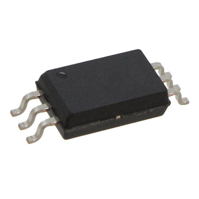
| 描述 | DGTL ISO 2.5KV GATE DRVR 16SOIC门驱动器 0.5A Dual Low Side ISOdriver |
| 产品分类 | |
| 品牌 | Silicon Laboratories IncSilicon Labs |
| 产品手册 | |
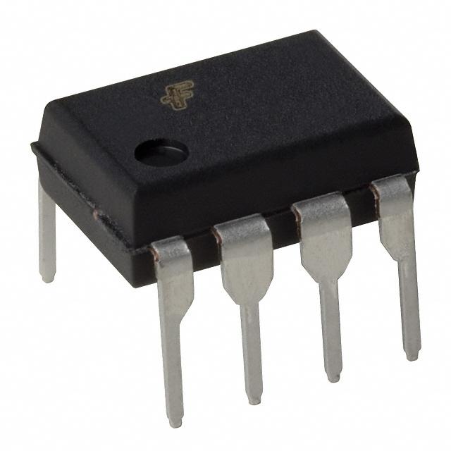
| 产品图片 |
|
| rohs | 符合RoHS无铅 / 符合限制有害物质指令(RoHS)规范要求 |
| 产品系列 | 门驱动器,Silicon Labs Si8232BB-B-IS- |
| 数据手册 | |
| 产品型号 | Si8232BB-B-ISSI8232BB-B-IS |
| 上升/下降时间(典型值) | 20ns, 20ns (最小值) |
| 上升时间 | 20 ns |
| 下降时间 | 20 ns |
| 产品 | Driver ICs - Various |
| 产品目录页面 | |
| 产品种类 | 门驱动器 |
| 传播延迟tpLH/tpHL(最大值) | 60ns, 60ns |
| 传播延迟时间 | 30 ns |
| 供应商器件封装 | 16-SOIC W |
| 共模瞬态抗扰度(最小值) | 20kV/µs |
| 关闭 | Yes |
| 其它名称 | 336-1910-5 |
| 功率耗散 | 1.2 W |
| 包装 | 管件 |
| 单位重量 | 508.350 mg |
| 商标 | Silicon Labs |
| 安装类型 | 表面贴装 |
| 安装风格 | SMD/SMT |
| 封装 | Tube |
| 封装/外壳 | 16-SOIC(0.295",7.50mm 宽) |
| 封装/箱体 | SOIC-16 Wide |
| 工作温度 | -40°C ~ 125°C |
| 工厂包装数量 | 46 |
| 延迟时间 | 60ns |
| 技术 | 容性耦合 |
| 最大功率耗散 | 1.2 W |
| 最大工作温度 | + 125 C |
| 最小工作温度 | - 40 C |
| 标准包装 | 46 |
| 激励器数量 | 2 Driver |
| 特色产品 | http://www.digikey.com/cn/zh/ph/silabs/Si82xx.html |
| 电压-正向(Vf)(典型值) | - |
| 电压-电源 | 4.5 V ~ 5.5 V |
| 电压-隔离 | 2500Vrms |
| 电流-DC正向(If) | - |
| 电流-峰值 | 500mA |
| 电流-峰值输出 | - |
| 电流-输出高,低 | - |
| 电源电压-最大 | 24 V |
| 电源电压-最小 | 6.5 V |
| 电源电流 | 3.5 mA |
| 类型 | High Side/Low Side |
| 系列 | Si8232BB |
| 绝缘电压 | 2.5 kVrms |
| 脉宽失真(最大) | 5.6ns |
| 认可 | CQC, CSA, UR, VDE |
| 输入类型 | 非反相 |
| 输出数 | 2 |
| 输出电压 | +/- 0.04 V |
| 输出电流 | 0.5 A |
| 输出端数量 | 2 |
| 通道数 | 2 |
| 通道数量 | 2 Channel |
| 配置 | Dual Driver高端或低端 |
| 配置数 | 2 |
| 高压侧电压-最大值(自举) | - |


- 商务部:美国ITC正式对集成电路等产品启动337调查
- 曝三星4nm工艺存在良率问题 高通将骁龙8 Gen1或转产台积电
- 太阳诱电将投资9.5亿元在常州建新厂生产MLCC 预计2023年完工
- 英特尔发布欧洲新工厂建设计划 深化IDM 2.0 战略
- 台积电先进制程称霸业界 有大客户加持明年业绩稳了
- 达到5530亿美元!SIA预计今年全球半导体销售额将创下新高
- 英特尔拟将自动驾驶子公司Mobileye上市 估值或超500亿美元
- 三星加码芯片和SET,合并消费电子和移动部门,撤换高东真等 CEO
- 三星电子宣布重大人事变动 还合并消费电子和移动部门
- 海关总署:前11个月进口集成电路产品价值2.52万亿元 增长14.8%

.jpg)

PDF Datasheet 数据手册内容提取
Si823x 0.5 AND 4.0 AMP ISODRIVERS (2.5 AND 5 KV ) RMS Features Two completely isolated drivers 60ns propagation delay (max) in one package Independent HS and LS inputs or Up to 5kVRMS input-to-output PWM input versions isolation Transient immunity >45kV/µs Up to 1500VDC peak driver-to- Overlap protection and driver differential voltage programmable dead time HS/LS and dual driver versions AEC-Q100 qualification Up to 8MHz switching frequency Wide operating range 0.5A peak output (Si8230/1/2/7) –40 to +125°C 4.0A peak output RoHS-compliant packages (Si8233/4/5/6/8) SOIC-16 wide body High electromagnetic immunity SOIC-16 narrow body LGA-14 Applications Power delivery systems Lighting control systems Motor control systems Plasma displays Isolated dc-dc power supplies Solar and industrial inverters Safety Approval UL 1577 recognized VDE certification conformity Up to 5000Vrms for 1 minute IEC 60747-5-5 (VDE 0884 Part 5) CSA component notice 5A EN 60950-1 (reinforced approval insulation) IEC 60950-1, 61010-1, 60601-1 CQC certification approval (reinforced insulation) GB4943.1 Ordering Information: Description See page39. The Si823x isolated driver family combines two independent, isolated drivers into a single package. The Si8230/1/3/4 are high-side/low-side drivers, and the Si8232/5/6/7/8 are dual drivers. Versions with peak output currents of 0.5A (Si8230/1/2/7) and 4.0A (Si8233/4/5/6/8) are available. All drivers operate with a maximum supply voltage of 24V. The Si823x drivers utilize Silicon Labs' proprietary silicon isolation technology, which provides up to 5kV withstand voltage per UL1577 RMS and fast 60ns propagation times. Driver outputs can be grounded to the same or separate grounds or connected to a positive or negative voltage. The TTL level compatible inputs with >400mV hysteresis are available in individual control input (Si8230/2/3/5/6/7/8) or PWM input (Si8231/4) configurations. High integration, low propagation delay, small installed size, flexibility, and cost-effectiveness make the Si823x family ideal for a wide range of isolated MOSFET/IGBT gate drive applications. Rev. 1.5 3/14 Copyright © 2014 by Silicon Laboratories Si823x
Si823x 2 Rev. 1.5
Si823x TABLE OF CONTENTS Section Page 1. Top-Level Block Diagrams . . . . . . . . . . . . . . . . . . . . . . . . . . . . . . . . . . . . . . . . . . . . . . . . .4 2. Electrical Specifications . . . . . . . . . . . . . . . . . . . . . . . . . . . . . . . . . . . . . . . . . . . . . . . . . . .6 2.1. Test Circuits . . . . . . . . . . . . . . . . . . . . . . . . . . . . . . . . . . . . . . . . . . . . . . . . . . . . . . . .9 3. Functional Description . . . . . . . . . . . . . . . . . . . . . . . . . . . . . . . . . . . . . . . . . . . . . . . . . . .16 3.1. Typical Operating Characteristics (0.5 Amp) . . . . . . . . . . . . . . . . . . . . . . . . . . . . . .17 3.2. Typical Operating Characteristics (4.0 Amp) . . . . . . . . . . . . . . . . . . . . . . . . . . . . . .19 3.3. Family Overview and Logic Operation During Startup . . . . . . . . . . . . . . . . . . . . . . .21 3.4. Power Supply Connections . . . . . . . . . . . . . . . . . . . . . . . . . . . . . . . . . . . . . . . . . . . .23 3.5. Power Dissipation Considerations . . . . . . . . . . . . . . . . . . . . . . . . . . . . . . . . . . . . . .23 3.6. Layout Considerations . . . . . . . . . . . . . . . . . . . . . . . . . . . . . . . . . . . . . . . . . . . . . . .26 3.7. Undervoltage Lockout Operation . . . . . . . . . . . . . . . . . . . . . . . . . . . . . . . . . . . . . . .26 3.8. Programmable Dead Time and Overlap Protection . . . . . . . . . . . . . . . . . . . . . . . . .28 4. Applications . . . . . . . . . . . . . . . . . . . . . . . . . . . . . . . . . . . . . . . . . . . . . . . . . . . . . . . . . . . .30 4.1. High-Side/Low-Side Driver . . . . . . . . . . . . . . . . . . . . . . . . . . . . . . . . . . . . . . . . . . . .30 4.2. Dual Driver . . . . . . . . . . . . . . . . . . . . . . . . . . . . . . . . . . . . . . . . . . . . . . . . . . . . . . . .31 4.3. Dual Driver with Thermally Enhanced Package (Si8236) . . . . . . . . . . . . . . . . . . . . .31 5. Pin Descriptions . . . . . . . . . . . . . . . . . . . . . . . . . . . . . . . . . . . . . . . . . . . . . . . . . . . . . . . . .32 6. Ordering Guide . . . . . . . . . . . . . . . . . . . . . . . . . . . . . . . . . . . . . . . . . . . . . . . . . . . . . . . . . .39 7. Package Outline: 16-Pin Wide Body SOIC . . . . . . . . . . . . . . . . . . . . . . . . . . . . . . . . . . . .43 8. Land Pattern: 16-Pin Wide Body SOIC . . . . . . . . . . . . . . . . . . . . . . . . . . . . . . . . . . . . . . .45 9. Package Outline: 16-Pin Narrow Body SOIC . . . . . . . . . . . . . . . . . . . . . . . . . . . . . . . . . .46 10. Land Pattern: 16-Pin Narrow Body SOIC . . . . . . . . . . . . . . . . . . . . . . . . . . . . . . . . . . . .47 11. Package Outline: 14 LD LGA (5 x 5 mm) . . . . . . . . . . . . . . . . . . . . . . . . . . . . . . . . . . . .48 12. Land Pattern: 14 LD LGA . . . . . . . . . . . . . . . . . . . . . . . . . . . . . . . . . . . . . . . . . . . . . . . . .49 13. Package Outline: 14 LD LGA with Thermal Pad (5 x 5 mm) . . . . . . . . . . . . . . . . . . . . .50 14. Land Pattern: 14 LD LGA with Thermal Pad . . . . . . . . . . . . . . . . . . . . . . . . . . . . . . . . .51 15. Top Markings . . . . . . . . . . . . . . . . . . . . . . . . . . . . . . . . . . . . . . . . . . . . . . . . . . . . . . . . . .52 15.1. Si823x Top Marking (16-Pin Wide Body SOIC) . . . . . . . . . . . . . . . . . . . . . . . . . . .52 15.2. Top Marking Explanation (16-Pin Wide Body SOIC) . . . . . . . . . . . . . . . . . . . . . . .52 15.3. Si823x Top Marking (16-Pin Narrow Body SOIC) . . . . . . . . . . . . . . . . . . . . . . . . . .53 15.4. Top Marking Explanation (16-Pin Narrow Body SOIC) . . . . . . . . . . . . . . . . . . . . . .53 15.5. Si823x Top Marking (14 LD LGA) . . . . . . . . . . . . . . . . . . . . . . . . . . . . . . . . . . . . . .54 15.6. Top Marking Explanation (14 LD LGA) . . . . . . . . . . . . . . . . . . . . . . . . . . . . . . . . . .54 Document Change List . . . . . . . . . . . . . . . . . . . . . . . . . . . . . . . . . . . . . . . . . . . . . . . . . . . . .55 Contact Information . . . . . . . . . . . . . . . . . . . . . . . . . . . . . . . . . . . . . . . . . . . . . . . . . . . . . . . .56 Rev. 1.5 3
Si823x 1. Top-Level Block Diagrams VDDI VDDA VIA N O TI LA VOA O S I UVLO GNDA DT CONTROL DT OVE&RLAP PROTECTION VDDI VDDI VDDI VDDB UVLO ON TI LA VOB O S I UVLO DISABLE GNDB VIB GNDI Si8230/3 Figure 1. Si8230/3 Two-Input High-Side/Low-Side Isolated Drivers VDDI VDDA PWM N O LPWM TI LA VOA O S I UVLO GNDA DT CONTROL & DT OVERLAP PROTECTION VDDI VDDI VDDI VDDB UVLO ON TI LA VOB O S I UVLO DISABLE GNDB LPWM GNDI Si8231/4 Figure 2. Si8231/4 Single-Input High-Side/Low-Side Isolated Drivers 4 Rev. 1.5
Si823x VDDI VDDA N O VIA LATI VOA O S I UVLO GNDA VDDI VDDI UVLO VDDI VDDB N O DISABLE LATI VOB O S I UVLO GNDB VIB GNDI Si8232/5/6/7/8 Figure 3. Si8232/5/6/7/8 Dual Isolated Drivers Rev. 1.5 5
Si823x 2. Electrical Specifications Table 1. Electrical Characteristics1 2.7V < VDDI < 5.5V, VDDA=VDDB=12V or 15V. TA=–40 to +125°C. Typical specs at 25°C Parameter Symbol Test Condition Min Typ Max Unit DC Specifications Input-side Power Supply Si8230/1/2/3/4/5/6 4.5 — 5.5 VDDI V Voltage Si8237/8 2.7 — 5.5 Voltage between VDDA and Driver Supply Voltage VDDA, VDDB GNDA, and VDDB and GNDB 6.5 — 24 V (See “6. Ordering Guide” ) Si8230/2/3/5/6/7/8 — 2 3 mA Input Supply Quiescent IDDI(Q) Current Si8231/4 — 3.5 5 mA Output Supply Quiescent IDDA(Q), Current per channel — — 3.0 mA Current IDDB(Q) Input Supply Active Current IDDI Input freq=500kHz, no load — 3.5 — mA IDDA Current per channel with Output Supply Active Current — 6 — mA IDDB Input freq=500kHz, no load IVIA, IVIB, Input Pin Leakage Current –10 — +10 µA dc IPWM Input Pin Leakage Current IDISABLE –10 — +10 µA dc Logic High Input Threshold VIH 2.0 — — V Logic Low Input Threshold VIL — — 0.8 V Input Hysteresis VIHYST Si8230/1/2/3/4/5/6/7/8 400 450 — mV (VDDA VOAH, Logic High Output Voltage IOA, IOB=–1mA /VDDB) — — V VOBH — 0.04 Logic Low Output Voltage VOAL, VOBL IOA, IOB=1mA — — 0.04 V Si8230/1/2/7, Figure4 — 0.5 — A Output Short-Circuit Pulsed IOA(SCL), Sink Current IOB(SCL) Si8233/4/5/6/8, Figure4 — 4.0 — A Si8230/1/2/7, Figure5 — 0.25 — A Output Short-Circuit Pulsed IOA(SCH), Source Current IOB(SCH) Si8233/4/5/6/8, Figure5 — 2.0 — A Si8230/1/2/7 — 5.0 — Output Sink Resistance RON(SINK) Si8233/4/5/6/8 — 1.0 — Notes: 1. VDDA=VDDB=12V for 5, 8, and 10V UVLO devices; VDDA=VDDB=15V for 12.5V UVLO devices. 2. TDD is the minimum overlap time without triggering overlap protection (Si8230/1/3/4 only). 3. The largest RDT resistor that can be used is 220k.. 6 Rev. 1.5
Si823x Table 1. Electrical Characteristics1 (Continued) 2.7V < VDDI < 5.5V, VDDA=VDDB=12V or 15V. TA=–40 to +125°C. Typical specs at 25°C Parameter Symbol Test Condition Min Typ Max Unit Si8230/1/2/7 — 15 — Output Source Resistance R ON(SOURCE) Si8233/4/5/6/8 — 2.7 — VDDI rising VDDI Undervoltage Threshold VDDI 3.60 4.0 4.45 V UV+ (Si8230/1/2/3/4/5/6) VDDI falling VDDI Undervoltage Threshold VDDIUV– (Si8230/1/2/3/4/5/6) 3.30 3.70 4.15 V VDDI Lockout Hysteresis VDDIHYS (Si8230/1/2/3/4/5/6) — 250 — mV VDDI Undervoltage Threshold VDDIUV+ VDDI rising (Si8237/8) 2.15 2.3 2.5 V VDDI Undervoltage Threshold VDDI VDDI falling (Si8237/8) 2.10 2.22 2.40 V UV– VDDI Lockout Hysteresis VDDIHYS (Si8237/8) — 75 — mV VDDA, VDDB Undervoltage VDDAUV+, VDDA, VDDB rising Threshold VDDBUV+ 5V Threshold See Figure37 on page 27. 5.20 5.80 6.30 V 8V Threshold See Figure38 on page 27. 7.50 8.60 9.40 V 10V Threshold See Figure39 on page 27. 9.60 11.1 12.2 V 12.5V Threshold See Figure40 on page 27. 12.4 13.8 14.8 V VDDA, VDDB Undervoltage VDDA , UV– VDDA, VDDB falling Threshold VDDBUV– 5V Threshold See Figure37 on page 27. 4.90 5.52 6.0 V 8V Threshold See Figure38 on page 27. 7.20 8.10 8.70 V 10V Threshold See Figure39 on page 27. 9.40 10.1 10.9 V 12.5V Threshold See Figure40 on page 27. 11.6 12.8 13.8 V VDDA, VDDB VDDAHYS, UVLO voltage=5V — 280 — mV Lockout Hysteresis VDDBHYS VDDA, VDDB VDDAHYS, UVLO voltage=8V — 600 — mV Lockout Hysteresis VDDBHYS VDDA, VDDB VDDAHYS, UVLO voltage=10V or 12.5V — 1000 — mV Lockout Hysteresis VDDBHYS Notes: 1. VDDA=VDDB=12V for 5, 8, and 10V UVLO devices; VDDA=VDDB=15V for 12.5V UVLO devices. 2. TDD is the minimum overlap time without triggering overlap protection (Si8230/1/3/4 only). 3. The largest RDT resistor that can be used is 220k.. Rev. 1.5 7
Si823x Table 1. Electrical Characteristics1 (Continued) 2.7V < VDDI < 5.5V, VDDA=VDDB=12V or 15V. TA=–40 to +125°C. Typical specs at 25°C Parameter Symbol Test Condition Min Typ Max Unit AC Specifications Minimum Pulse Width — 10 — ns Propagation Delay t , t CL=200pF — 30 60 ns PHL PLH Pulse Width Distortion PWD — — 5.60 ns |t -t | PLH PHL Minimum Overlap Time2 TDD DT=VDDI, No-Connect — 0.4 — ns Figure42, RDT=100k — 900 — ns Programmed Dead Time3 DT Figure42, RDT=6k — 70 — ns CL=200pF (Si8230/1/2/7) — — 20 ns Output Rise and Fall Time tR,tF CL=200pF (Si8233/4/5/6/8) — — 12 ns Shutdown Time from Disable True tSD — — 60 ns Restart Time from Disable False tRESTART — — 60 ns Time from VDD_=VDD_UV+ Device Start-up Time t — — 40 µs START to VOA, VOB=VIA, VIB Common Mode VIA, VIB, PWM=VDDI or 0V CMTI 20 45 — kV/µs Transient Immunity VCM=1500V (see Figure6) Notes: 1. VDDA=VDDB=12V for 5, 8, and 10V UVLO devices; VDDA=VDDB=15V for 12.5V UVLO devices. 2. TDD is the minimum overlap time without triggering overlap protection (Si8230/1/3/4 only). 3. The largest RDT resistor that can be used is 220k.. 8 Rev. 1.5
Si823x 2.1. Test Circuits Figures 4, 5, and 6 depict sink current, source current, and common-mode transient immunity test circuits, respectively. VDDA = VDDB = 15 V VDDI VDD 10 IN OUT INPUT Si823x SCHOTTKY + VSS 1 µF 100 µF 8 V _ 1 µF 10 µF Measure CER EL RSNS 50 ns 0.1 VDDI GND 200 ns INPUT WAVEFORM Figure 4. IOL Sink Current Test Circuit VDDA = VDDB = 15 V VDDI VDD 10 IN OUT INPUT Si823x SCHOTTKY VSS 1 µF 100 µF 5.5 V +_ 1 µF 10 µF Measure CER EL RSNS 50 ns 0.1 VDDI GND 200 ns INPUT WAVEFORM Figure 5. IOH Source Current Test Circuit Rev. 1.5 9
Si823x 12 V Supply Si823x VDDI VDDA Input Signal INPUT VOA Switch 5V DISABLE GNDA Isolated Supply DT VDDB Oscilloscope 100k VOB GNDI GNDB Isolated Ground High Voltage Output Differential Input Probe Vcm Surge Output High Voltage Surge Generator Figure 6. Common Mode Transient Immunity Test Circuit 10 Rev. 1.5
Si823x Table 2. Regulatory Information1,2,3,4 CSA The Si823x is certified under CSA Component Acceptance Notice 5A. For more details, see File 232873. 61010-1: Up to 600V reinforced insulation working voltage; up to 600V basic insulation working voltage. RMS RMS 60950-1: Up to 600V reinforced insulation working voltage; up to 1000V basic insulation working volt- RMS RMS age. 60601-1: Up to 125V reinforced insulation working voltage; up to 380V basic insulation working voltage. RMS RMS VDE The Si823x is certified according to IEC 60747-5-5. For more details, see File 5006301-4880-0001. 60747-5-5: Up to 891 V for basic insulation working voltage. peak 60950-1: Up to 600V reinforced insulation working voltage; up to 1000V basic insulation working volt- RMS RMS age. UL The Si823x is certified under UL1577 component recognition program. For more details, see File E257455. Rated up to 5000V isolation voltage for basic protection. RMS CQC The Si823x is certified under GB4943.1-2011. For more details, see File V2012CQC001041. Rated up to 600V reinforced insulation working voltage; up to 1000V basic insulation working voltage. RMS RMS Notes: 1. Regulatory Certifications apply to 2.5kV rated devices which are production tested to 3.0kV for 1sec. RMS RMS 2. Regulatory Certifications apply to 3.75kV rated devices which are production tested to 4.5kV for 1sec. RMS RMS 3. Regulatory Certifications apply to 5.0kV rated devices which are production tested to 6.0kV for 1sec. RMS RMS 4. For more information, see "6. Ordering Guide" on page 39. Rev. 1.5 11
Si823x Table 3. Insulation and Safety-Related Specifications Value 14 LD Test WBSOIC-16 14 LD Parameter Symbol WBSOIC-16 LGA with Unit Condition NBSOIC-16 LGA 5kV Pad RMS 2.5kV 2.5kV RMS RMS 1.0kV RMS Nominal Air Gap L(1O1) 8.0 8.0/4.01 3.5 1.75 mm (Clearance)1 Nominal External Tracking L(1O2) 8.0 8.0/4.01 3.5 1.75 mm (Creepage)1 Minimum Internal Gap 0.014 0.014 0.014 0.014 mm (Internal Clearance) Tracking Resistance PTI IEC60112 600 600 600 600 V (Proof Tracking Index) Erosion Depth ED 0.040 0.019 0.021 0.021 mm Resistance R 1012 1012 1012 1012 (Input-Output)2 IO Capacitance C f=1MHz 1.4 1.4 1.4 1.4 pF (Input-Output)2 IO Input Capacitance3 C 4.0 4.0 4.0 4.0 pF I Notes: 1. The values in this table correspond to the nominal creepage and clearance values as detailed in “7. Package Outline: 16-Pin Wide Body SOIC” , “9. Package Outline: 16-Pin Narrow Body SOIC” , “11. Package Outline: 14 LD LGA (5x5mm)” , and “13. Package Outline: 14 LD LGA with Thermal Pad (5x5mm)” . VDE certifies the clearance and creepage limits as 4.7mm minimum for the NB SOIC-16 and 8.5mm minimum for the WB SOIC-16 package. UL does not impose a clearance and creepage minimum for component level certifications. CSA certifies the clearance and creepage limits as 3.9mm minimum for the NB SOIC 16 and 7.6mm minimum for the WB SOIC-16 package. 2. To determine resistance and capacitance, the Si823x is converted into a 2-terminal device. Pins 1–8 (1-7, 14 LD LGA) are shorted together to form the first terminal and pins 9–16 (8-14, 14 LD LGA) are shorted together to form the second terminal. The parameters are then measured between these two terminals. 3. Measured from input pin to ground. Table 4. IEC 60664-1 (VDE 0884 Part 5) Ratings Specification Parameter Test Condition 14 LD WB NB 14 LD LGA SOIC-16 SOIC-16 LGA with Pad Basic Isolation Group Material Group I I I I Rated Mains Voltages < 150V I-IV I-IV I-IV I-IV RMS Rated Mains Voltages < 300V I-IV I-III I-III I-III RMS Installation Classification Rated Mains Voltages < 400V I-III I-II I-II I-II RMS Rated Mains Voltages < 600V I-III I-II I-II I-I RMS 12 Rev. 1.5
Si823x Table 5. IEC 60747-5-5 Insulation Characteristics* Characteristic Parameter Symbol Test Condition WB NB SOIC-16 14 LD LGA Unit SOIC-16 14 LD LGA with Pad Maximum Working Insulation V 891 560 373 V peak Voltage IORM Method b1 (V x1.875=V , IORM PR 100% Input to Output Test Voltage V Production Test, 1375 1050 700 V peak PR t =1 sec, m Partial Discharge < 5 pC) Transient Overvoltage V t=60sec 6000 4000 2650 V peak IOTM Pollution Degree (DIN VDE 2 2 2 0110, Table 1) Insulation Resistance at TS, R >109 >109 >109 V =500V S IO *Note: Maintenance of the safety data is ensured by protective circuits. The Si823x provides a climate classification of 40/125/21. Table 6. IEC Safety Limiting Values1 14 LD WB NB 14 LD Parameter Symbol Test Condition LGA with Unit SOIC-16 SOIC-16 LGA Pad Case T 150 150 150 150 °C Temperature S =100°C/W (WB SOIC-16), JA 105°C/W (NB SOIC-16, 14 LD LGA), Safety Input 50°C/W (14 LD LGA with Pad) I 50 50 50 100 mA Current S V =5.5V, DDI V =V =24V, DDA DDB T =150°C, T =25°C J A Device Power P 1.2 1.2 1.2 1.2 W Dissipation2 D Notes: 1. Maximum value allowed in the event of a failure. Refer to the thermal derating curve in Figures 7 and 8. 2. The Si82xx is tested with V =5.5V, V =V =24V, T =150ºC, C =100pF, input 2MHz 50% duty cycle DDI DDA DDB J L square wave. Rev. 1.5 13
Si823x Table 7. Thermal Characteristics 14 LD WB NB 14 LD Parameter Symbol LGA with Unit SOIC-16 SOIC-16 LGA Pad IC Junction-to-Air 100 105 105 50 °C/W Thermal Resistance JA Table 8. Absolute Maximum Ratings1 Parameter Symbol Min Typ Max Unit Storage Temperature2 T –65 — +150 °C STG Ambient Temperature under Bias T –40 — +125 °C A Junction Temperature T — — +150 °C J Input-side Supply Voltage VDDI –0.6 — 6.0 V Driver-side Supply Voltage VDDA, VDDB –0.6 — 30 V Voltage on any Pin with respect to Ground VIN –0.5 — VDD + 0.5 V Output Drive Current per Channel I — — 10 mA O Lead Solder Temperature (10sec.) — — 260 °C Maximum Isolation (Input to Output) (1sec) — — 6500 V WB SOIC-16 RMS Maximum Isolation (Output to Output) (1sec) — — 2500 V WB SOIC-16 RMS Maximum Isolation (Input to Output) (1sec) — — 4250 V NB SOIC-16 RMS Maximum Isolation (Output to Output) (1sec) — — 2500 V NB SOIC-16 RMS Maximum Isolation (Input to Output) (1sec) — — 3850 V 14 LD LGA without Thermal Pad RMS Maximum Isolation (Output to Output) (1sec) — — 650 V 14 LD LGA without Thermal Pad RMS Maximum Isolation (Input to Output) (1sec) — — 1850 V 14 LD LGA with Thermal Pad RMS Maximum Isolation (Output to Output) (1sec) — — 0 V 14 LD LGA with Thermal Pad RMS Notes: 1. Permanent device damage may occur if the absolute maximum ratings are exceeded. Functional operation should be restricted to the conditions as specified in the operational sections of this data sheet. Exposure to absolute maximum rating conditions for extended periods may affect device reliability. 2. VDE certifies storage temperature from –40 to 150°C. 14 Rev. 1.5
Si823x 60 ) A m ( 50 t n e VDDI = 5.5 V r 40 ur VDDA, VDDB = 24 V C 30 g n ti mi 20 Li y- 10 t e f a 0 S 0 50 100 150 200 Case Temperature (ºC) Figure 7. WB SOIC-16, NB SOIC-16, 14 LD LGA Thermal Derating Curve, Dependence of Safety Limiting Values with Case Temperature per DIN EN 60747-5-5 120 ) A m VDDI = 5.5 V ( 100 VDDA, VDDB = 24 V t n e r 80 r u C 60 g n ti mi 40 Li y- 20 t e f a 0 S 0 50 100 150 200 Case Temperature (ºC) Figure 8. 14 LD LGA with Pad Thermal Derating Curve, Dependence of Safety Limiting Values with Case Temperature per DIN EN 60747-5-5 Rev. 1.5 15
Si823x 3. Functional Description The operation of an Si823x channel is analogous to that of an optocoupler and gate driver, except an RF carrier is modulated instead of light. This simple architecture provides a robust isolated data path and requires no special considerations or initialization at start-up. A simplified block diagram for a single Si823x channel is shown in Figure9. Transmitter Receiver Driver RF OSCILLATOR V DD Semiconductor- Dead A time MODULATOR Based Isolation DEMODULATOR B Barrier control 0.5 to 4 A peak Gnd Figure 9. Simplified Channel Diagram A channel consists of an RF Transmitter and RF Receiver separated by a semiconductor-based isolation barrier. Referring to the Transmitter, input A modulates the carrier provided by an RF oscillator using on/off keying. The Receiver contains a demodulator that decodes the input state according to its RF energy content and applies the result to output B via the output driver. This RF on/off keying scheme is superior to pulse code schemes as it provides best-in-class noise immunity, low power consumption, and better immunity to magnetic fields. See Figure10 for more details. Input Signal Modulation Signal Output Signal Figure 10. Modulation Scheme 16 Rev. 1.5
Si823x 3.1. Typical Operating Characteristics (0.5 Amp) The typical performance characteristics depicted in Figures 11 through 22 are for information purposes only. Refer to Table1 on page6 for actual specification limits. 10 7 8 mA)6 DCut=y 1C0y0c lpeF = 50% 1MHz ns) Tfall nt (5 1 LChannel Switching me ( 6 urre4 500kHz Fall Ti 4 Trise pply C3 100kHz se/ Su2 Ri 2 VDD=12V, 25°C VDDA 01 50 kHz C = 100 pF L 9 14 19 24 0 VDDA Supply Voltage (V) 9 12 15 18 21 24 VDDA Supply (V) Figure 14. Supply Current vs. Supply Voltage Figure 11. Rise/Fall Time vs. Supply Voltage 30 5 ns) 25 A) y ( m4 opagation Dela 1250 HL--LH pply Current (23 VfD =Du tD2y5 AC0 y=kcH 1lez5 ,V =C, 5L0=% 0 pF Pr VDD=12V, 25°C Su 2 Channels Switching C = 100 pF 1 L 10 -50 0 50 100 9 12 15 18 21 24 Temperature (°C) VDDA Supply (V) Figure 15. Supply Current vs. Temperature Figure 12. Propagation Delay vs. Supply Voltage 40 35 Trise mA) 3.45 DCuLt=y 0C ypcFle = 50% e (ns) 2350 y Current ( 2.35 1 Channel Switching 1MHz500kHz se/Fall Tim 1250 Tfall pl Ri 10 up 2 100kHz S 5 DA 1.5 VDD=12V, 25°C D 50 kHz 0 V 1 0.0 0.5 1.0 1.5 2.0 9 14 19 24 Load (nF) VDDA Supply Voltage (V) Figure 16. Rise/Fall Time vs. Load Figure 13. Supply Current vs. Supply Voltage Rev. 1.5 17
Si823x 50 4(cid:1011)(cid:1009) 45 (cid:1008)(cid:1009)(cid:1004) ns) 40 (cid:36)(cid:12) (cid:1008)(cid:1006)(cid:1009) n Delay ( 3305 L-H (cid:88)(cid:85)(cid:85)(cid:72)(cid:81)(cid:87)(cid:3)(cid:11)(cid:80) (cid:1008)(cid:1007)(cid:1004)(cid:1011)(cid:1004)(cid:1009) o (cid:38) agati 25 H-L (cid:88)(cid:85)(cid:70)(cid:72)(cid:3) (cid:1007)(cid:1009)(cid:1004) Prop 20 (cid:54)(cid:82) (cid:1007)(cid:1006)(cid:1009) 15 (cid:1007)(cid:1004)(cid:1004) VDD=12V, 25°C VDD=12V, Vout=VDD-5V 10 (cid:1006)(cid:1011)(cid:1009) 0.0 0.5 1.0 1.5 2.0 10 15 20 25 Load (nF) (cid:54)(cid:88)(cid:83)(cid:83)(cid:79)(cid:92)(cid:3)(cid:57)(cid:82)(cid:79)(cid:87)(cid:68)(cid:74)(cid:72)(cid:3)(cid:11)(cid:57)(cid:12) Figure 17. Propagation Delay vs. Load Figure 20. Output Source Current vs. Supply Voltage 30 (cid:1012)(cid:1009)(cid:1004) ns) 25 (cid:1012)(cid:1006)(cid:1009) y ( L-H (cid:1012)(cid:1004)(cid:1004) Dela (cid:80)(cid:36)(cid:12) (cid:1011)(cid:1011)(cid:1011)(cid:1009)(cid:1009)(cid:1004) on 20 H-L (cid:81)(cid:87)(cid:3)(cid:11) 7(cid:1006)(cid:1009) gati (cid:88)(cid:85)(cid:85)(cid:72) (cid:1011)(cid:1004)(cid:1004) Propa 15 (cid:54)(cid:76)(cid:81)(cid:78)(cid:3)(cid:38) (cid:1010)(cid:1010)(cid:1011)(cid:1009)(cid:1009)(cid:1004) (cid:1010)(cid:1006)(cid:1009) VDD=12V, Load = 200pF (cid:1010)(cid:1004)(cid:1004) 10 (cid:1009)(cid:1011)(cid:1009) VDD=12V, Vout=5V -40 -20 0 20 40 60 80 100 120 (cid:1009)(cid:1009)(cid:1004) Temperature (°C) -40 -10 20 50 80 110 Figure 18. Propagation Delay vs. Temperature (cid:55)(cid:72)(cid:80)(cid:83)(cid:72)(cid:85)(cid:68)(cid:87)(cid:88)(cid:85)(cid:72)(cid:3)(cid:11)°(cid:38)(cid:12) Figure 21. Output Sink Current vs. Temperature (cid:1005)(cid:1005)(cid:1006)(cid:1009) (cid:1008)(cid:1006)5 (cid:1005)(cid:1004)(cid:1004)(cid:1004) (cid:1008)(cid:1004)(cid:1004) (cid:36)(cid:12) (cid:36)(cid:12) (cid:54)(cid:76)(cid:81)(cid:78)(cid:3)(cid:38)(cid:88)(cid:85)(cid:85)(cid:72)(cid:81)(cid:87)(cid:3)(cid:11)(cid:80) (cid:1011)(cid:1012)(cid:1010)(cid:1009)(cid:1011)(cid:1006)(cid:1004)(cid:1009)(cid:1009) (cid:82)(cid:88)(cid:85)(cid:70)(cid:72)(cid:3)(cid:38)(cid:88)(cid:85)(cid:85)(cid:72)(cid:81)(cid:87)(cid:3)(cid:11)(cid:80) (cid:1007)(cid:1007)3(cid:1009)(cid:1006)(cid:1011)(cid:1004)5(cid:1009) (cid:54) VDD=12V, Vout=5V (cid:1007)(cid:1004)(cid:1004) (cid:1009)(cid:1004)(cid:1004) 10 12 14 16 18 20 22 24 VDD=12V, Vout=VDD-5V (cid:1006)(cid:1011)(cid:1009) (cid:54)(cid:88)(cid:83)(cid:83)(cid:79)(cid:92)(cid:3)(cid:57)(cid:82)(cid:79)(cid:87)(cid:68)(cid:74)(cid:72)(cid:3)(cid:11)(cid:57)(cid:12) -40 -10 20 50 80 110 Figure 19. Output Sink Current vs. Supply (cid:55)(cid:72)(cid:80)(cid:83)(cid:72)(cid:85)(cid:68)(cid:87)(cid:88)(cid:85)(cid:72)(cid:3)(cid:11)°(cid:38)(cid:12) Voltage Figure 22. Output Source Current vs. Temperature 18 Rev. 1.5
Si823x 3.2. Typical Operating Characteristics (4.0 Amp) The typical performance characteristics depicted in Figures 23 through 34 are for information purposes only. Refer to Table1 on page6 for actual specification limits. 10 A)14 Duty Cycle = 50% 8 nt (m12 C1 LC=h a1n0n0e pl FSwitching 1MHz se/Fall Time (ns) 46 Tfall Trise DDA Supply Curre102468 500kHz 15000 kkHHzz Ri V 0 2 9 14 19 24 VDD=12V, 25°C VDDA Supply Voltage (V) C = 100 pF L 0 Figure 26. Supply Current vs. Supply Voltage 9 12 15 18 21 24 VDDA Supply (V) 10 Figure 23. Rise/Fall Time vs. Supply Voltage A) 8 m 30 nt ( 6 e Curr 4 VDDA = 15V, elay (ns) 25 L-H Supply 2 fD2 = uC t2hy5 aC0nykncHelelzs , =SC 5wL0i=t%c 0h ipnFg n D 20 0 o -50 0 50 100 ati ag H-L Temperature (°C) p o 15 Pr Figure 27. Supply Current vs. Temperature VDD=12V, 25°C C = 100 pF L 10 40 9 12 15 18 21 24 35 VDDA Supply (V) Trise 30 Figure 24. Propagation Delay vs. Supply ns) Voltage me ( 25 all Ti 20 Tfall F 15 e/ s A) 14 Duty Cycle = 50% Ri 10 Current (m 11028 C1 LC=h a0n pnFel Switching 1MHz 05 VDD=12V, 25°C y 500kHz 0 1 2 3 4 5 6 7 8 9 10 pl 6 p Su 4 100kHz Load (nF) A D 2 D Figure 28. Rise/Fall Time vs. Load V 50 kHz 0 9 14 19 24 VDDA Supply Voltage (V) Figure 25. Supply Current vs. Supply Voltage Rev. 1.5 19
Si823x 50 4 45 3.75 H-L s) 40 3.5 ay (n 35 nt (A) 3.25 n Del 30 L-H Curre 3 pagatio 25 Source 2.27.55 o 20 Pr 2.25 15 VDD=12V, Vout=VDD-5V 2 VDD=12V, 25°C 10 10 15 20 25 0 1 2 3 4 5 6 7 8 9 10 Supply Voltage (V) Load (nF) Figure 32. Output Source Current vs. Supply Figure 29. Propagation Delay vs. Load Voltage 30 7 6.75 s) 25 H-L 6.5 ay (n A) 6.265 Del L-H nt ( 5.75 gation 20 k Curre 5.52.55 a n 5 op 15 Si 4.75 Pr 4.5 VDD=12V, Load = 200pF 4.25 VDD=12V, Vout=5V 10 4 -40 -20 0 20 40 60 80 100 120 -40 -10 20 50 80 110 Temperature (°C) Temperature (°C) Figure 30. Propagation Delay vs. Temperature Figure 33. Output Sink Current vs. Temperature 3.5 9 3.25 8 A) nk Current (A) 67 urce Current ( 2.27.553 Si o S 5 2.25 VDD=12V, Vout=5V VDD=12V, Vout=VDD-5V 4 2 10 12 14 16 18 20 22 24 -40 -10 20 50 80 110 Supply Voltage (V) Temperature (°C) Figure 31. Output Sink Current vs. Supply Figure 34. Output Source Current vs. Voltage Temperature 20 Rev. 1.5
Si823x 3.3. Family Overview and Logic Operation During Startup The Si823x family of isolated drivers consists of high-side, low-side, and dual driver configurations. 3.3.1. Products Table9 shows the configuration and functional overview for each product in this family. Table 9. Si823x Family Overview Part Number Configuration Overlap Programmable Inputs Peak Output Protection Dead Time Current (A) Si8230 High-Side/Low-Side VIA, VIB 0.5 Si8231 High-Side/Low-Side PWM 0.5 Si8232/7 Dual Driver — — VIA, VIB 0.5 Si8233 High-Side/Low-Side VIA, VIB 4.0 Si8234 High-Side/Low-Side PWM 4.0 Si8235/6/8 Dual Driver — — VIA, VIB 4.0 3.3.2. Device Behavior Table10 consists of truth tables for the Si8230/3, Si8231/4, and Si8232/5/6 families. Table 10. Si823x Family Truth Table1 Si8230/3 (High-Side/Low-Side) Truth Table Inputs Output VDDI State Disable Notes VIA VIB VOA VOB Output transition occurs after internal dead time L L Powered L L L expires. Output transition occurs after internal dead time L H Powered L L H expires. Output transition occurs after internal dead time H L Powered L H L expires. Invalid state. Output transition occurs after internal H H Powered L L L dead time expires. Output returns to input state within 7µs of VDDI X2 X2 Unpowered X L L power restoration. X X Powered H L L Device is disabled. Si8231/4 (PWM Input High-Side/Low-Side) Truth Table Output PWM Input VDDI State Disable Notes VOA VOB Output transition occurs after internal dead time H Powered L H L expires. Output transition occurs after internal dead time L Powered L L H expires. Output returns to input state within 7µs of VDDI X2 Unpowered X L L power restoration. X Powered H L L Device is disabled. Notes: 1. This truth table assumes VDDA and VDDB are powered. If VDDA and VDDB are below UVLO, see "3.7.2. Undervoltage Lockout" on page 26 for more information. 2. Note that an input can power the input die through an internal diode if its source has adequate current. Rev. 1.5 21
Si823x Table 10. Si823x Family Truth Table1 (Continued) Si8232/5/6/7/8 (Dual Driver) Truth Table Inputs Output VDDI State Disable Notes VIA VIB VOA VOB Output transition occurs immediately L L Powered L L L (no internal dead time). Output transition occurs immediately L H Powered L L H (no internal dead time). Output transition occurs immediately H L Powered L H L (no internal dead time). Output transition occurs immediately H H Powered L H H (no internal dead time). Output returns to input state within 7µs of VDDI X2 X2 Unpowered X L L power restoration. X X Powered H L L Device is disabled. Notes: 1. This truth table assumes VDDA and VDDB are powered. If VDDA and VDDB are below UVLO, see "3.7.2. Undervoltage Lockout" on page 26 for more information. 2. Note that an input can power the input die through an internal diode if its source has adequate current. 22 Rev. 1.5
Si823x 3.4. Power Supply Connections Isolation requirements mandate individual supplies for VDDI, VDDA, and VDDB. The decoupling caps for these supplies must be placed as close to the VDD and GND pins of the Si823x as possible. The optimum values for these capacitors depend on load current and the distance between the chip and the regulator that powers it. Low effective series resistance (ESR) capacitors, such as Tantalum, are recommended. 3.5. Power Dissipation Considerations Proper system design must assure that the Si823x operates within safe thermal limits across the entire load range.The Si823x total power dissipation is the sum of the power dissipated by bias supply current, internal parasitic switching losses, and power dissipated by the series gate resistor and load. Equation1 shows total Si823x power dissipation. R R P =V I +2I V +fQ V ------------p-------- +fQ V ------------n-------- +2fCintV 2 D DDI DDI DD2 DD2 TL DD2 R +R TL DD2 R +R DD2 p g n g where: P is the total Si823x device power dissipation (W) D I is the input-side maximum bias current (3 mA) DDI I is the driver die maximum bias current (2.5 mA) DD2 C is the internal parasitic capacitance (75 pF for the 0.5 A driver and 370 pF for the 4.0 A driver) int V is the input-side VDD supply voltage (2.7 to 5.5 V) DDI V is the driver-side supply voltage (10 to 24 V) DD2 f is the switching frequency (Hz) Q is the total highside bootstrap charge (see Section 2.2 of AN486) TL R is the external gate resistor G R is the R of the driver pull-up switch: (Rp=15 for the 0.5A driver; Rp=2.7 for the 4.0A driver) P DSON R is the R of the driver pull-down switch: (Rn=5 for the 0.5A driver and 1 for the 4.0A driver) n DSON Equation1. Power dissipation example for 0.5 A driver using Equation 1 with the following givens: V =5.0V DDI V =12V DD2 f=350kHz R =22 G Q =25nC G Pd=0.015+0.060+3501032510–912 -------1---5--------- +fQ V -------5--------- +23501037510–12144 15+22 TL DD2 5+22 = 140 mW From which the driver junction temperature is calculated using Equation 2, where: Pd is the total Si823x device power dissipation (W) is the thermal resistance from junction to air (105 °C/W in this example) ja T is the ambient temperature A Rev. 1.5 23
Si823x T = P +T j d ja A = (0.145)(105) + 20 = 35.2 °C The maximum power dissipation allowable for the Si823x is a function of the package thermal resistance, ambient temperature, and maximum allowable junction temperature, as shown in Equation2: T –T P ----j--m----a---x------------A-- Dmax ja where: P = Maximum Si823x power dissipation (W) Dmax T = Si823x maximum junction temperature (150 °C) jmax T = Ambient temperature (°C) A ja = Si823x junction-to-air thermal resistance (105 °C/W) f = Si823x switching frequency (Hz) Equation2. Substituting values for P T , T , and into Equation2 results in a maximum allowable total power Dmax jmax A ja dissipation of 1.19W. Maximum allowable load is found by substituting this limit and the appropriate data sheet values from Table1 on page6 into Equation1 and simplifying. The result is Equation3 (0.5A driver) and Equation4 (4.0A driver), both of which assume VDDI=5V and VDDA=VDDB=18V. –3 1.410 –11 C = --------------------------–7.510 L(MAX) f Equation3. –3 1.410 –10 C = --------------------------–3.710 L(MAX) f Equation4. Equation1 and Equation2 are graphed in Figure35 where the points along the load line represent the package dissipation-limited value of CL for the corresponding switching frequency. 24 Rev. 1.5
Si823x 16,000 0.5A Driver (pF) 14,000 4A Driver (pF) 12,000 10,000 F) p d ( oa 8,000 L x a M 6,000 4,000 2,000 0 1 1 2 2 3 3 4 4 5 5 6 6 7 0 5 0 5 0 5 0 5 0 5 0 5 0 0 0 0 0 0 0 0 0 0 0 0 0 0 Frequency (Khz) Figure 35. Max Load vs. Switching Frequency Rev. 1.5 25
Si823x 3.6. Layout Considerations It is most important to minimize ringing in the drive path and noise on the Si823x VDD lines. Care must be taken to minimize parasitic inductance in these paths by locating the Si823x as close to the device it is driving as possible. In addition, the VDD supply and ground trace paths must be kept short. For this reason, the use of power and ground planes is highly recommended. A split ground plane system having separate ground and VDD planes for power devices and small signal components provides the best overall noise performance. 3.7. Undervoltage Lockout Operation Device behavior during start-up, normal operation and shutdown is shown in Figure36, where UVLO+ and UVLO- are the positive-going and negative-going thresholds respectively. Note that outputs VOA and VOB default low when input side power supply (VDDI) is not present. 3.7.1. Device Startup Outputs VOA and VOB are held low during power-up until VDD is above the UVLO threshold for time period tSTART. Following this, the outputs follow the states of inputs VIA and VIB. 3.7.2. Undervoltage Lockout Undervoltage Lockout (UVLO) is provided to prevent erroneous operation during device startup and shutdown or when VDD is below its specified operating circuits range. The input (control) side, Driver A and Driver B, each have their own undervoltage lockout monitors. The Si823x input side enters UVLO when VDDI < VDDI , and exits UVLO when VDDI > VDDI . The driver UV– UV+ outputs, VOA and VOB, remain low when the input side of the Si823x is in UVLO and their respective VDD supply (VDDA, VDDB) is within tolerance. Each driver output can enter or exit UVLO independently. For example, VOA unconditionally enters UVLO when VDDA falls below VDDA and exits UVLO when VDDA rises above UV– VDDA . UV+ UVLO+ UVLO- VDDHYS VDDI UVLO+ UVLO- VDDHYS VDDA VIA DISABLE tSD tSD tRESTART tPHL tPLH tSTART tSTART tSTART VOA Figure 36. Device Behavior during Normal Operation and Shutdown 26 Rev. 1.5
Si823x 3.7.3. Undervoltage Lockout (UVLO) The UVLO circuit unconditionally drives VO low when VDD is below the lockout threshold. Referring to Figures 37 through 40, upon power up, the Si823x is maintained in UVLO until VDD rises above VDD . During power down, UV+ the Si823x enters UVLO when VDD falls below the UVLO threshold plus hysteresis (i.e., VDD < VDD – UV+ VDD ). HYS VDDUV+ (Typ) VDDUV+ (Typ) 10.5 10.5 V)O V)O e ( e ( g g a a olt olt V V ut ut p p ut ut O O 3.5 4.0 4.5 5.0 5.5 6.0 6.5 7.0 7.5 8.5 9.0 9.5 10.0 10.5 11.0 11.5 12.0 12.5 Supply Voltage (VDD - VSS) (V) Supply Voltage (VDD - VSS) (V) Figure 37. Si823x UVLO Response (5 V) Figure 39. Si823x UVLO Response (10 V) VDDUV+ (Typ) VDDUV+ (Typ) 5 5 0. 0. 1 1 V)O V)O e ( e ( g g a a olt olt V V ut ut p p ut ut O O 6.0 6.5 7.0 7.5 8.0 8.5 9.0 9.5 10.0 11.3 11.8 12.3 12.8 13.3 13.8 14.3 14.8 15.3 Supply Voltage (VDD - VSS) (V) Supply Voltage (VDD - VSS) (V) Figure 38. Si823x UVLO Response (8 V) Figure 40. Si823x UVLO Response (12.5 V) Rev. 1.5 27
Si823x 3.7.4. Control Inputs VIA, VIB, and PWM inputs are high-true, TTL level-compatible logic inputs. A logic high signal on VIA or VIB causes the corresponding output to go high. For PWM input versions (Si8231/4), VOA is high and VOB is low when the PWM input is high, and VOA is low and VOB is high when the PWM input is low. 3.7.5. Disable Input When brought high, the DISABLE input unconditionally drives VOA and VOB low regardless of the states of VIA and VIB. Device operation terminates within tSD after DISABLE=V and resumes within tRESTART after IH DISABLE=V . The DISABLE input has no effect if VDDI is below its UVLO level (i.e., VOA, VOB remain low). IL 3.8. Programmable Dead Time and Overlap Protection All high-side/low-side drivers (Si8230/1/3/4) include programmable overlap protection to prevent outputs VOA and VOB from being high at the same time. These devices also include programmable dead time, which adds a user- programmable delay between transitions of VOA and VOB. When enabled, dead time is present on all transitions, even after overlap recovery. The amount of dead time delay (DT) is programmed by a single resistor (RDT) connected from the DT input to ground per Equation5. Note that the dead time pin can be tied to VDDI or left floating to provide a nominal dead time at approximately 400ps. DT10RDT where: DT= dead time (ns) and RDT= dead time programming resistor (k Equation5. The device driving VIA and VIB should provide a minimum dead time of TDD to avoid activating overlap protection. Input/output timing waveforms for the two-input drivers are shown in Figure41, and dead time waveforms are shown in Figure42. Ref Description VIA/ A Normal operation: VIA high, VIB low. PWM B Normal operation: VIB high, VIA low. C Contention: VIA=VIB=high. VIB D Recovery from contention: VIA transitions low. E Normal operation: VIA=VIB=low. VOA F Normal operation: VIA high, VIB low. G Contention: VIA=VIB=high. VOB H Recovery from contention: VIB transitions low. I Normal operation: VIB transitions high. A B C D E F G H I Figure 41. Input / Output Waveforms for High-Side / Low-Side Two-Input Drivers 28 Rev. 1.5
Si823x OVERLAP OVERLAP VOB VIA/ VIA/ PWM PWM 50% VIB VIB DT DT DT DT VOA 90% VOA 10% DT DT 90% VOB VOB 10% A. Typical Dead Time Operation B. Dead Time Operation During Overlap Figure 42. Dead Time Waveforms for High-Side/Low-Side Two-Input Drivers Rev. 1.5 29
Si823x 4. Applications The following examples illustrate typical circuit configurations using the Si823x. 4.1. High-Side/Low-Side Driver Figure43A shows the Si8230/3 controlled using the VIA and VIB input signals, and Figure43B shows the Si8231/4 controlled by a single PWM signal. VDDI VDD2 D1 VDDI VDD2 D1 C2 C2 VDDI 1 µF VDDI 1 µF C1 1500 V max C1 1500 V max 1uF 1uF GNDI VDDA GNDI VDDA CB CB OUT1 VIA Q1 PWMOUT PWM Q1 VOA VOA OUT2 VIB DT GNDA DT GNDA CONTROLLER RDT Si8230/3 CONTROLLER RDT Si8231/4 VDDB VDDB VDDB VDDB C3 C3 10uF 10uF I/O DISABLE I/O DISABLE GNDB GNDB Q2 Q2 VOB VOB A B Figure 43. Si823x in Half-Bridge Application For both cases, D1 and CB form a conventional bootstrap circuit that allows VOA to operate as a high-side driver for Q1, which has a maximum drain voltage of 1500V. VOB is connected as a conventional low-side driver. Note that the input side of the Si823x requires VDD in the range of 4.5 to 5.5V (2.7 to 5.5V for Si8237/8), while the VDDA and VDDB output side supplies must be between 6.5 and 24V with respect to their respective grounds. The boot-strap start up time will depend on the CB cap chosen. VDD2 is usually the same as VDDB. Also note that the bypass capacitors on the Si823x should be located as close to the chip as possible. Moreover, it is recommended that 0.1 and 10µF bypass capacitors be used to reduce high frequency noise and maximize performance. 30 Rev. 1.5
Si823x 4.2. Dual Driver Figure44 shows the Si823x configured as a dual driver. Note that the drain voltages of Q1 and Q2 can be referenced to a common ground or to different grounds with as much as 1500V dc between them. VDDI VDDI C1 Q1 VOA 10 µF GNDI VDDA PH1 VIA VDDA C2 PH2 VIB 10 µF GNDA CONTROLLER Si8232/5/7/8 VDDB VDDB C3 I/O DISABLE 10 µF GNDB Q2 VOB Figure 44. Si8232/5/7/8 in a Dual Driver Application Because each output driver resides on its own die, the relative voltage polarities of VOA and VOB can reverse without damaging the driver. That is, the voltage at VOA can be higher or lower than that of VOB by VDD without damaging the driver. Therefore, a dual driver in a low-side high side/low side drive application can use either VOA or VOB as the high side driver. Similarly, a dual driver can operate as a dual low-side or dual high-side driver and is unaffected by static or dynamic voltage polarity changes. 4.3. Dual Driver with Thermally Enhanced Package (Si8236) The thermal pad of the Si8236 must be connected to a heat spreader to lower thermal resistance. Generally, the larger the thermal shield’s area, the lower the thermal resistance. It is recommended that thermal vias also be used to add mass to the shield. Vias generally have much more mass than the shield alone and consume less space, thus reducing thermal resistance more effectively. While the heat spreader is not generally a circuit ground, it is a good reference plane for the Si8236 and is also useful as a shield layer for EMI reduction. With a 10mm2 thermal plane on the outer layers (including 20 thermal vias), the thermal impedance of the Si8236 was measured at 50°C/W. This is a significant improvement over the Si8235 which does not include a thermal pad. The Si8235’s thermal resistance was measured at 105°C /W. In addition, note that the GNDA and GNDB pins for the Si8236 are connected together through the thermal pad. Rev. 1.5 31
Si823x 5. Pin Descriptions SOIC-16 (Wide) SOIC-16 (Narrow) VIA 1 16 VDDA VIA 1 16 VDDA VIB 2 15 VOA VIB 2 15 VOA VDDI 3 14 GNDA VDDI 3 14 GNDA GNDI 4 Si8230 13 NC GNDI 4 Si823013 NC Si8233 Si8233 DISABLE 5 12 NC DISABLE 5 12 NC DT 6 11 VDDB DT 6 11 VDDB NC 7 10 VOB NC 7 10 VOB VDDI 8 9 GNDB VDDI 8 9 GNDB Table 11. Si8230/3 Two-Input HS/LS Isolated Driver (SOIC-16) Pin Name Description 1 VIA Non-inverting logic input terminal for Driver A. 2 VIB Non-inverting logic input terminal for Driver B. 3 VDDI Input-side power supply terminal; connect to a source of 4.5 to 5.5V. 4 GNDI Input-side ground terminal. 5 DISABLE Device Disable. When high, this input unconditionally drives outputs VOA, VOB LOW. It is strongly recommended that this input be connected to external logic level to avoid erroneous operation due to capacitive noise coupling. 6 DT Dead time programming input. The value of the resistor connected from DT to ground sets the dead time between output transitions of VOA and VOB. Defaults to 400ps dead time when con- nected to VDDI or left open (see "3.8. Programmable Dead Time and Overlap Protection" on page 28). 7 NC No connection. 8 VDDI Input-side power supply terminal; connect to a source of 4.5 to 5.5V. 9 GNDB Ground terminal for Driver B. 10 VOB Driver B output (low-side driver). 11 VDDB Driver B power supply voltage terminal; connect to a source of 6.5 to 24V. 12 NC No connection. 13 NC No connection. 14 GNDA Ground terminal for Driver A. 15 VOA Driver A output (high-side driver). 16 VDDA Driver A power supply voltage terminal; connect to a source of 6.5 to 24V. 32 Rev. 1.5
Si823x SOIC-16 (Wide) SOIC-16 (Narrow) PWM 1 16 VDDA PWM 1 16 VDDA NC 2 15 VOA NC 2 15 VOA VDDI 3 14 GNDA VDDI 3 14 GNDA GNDI 4 Si8231 13 NC GNDI 4 Si823113 NC Si8234 Si8234 DISABLE 5 12 NC DISABLE 5 12 NC DT 6 11 VDDB DT 6 11 VDDB NC 7 10 VOB NC 7 10 VOB VDDI 8 9 GNDB VDDI 8 9 GNDB Table 12. Si8231/4 PWM Input HS/LS Isolated Driver (SOIC-16) Pin Name Description 1 PWM PWM input. 2 NC No connection. 3 VDDI Input-side power supply terminal; connect to a source of 4.5 to 5.5V. 4 GNDI Input-side ground terminal. 5 DISABLE Device Disable. When high, this input unconditionally drives outputs VOA, VOB LOW. It is strongly recommended that this input be connected to external logic level to avoid erroneous operation due to capacitive noise coupling. 6 DT Dead time programming input. The value of the resistor connected from DT to ground sets the dead time between output transitions of VOA and VOB. Defaults to 400ps dead time when con- nected to VDDI or left open (see "3.8. Programmable Dead Time and Overlap Protection" on page 28). 7 NC No connection. 8 VDDI Input-side power supply terminal; connect to a source of 4.5 to 5.5V. 9 GNDB Ground terminal for Driver B. 10 VOB Driver B output (low-side driver). 11 VDDB Driver B power supply voltage terminal; connect to a source of 6.5 to 24V. 12 NC No connection. 13 NC No connection. 14 GNDA Ground terminal for Driver A. 15 VOA Driver A output (high-side driver). 16 VDDA Driver A power supply voltage terminal; connect to a source of 6.5 to 24V. Rev. 1.5 33
Si823x SOIC-16 (Wide) SOIC-16 (Narrow) VIA 1 16 VDDA VIA 1 16 VDDA VIB 2 15 VOA VIB 2 15 VOA VDDI 3 14 GNDA VDDI 3 Si823214 GNDA Si8232 Si8235 GNDI 4 Si8235 13 NC GNDI 4 13 NC Si8237 Si8237 DISABLE 5 12 NC DISABLE 5 Si823812 NC Si8238 NC 6 11 VDDB NC 6 11 VDDB NC 7 10 VOB NC 7 10 VOB VDDI 8 9 GNDB VDDI 8 9 GNDB Table 13. Si8232/5/7/8 Dual Isolated Driver (SOIC-16) Pin Name Description 1 VIA Non-inverting logic input terminal for Driver A. 2 VIB Non-inverting logic input terminal for Driver B. 3 VDDI Input-side power supply terminal; connect to a source of 4.5 to 5.5V, (2.7 to 5.5V for Si8237/8). 4 GNDI Input-side ground terminal. 5 DISABLE Device Disable. When high, this input unconditionally drives outputs VOA, VOB LOW. It is strongly recommended that this input be connected to external logic level to avoid erroneous operation due to capacitive noise coupling. 6 NC No connection. 7 NC No connection. 8 VDDI Input-side power supply terminal; connect to a source of 4.5 to 5.5V, (2.7 to 5.5V for Si8237/8). 9 GNDB Ground terminal for Driver B. 10 VOB Driver B output. 11 VDDB Driver B power supply voltage terminal; connect to a source of 6.5 to 24V. 12 NC No connection. 13 NC No connection. 14 GNDA Ground terminal for Driver A. 15 VOA Driver A output. 16 VDDA Driver A power supply voltage terminal; connect to a source of 6.5 to 24V. 34 Rev. 1.5
Si823x LGA-14 (5 x 5 mm) GNDI 1 14 VDDA VIA 2 13 VOA VIB 3 12 GNDA VDDI 4 Si8233 11 NC DISABLE 5 10 VDDB DT 6 7 VOB VDDI 7 8 GNDB Table 14. Si8233 Two-Input HS/LS Isolated Driver (14 LD LGA) Pin Name Description GNDI 1 Input-side ground terminal. VIA 2 Non-inverting logic input terminal for Driver A. VIB 3 Non-inverting logic input terminal for Driver B. VDDI 4 Input-side power supply terminal; connect to a source of 4.5 to 5.5V. DISABLE 5 Device Disable. When high, this input unconditionally drives outputs VOA, VOB LOW. It is strongly recommended that this input be connected to external logic level to avoid erroneous operation due to capacitive noise coupling. DT 6 Dead time programming input. The value of the resistor connected from DT to ground sets the dead time between output transitions of VOA and VOB. Defaults to 400ps dead time when connected to VDDI or left open (see"3.8. Programmable Dead Time and Overlap Protection" on page 28). VDDI 7 Input-side power supply terminal; connect to a source of 4.5 to 5.5V. GNDB 8 Ground terminal for Driver B. VOB 9 Driver B output (low-side driver). VDDB 10 Driver B power supply voltage terminal; connect to a source of 6.5 to 24V. NC 11 No connection. GNDA 12 Ground terminal for Driver A. VOA 13 Driver A output (high-side driver). VDDA 14 Driver A power supply voltage terminal; connect to a source of 6.5 to 24V. Rev. 1.5 35
Si823x LGA-14 (5 x 5 mm) GNDI 1 14 VDDA PWM 2 13 VOA NC 3 12 GNDA VDDI 4 Si8234 11 NC DISABLE 5 10 VDDB DT 6 7 VOB VDDI 7 8 GNDB Table 15. Si8234 PWM Input HS/LS Isolated Driver (14 LD LGA) Pin Name Description GNDI 1 Input-side ground terminal. PWM 2 PWM input. NC 3 No connection. VDDI 4 Input-side power supply terminal; connect to a source of 4.5 to 5.5V. DISABLE 5 Device Disable. When high, this input unconditionally drives outputs VOA, VOB LOW. It is strongly recommended that this input be connected to external logic level to avoid erroneous operation due to capacitive noise coupling. DT 6 Dead time programming input. The value of the resistor connected from DT to ground sets the dead time between output transitions of VOA and VOB. Defaults to 400ps dead time when connected to VDDI or left open (see "3.8. Programmable Dead Time and Overlap Protection" on page 28). VDDI 7 Input-side power supply terminal; connect to a source of 4.5 to 5.5V. GNDB 8 Ground terminal for Driver B. VOB 9 Driver B output (low-side driver). VDDB 10 Driver B power supply voltage terminal; connect to a source of 6.5 to 24V. NC 11 No connection. GNDA 12 Ground terminal for Driver A. VOA 13 Driver A output (high-side driver). VDDA 14 Driver A power supply voltage terminal; connect to a source of 6.5 to 24V. 36 Rev. 1.5
Si823x LGA-14 (5 x 5 mm) GNDI 1 14 VDDA VIA 2 13 VOA VIB 3 12 GNDA VDDI 4 Si8235 11 NC DISABLE 5 10 VDDB NC 6 7 VOB VDDI 7 8 GNDB Table 16. Si8235 Dual Isolated Driver (14 LD LGA) Pin Name Description GNDI 1 Input-side ground terminal. VIA 2 Non-inverting logic input terminal for Driver A. VIB 3 Non-inverting logic input terminal for Driver B. VDDI 4 Input-side power supply terminal; connect to a source of 4.5 to 5.5V. DISABLE 5 Device Disable. When high, this input unconditionally drives outputs VOA, VOB LOW. It is strongly recommended that this input be connected to external logic level to avoid erroneous operation due to capacitive noise coupling. NC 6 No connection. VDDI 7 Input-side power supply terminal; connect to a source of 4.5 to 5.5V. GNDB 8 Ground terminal for Driver B. VOB 9 Driver B output (low-side driver). VDDB 10 Driver B power supply voltage terminal; connect to a source of 6.5 to 24V. NC 11 No connection. GNDA 12 Ground terminal for Driver A. VOA 13 Driver A output (high-side driver). VDDA 14 Driver A power supply voltage terminal; connect to a source of 6.5 to 24V. Rev. 1.5 37
Si823x LGA-14 (5 x 5 mm) GNDI 1 14 VDDA VIA 2 13 VOA VIB 3 12 GNDA VDDI 4 Si8236 11 NC DISABLE 5 10 VDDB NC 6 7 VOB VDDI 7 8 GNDB Table 17. Si8236 Dual Isolated Driver (14 LD LGA) Pin Name Description GNDI 1 Input-side ground terminal. VIA 2 Non-inverting logic input terminal for Driver A. VIB 3 Non-inverting logic input terminal for Driver B. VDDI 4 Input-side power supply terminal; connect to a source of 4.5 to 5.5V. DISABLE 5 Device Disable. When high, this input unconditionally drives outputs VOA, VOB LOW. It is strongly recommended that this input be connected to external logic level to avoid erroneous operation due to capacitive noise coupling. NC 6 No connection. VDDI 7 Input-side power supply terminal; connect to a source of 4.5 to 5.5V. GNDB 8 Ground terminal for Driver B. GNDA and GNDB pins for the Si8236 are connected together through the thermal pad. VOB 9 Driver B output (low-side driver). VDDB 10 Driver B power supply voltage terminal; connect to a source of 6.5 to 24V. NC 11 No connection. GNDA 12 Ground terminal for Driver A.GNDA and GNDB pins for the Si8236 are connected together through the thermal pad. VOA 13 Driver A output (high-side driver). VDDA 14 Driver A power supply voltage terminal; connect to a source of 6.5 to 24V. 38 Rev. 1.5
Si823x 6. Ordering Guide Table 18. Ordering Part Numbers1,2,3 Legacy Ordering Part Peak UVLO Isolation Temperature Package Ordering Part Inputs Configuration Number (OPN) Current Voltage Rating Range Type Number (OPN) 2.5kV Only Wide Body (WB) Package Options High Side/ Si8230BB-B-IS VIA, VIB Si8230-A-IS Low Side High Side/ 0.5A 8V Si8231BB-B-IS PWM Si8231-A-IS Low Side Si8232BB-B-IS VIA,VIB Dual Driver Si8232-A-IS SOIC-16 High Side/ 10V Si8234CB-C-IS PWM 2.5kVrms –40 to +125°C Wide N/A Low Side Body High Side/ Si8233BB-C-IS VIA,VIB Si8233-B-IS Low Side 4.0A High Side/ 8V Si8234BB-C-IS PWM Si8234-B-IS Low Side Si8235BB-C-IS VIA,VIB Dual Driver Si8235-B-IS Si8230AB-B-IS VIA, VIB N/A High Side/ Low Side Si8231AB-B-IS PWM 0.5A 5V N/A Si8232AB-B-IS VIA,VIB Dual Driver SOIC-16 N/A 2.5kVrms –40 to +125°C Wide Si8233AB-C-IS VIA,VIB High Side/ Body N/A Low Side Si8234AB-C-IS PWM 4.0A 5V N/A Si8235AB-C-IS VIA,VIB Dual Driver N/A Notes: 1. All packages are RoHS-compliant with peak reflow temperatures of 260°C according to the JEDEC industry standard classifications and peak solder temperatures. 2. All devices >1kV are AEC-Q100 qualified. RMS 3. “Si” and “SI” are used interchangeably. Rev. 1.5 39
Si823x Table 18. Ordering Part Numbers1,2,3 (Continued) Legacy Ordering Part Peak UVLO Isolation Temperature Package Ordering Part Inputs Configuration Number (OPN) Current Voltage Rating Range Type Number (OPN) 2.5kV Only Narrow Body (NB) Package Options High Side/ Si8230BB-B-IS1 VIA,VIB Low Side High Side/ 0.5A 8V Si8231BB-B-IS1 PWM Low Side Si8232BB-B-IS1 VIA,VIB Dual Driver 2.5kVrms SOIC-16 High Side/ –40 to +125°C Narrow N/A Si8233BB-C-IS1 VIA,VIB Low Side Body High Side/ Si8234BB-C-IS1 PWM Low Side 4.0A 8V Si8235BB-C-IS1 VIA,VIB Dual Driver Si8235BA-C-IS1 VIA,VIB Dual Driver 1.0kVrms Si8230AB-B-IS1 VIA,VIB N/A High Side/ Low Side Si8231AB-B-IS1 PWM 0.5A 5V N/A Si8232AB-B-IS1 VIA,VIB Dual Driver SOIC-16 N/A 2.5kVrms –40 to +125°C Narrow Si8233AB-C-IS1 VIA,VIB High Side/ Body N/A Low Side Si8234AB-C-IS1 PWM 4.0A 5V N/A Si8235AB-C-IS1 VIA,VIB Dual Driver N/A Notes: 1. All packages are RoHS-compliant with peak reflow temperatures of 260°C according to the JEDEC industry standard classifications and peak solder temperatures. 2. All devices >1kV are AEC-Q100 qualified. RMS 3. “Si” and “SI” are used interchangeably. 40 Rev. 1.5
Si823x Table 18. Ordering Part Numbers1,2,3 (Continued) Legacy Ordering Part Peak UVLO Isolation Temperature Package Ordering Part Inputs Configuration Number (OPN) Current Voltage Rating Range Type Number (OPN) 2.5kV Only LGA Package Options Si8233CB-C-IM 10V N/A Si8233BB-C-IM VIA,VIB 8V Si8233-B-IM High Side/ Si8233AB-C-IM 5V N/A Low Side LGA-14 Si8234BB-C-IM 8V 2.5kVrms Si8234-B-IM 5x5mm PWM Si8234AB-C-IM 5V N/A 4.0A –40 to +125°C Si8235BB-C-IM 8V Si8235-B-IM Si8235AB-C-IM 5V N/A Si8236BA-C-IM 8V LGA-14 Si8236-B-IM VIA,VIB Dual Driver 5x5mm 5V 1.0kVrms with Si8236AA-C-IM Thermal N/A Pad 5kV Ordering Options High Side/ Si8230BD-B-IS VIA, VIB Low Side High Side/ 0.5A Si8231BD-B-IS PWM Low Side Si8232BD-B-IS VIA, VIB Dual Driver SOIC-16 8V 5.0kVrms –40 to +125°C Wide N/A High Side/ Body Si8233BD-C-IS VIA, VIB Low Side High Side/ 4.0A Si8234BD-C-IS PWM Low Side Si8235BD-C-IS VIA, VIB Dual Driver Si8230AD-B-IS VIA, VIB N/A High Side/ Low Side Si8231AD-B-IS PWM 0.5A 5V N/A Si8232AD-B-IS VIA, VIB Dual Driver SOIC-16 N/A 5.0kVrms –40 to +125°C Wide Si8233AD-C-IS VIA, VIB High Side/ Body N/A Low Side Si8234AD-C-IS PWM 4.0A 5V N/A Si8235AD-C-IS VIA, VIB Dual Driver N/A Notes: 1. All packages are RoHS-compliant with peak reflow temperatures of 260°C according to the JEDEC industry standard classifications and peak solder temperatures. 2. All devices >1kV are AEC-Q100 qualified. RMS 3. “Si” and “SI” are used interchangeably. Rev. 1.5 41
Si823x Table 18. Ordering Part Numbers1,2,3 (Continued) Legacy Ordering Part Peak UVLO Isolation Temperature Package Ordering Part Inputs Configuration Number (OPN) Current Voltage Rating Range Type Number (OPN) 2.5kV Only 3V VDDI Ordering Options Si8237AB‐B‐IS1 VIA, VIB Dual Driver 5V 0.5A Si8237BB‐B‐IS1 VIA, VIB Dual Driver 8V SOIC-16 2.5kVrms Narrow Si8238AB‐C‐IS1 VIA, VIB Dual Driver 5V Body 4.0A Si8238BB‐C‐IS1 VIA, VIB Dual Driver 8V 40 to +125°C N/A Si8237AD‐B‐IS VIA, VIB Dual Driver 5V 0.5A Si8237BD‐B‐IS VIA, VIB Dual Driver 8V SOIC-16 5.0kVrms Wide Si8238AD‐C‐IS VIA, VIB Dual Driver 5V Body 4.0A Si8238BD‐C‐IS VIA, VIB Dual Driver 8V Notes: 1. All packages are RoHS-compliant with peak reflow temperatures of 260°C according to the JEDEC industry standard classifications and peak solder temperatures. 2. All devices >1kV are AEC-Q100 qualified. RMS 3. “Si” and “SI” are used interchangeably. 42 Rev. 1.5
Si823x 7. Package Outline: 16-Pin Wide Body SOIC Figure45 illustrates the package details for the Si823x in a 16-Pin Wide Body SOIC. Table19 lists the values for the dimensions shown in the illustration. Figure 45. 16-Pin Wide Body SOIC Rev. 1.5 43
Si823x Table 19. Package Diagram Dimensions Dimension Min Max A — 2.65 A1 0.10 0.30 A2 2.05 — b 0.31 0.51 c 0.20 0.33 D 10.30 BSC E 10.30 BSC E1 7.50 BSC e 1.27 BSC L 0.40 1.27 h 0.25 0.75 0° 8° aaa — 0.10 bbb — 0.33 ccc — 0.10 ddd — 0.25 eee — 0.10 fff — 0.20 Notes: 1. All dimensions shown are in millimeters (mm) unless otherwise noted. 2. Dimensioning and Tolerancing per ANSI Y14.5M-1994. 3. This drawing conforms to JEDEC Outline MS-013, Variation AA. 4. Recommended reflow profile per JEDEC J-STD-020 specification for small body, lead-free components. 44 Rev. 1.5
Si823x 8. Land Pattern: 16-Pin Wide Body SOIC Figure46 illustrates the recommended land pattern details for the Si823x in a 16-pin wide-body SOIC. Table20 lists the values for the dimensions shown in the illustration. Figure 46. 16-Pin SOIC Land Pattern Table 20. 16-Pin Wide Body SOIC Land Pattern Dimensions Dimension Feature (mm) C1 Pad Column Spacing 9.40 E Pad Row Pitch 1.27 X1 Pad Width 0.60 Y1 Pad Length 1.90 Notes: 1. This Land Pattern Design is based on IPC-7351 pattern SOIC127P1032X265-16AN for Density Level B (Median Land Protrusion). 2. All feature sizes shown are at Maximum Material Condition (MMC) and a card fabrication tolerance of 0.05mm is assumed. Rev. 1.5 45
Si823x 9. Package Outline: 16-Pin Narrow Body SOIC Figure47 illustrates the package details for the Si823x in a 16-pin narrow-body SOIC (SO-16). Table21 lists the values for the dimensions shown in the illustration. Figure 47. 16-pin Small Outline Integrated Circuit (SOIC) Package Table 21. Package Diagram Dimensions Dimension Min Max Dimension Min Max A — 1.75 L 0.40 1.27 A1 0.10 0.25 L2 0.25 BSC A2 1.25 — h 0.25 0.50 b 0.31 0.51 θ 0° 8° c 0.17 0.25 aaa 0.10 D 9.90 BSC bbb 0.20 E 6.00 BSC ccc 0.10 E1 3.90 BSC ddd 0.25 e 1.27 BSC Notes: 1. All dimensions shown are in millimeters (mm) unless otherwise noted. 2. Dimensioning and Tolerancing per ANSI Y14.5M-1994. 3. This drawing conforms to the JEDEC Solid State Outline MS-012, Variation AC. 4. Recommended card reflow profile is per the JEDEC/IPC J-STD-020 specification for Small Body Components. 46 Rev. 1.5
Si823x 10. Land Pattern: 16-Pin Narrow Body SOIC Figure48 illustrates the recommended land pattern details for the Si823x in a 16-pin narrow-body SOIC. Table22 lists the values for the dimensions shown in the illustration. Figure 48. 16-Pin Narrow Body SOIC PCB Land Pattern Table 22. 16-Pin Narrow Body SOIC Land Pattern Dimensions Dimension Feature (mm) C1 Pad Column Spacing 5.40 E Pad Row Pitch 1.27 X1 Pad Width 0.60 Y1 Pad Length 1.55 Notes: 1. This Land Pattern Design is based on IPC-7351 pattern SOIC127P600X165-16N for Density Level B (Median Land Protrusion). 2. All feature sizes shown are at Maximum Material Condition (MMC) and a card fabrication tolerance of 0.05mm is assumed. Rev. 1.5 47
Si823x 11. Package Outline: 14 LD LGA (5 x 5 mm) Figure49 illustrates the package details for the Si823x in an LGA outline. Table23 lists the values for the dimensions shown in the illustration. Figure 49. Si823x LGA Outline Table 23. Package Diagram Dimensions Dimension MIN NOM MAX A 0.74 0.84 0.94 b 0.25 0.30 0.35 D 5.00 BSC D1 4.15 BSC e 0.65 BSC E 5.00 BSC E1 3.90 BSC L 0.70 0.75 0.80 L1 0.05 0.10 0.15 aaa — — 0.10 bbb — — 0.10 ccc — — 0.08 ddd — — 0.15 eee — — 0.08 Notes: 1. All dimensions shown are in millimeters (mm) unless otherwise noted. 2. Dimensioning and Tolerancing per ANSI Y14.5M-1994. 48 Rev. 1.5
Si823x 12. Land Pattern: 14 LD LGA Figure50 illustrates the recommended land pattern details for the Si823x in a 14-pin LGA. Table24 lists the values for the dimensions shown in the illustration. Figure 50. 14-Pin LGA Land Pattern Table 24. 14-Pin LGA Land Pattern Dimensions Dimension (mm) C1 4.20 E 0.65 X1 0.80 Y1 0.40 Notes: General 1. All dimensions shown are in millimeters (mm). 2. This Land Pattern Design is based on the IPC-7351 guidelines. 3. All dimensions shown are at Maximum Material Condition (MMC). Least Material Condition (LMC) is calculated based on a Fabrication Allowance of 0.05mm. Solder Mask Design 4. All metal pads are to be non-solder mask defined (NSMD). Clearance between the solder mask and the metal pad is to be 60µm minimum, all the way around the pad. Stencil Design 5. A stainless steel, laser-cut and electro-polished stencil with trapezoidal walls should be used to assure good solder paste release. 6. The stencil thickness should be 0.125mm (5mils). 7. The ratio of stencil aperture to land pad size should be 1:1. Card Assembly 8. A No-Clean, Type-3 solder paste is recommended. 9. The recommended card reflow profile is per the JEDEC/IPC J-STD-020 specification for Small Body Components. Rev. 1.5 49
Si823x 13. Package Outline: 14 LD LGA with Thermal Pad (5 x 5 mm) Figure51 illustrates the package details for the Si8236 ISOdriver in an LGA outline. Table25 lists the values for the dimensions shown in the illustration. Figure 51. Si823x LGA Outline with Thermal Pad Table 25. Package Diagram Dimensions Dimension MIN NOM MAX A 0.74 0.84 0.94 b 0.25 0.30 0.35 D 5.00 BSC D1 4.15 BSC e 0.65 BSC E 5.00 BSC E1 3.90 BSC L 0.70 0.75 0.80 L1 0.05 0.10 0.15 P1 1.40 1.45 1.50 P2 4.15 4.20 4.25 aaa — — 0.10 bbb — — 0.10 ccc — — 0.08 ddd — — 0.15 eee — — 0.08 Notes: 1. All dimensions shown are in millimeters (mm) unless otherwise noted. 2. Dimensioning and Tolerancing per ANSI Y14.5M-1994. 50 Rev. 1.5
Si823x 14. Land Pattern: 14 LD LGA with Thermal Pad Figure52 illustrates the recommended land pattern details for the Si8236 in a 14-pin LGA with thermal pad. Table26 lists the values for the dimensions shown in the illustration. Figure 52. 14-Pin LGA with Thermal Pad Land Pattern Table 26. 14-Pin LGA with Thermal Pad Land Pattern Dimensions Dimension (mm) C1 4.20 C2 1.50 D2 4.25 E 0.65 X1 0.80 Y1 0.40 Notes: General: 1. All dimensions shown are in millimeters (mm). 2. This Land Pattern Design is based on the IPC-7351 guidelines. 3. All dimensions shown are at Maximum Material Condition (MMC). Least Material Condition (LMC) is calculated based on a Fabrication Allowance of 0.05mm. Solder Mask Design: 4. All metal pads are to be non-solder mask defined (NSMD). Clearance between the solder mask and the metal pad is to be 60µm minimum, all the way around the pad. Stencil Design: 5. A stainless steel, laser-cut and electro-polished stencil with trapezoidal walls should be used to assure good solder paste release. 6. The stencil thickness should be 0.125mm (5mils). 7. The ratio of stencil aperture to land pad size should be 1:1. Card Assembly: 8. A No-Clean, Type-3 solder paste is recommended. 9. The recommended card reflow profile is per the JEDEC/IPC J-STD-020 specification for Small Body Components. Rev. 1.5 51
Si823x 15. Top Markings 15.1. Si823x Top Marking (16-Pin Wide Body SOIC) Si823YUV YYWWTTTTTT e4 TW 15.2. Top Marking Explanation (16-Pin Wide Body SOIC) Si823=ISOdriver product series Y=Peak output current Base Part Number 0, 1, 2, 7=0.5A Ordering Options 3, 4, 5, 8=4.0A Line 1 Marking: U=UVLO level See Ordering Guide for more information. A=5V; B=8V; C=10V; D=12.5V V=Isolation rating B=2.5kV; C=3.75kV; D=5.0kV YY=Year Assigned by the Assembly House. Corresponds to the Line 2 Marking: WW=Workweek year and workweek of the mold date. TTTTTT=Mfg Code Manufacturing Code from Assembly Purchase Order form. Circle=1.5mm Diameter “e4” Pb-Free Symbol (Center Justified) Line 3 Marking: Country of Origin TW=Taiwan ISO Code Abbreviation 52 Rev. 1.5
Si823x 15.3. Si823x Top Marking (16-Pin Narrow Body SOIC) Si823YUV e4 YYWWTTTTTT 15.4. Top Marking Explanation (16-Pin Narrow Body SOIC) Si823=ISOdriver product series Y=Peak output current Base Part Number 0, 1, 2, 7 =0.5A Ordering Options 3, 4, 5, 8=4.0A Line 1 Marking: U=UVLO level See Ordering Guide for more information. A=5V; B=8V; C=10V; D=12.5V V=Isolation rating B=2.5kV; C=3.75kV; D=5.0kV YY=Year Assigned by the Assembly House. Corresponds to the WW=Workweek year and workweek of the mold date. Line 2 Marking: Manufacturing Code from Assembly Purchase Order TTTTTT=Mfg Code form. Rev. 1.5 53
Si823x 15.5. Si823x Top Marking (14 LD LGA) Si823Y UV-IM TTTTTT YYWW 15.6. Top Marking Explanation (14 LD LGA) Line 1 Marking: Base Part Number Si823=ISOdriver product series Ordering Options Y=Peak output current 0, 1, 2=0.5A See Ordering Guide for more 3, 4, 5, 6=4.0A information. Line 2 Marking: Ordering options U=UVLO level A=5V; B=8V; C=10V; D=12.5V V=Isolation rating A=1.0kV; B=2.5kV; C=3.75kV; D=5.0kV I=–40 to +125°C ambient temperature range M=LGA package type Line 3 Marking: TTTTTT Manufacturing Code from Assembly Line 4 Marking: Circle=1.5mm diameter Pin 1 identifier YYWW Manufacturing date code 54 Rev. 1.5
Si823x DOCUMENT CHANGE LIST Updated Table8 on page14. Added junction temperature spec. Revision 0.11 to Revision 0.2 Updated Table2 on page11 with new notes. Updated all specs to reflect latest silicon revision. Added Table17 and pinout. Updated Table1 on page6 to include new UVLO Updated Figures 19, 20, 21, and 22 to reflect correct options. y-axis scaling. Updated Table8 on page14 to reflect new maximum Updated Figure44 on page 31. package isolation ratings Updated "4.3. Dual Driver with Thermally Enhanced Added Figures 34, 35, and 36. Package (Si8236)" on page 31. Updated Ordering Guide to reflect new package Updated "7. Package Outline: 16-Pin Wide Body offerings. SOIC" on page 43. Added "3.7.3. Undervoltage Lockout (UVLO)" on Updated Table19, “Package Diagram Dimensions,” page 27 to describe UVLO operation. on page44. Revision 0.2 to Revision 0.3 Change references to 1.5kVRMS rated devices to 1.0kV throughout. RMS Moved Sections 2, 3, and 4 to after Section 5. Updated "3.5. Power Dissipation Considerations" on Updated Tables 14, 15, and 17. page 23. Removed Si8230, Si8231, and Si8232 from pinout and Revision 1.2 to Revision 1.3 from title. Updated and added Ordering Guide footnotes. Added Si8237/8 throughout. Updated UVLO specifications in Table1 on page6. Updated Table1 on page6. Added PWD and Output Supply Active Current Updated Figure4 on page 9. specifications in Table1. UpdatedFigure5 on page 9. Updated and added typical operating condition Added Figure6 on page 10. graphs in "3.1. Typical Operating Characteristics Updated Table10 on page21. (0.5Amp)" on page 17 and "3.2. Typical Operating Characteristics (4.0Amp)" on page 19. Created Notes 1 and 2. Updated "3.8. Programmable Dead Time and Revision 0.3 to Revision 1.0 Overlap Protection" on page 28. Updated Tables 2, 3, 4, and 5. Removed references to Figures 26A and 26B. Updated “6. Ordering Guide” . Updated Table18 on page39. Added 5V UVLO ordering options Added Si8235-BA-C-IS1 ordering part number. Added Device Marking sections. Added table note. Revision 1.3 to Revision 1.4 Revision 1.0 to Revision 1.1 Updated "6. Ordering Guide" on page 39. Updated " Features" on page 1. Updated CMTI specification. Updated “ 3V VDDI Ordering Options” . Updated Table1 on page6. Revision 1.4 to Revision 1.5 Updated CMTI specification. Updated Table1, input and output supply current. Updated Table5, “IEC 60747-5-5 Insulation Added references to AEC-Q100 qualified Characteristics*,” on page13. throughout. Updated "4.2. Dual Driver" on page 31. Changed all 60747-5-2 references to 60747-5-5. Updated "6. Ordering Guide" on page 39. Added references to CQC throughout. Replaced pin descriptions on page 1 with chip Updated pin descriptions throughout. graphics. Corrected dead time default to 400ps from 1ns. Revision 1.1 to Revision 1.2 Updated Table18, Ordering Part Numbers. Updated "6. Ordering Guide" on page 39. Removed moisture sensitivity level table notes. Updated moisture sensitivity level (MSL) for all package types. Rev. 1.5 55
Si823x CONTACT INFORMATION Silicon Laboratories Inc. 400 West Cesar Chavez Austin, TX 78701 Tel: 1+(512) 416-8500 Fax: 1+(512) 416-9669 Toll Free: 1+(877) 444-3032 Please visit the Silicon Labs Technical Support web page: https://www.silabs.com/support/pages/contacttechnicalsupport.aspx and register to submit a technical support request. Patent Notice Silicon Labs invests in research and development to help our customers differentiate in the market with innovative low-power, small size, analog- intensive mixed-signal solutions. Silicon Labs' extensive patent portfolio is a testament to our unique approach and world-class engineering team. The information in this document is believed to be accurate in all respects at the time of publication but is subject to change without notice. Silicon Laboratories assumes no responsibility for errors and omissions, and disclaims responsibility for any consequences resulting from the use of information included herein. Additionally, Silicon Laboratories assumes no responsibility for the functioning of undescribed fea- tures or parameters. Silicon Laboratories reserves the right to make changes without further notice. Silicon Laboratories makes no warran- ty, representation or guarantee regarding the suitability of its products for any particular purpose, nor does Silicon Laboratories assume any liability arising out of the application or use of any product or circuit, and specifically disclaims any and all liability, including without limitation consequential or incidental damages. Silicon Laboratories products are not designed, intended, or authorized for use in applications intend- ed to support or sustain life, or for any other application in which the failure of the Silicon Laboratories product could create a situation where personal injury or death may occur. Should Buyer purchase or use Silicon Laboratories products for any such unintended or unauthorized application, Buyer shall indemnify and hold Silicon Laboratories harmless against all claims and damages. Silicon Laboratories and Silicon Labs are trademarks of Silicon Laboratories Inc. Other products or brandnames mentioned herein are trademarks or registered trademarks of their respective holders. 56 Rev. 1.5