ICGOO在线商城 > 隔离器 > 隔离器 - 栅极驱动器 > HCPL-3150-500E
 Datasheet下载
- 型号: HCPL-3150-500E
- 制造商: Avago Technologies
- 库位|库存: xxxx|xxxx
- 要求:
| 数量阶梯 | 香港交货 | 国内含税 |
| +xxxx | $xxxx | ¥xxxx |
查看当月历史价格
查看今年历史价格
HCPL-3150-500E产品简介:
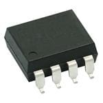
ICGOO电子元器件商城为您提供HCPL-3150-500E由Avago Technologies设计生产,在icgoo商城现货销售,并且可以通过原厂、代理商等渠道进行代购。 HCPL-3150-500E价格参考¥11.78-¥25.41。Avago TechnologiesHCPL-3150-500E封装/规格:隔离器 - 栅极驱动器, 600mA Gate Driver Optical Coupling 3750Vrms 1 Channel 8-DIP Gull Wing。您可以下载HCPL-3150-500E参考资料、Datasheet数据手册功能说明书,资料中有HCPL-3150-500E 详细功能的应用电路图电压和使用方法及教程。
HCPL-3150-500E是Broadcom Limited(现属安华高Avago Technologies)推出的一款高性能光耦隔离栅极驱动器,广泛应用于需要电气隔离和高可靠性的功率电子系统中。其主要应用场景包括:

1. 电机驱动:用于工业变频器、伺服驱动器和无刷直流电机控制中,驱动IGBT或MOSFET功率开关,实现强弱电隔离,提高系统抗干扰能力。

2. 开关电源(SMPS):在大功率AC/DC与DC/DC转换器中,作为半桥或全桥拓扑的栅极驱动器,确保控制电路与高压侧开关之间的安全隔离。

3. 逆变器系统:常见于太阳能光伏逆变器、UPS不间断电源及电动汽车充电桩中,用于驱动高压侧和低压侧的功率器件,保障控制信号的可靠传输。

4. 工业自动化与电源管理:适用于PLC模块、工业电源模块等对噪声抑制和系统稳定性要求较高的场合。

该器件具备高共模瞬态抑制能力(CMTI)、快速传播延迟和宽工作温度范围,支持最高达1.5A的峰值输出电流,适合高温、高噪声的工业环境。同时采用紧凑的SO-8封装,便于PCB布局和散热设计。整体上,HCPL-3150-500E是一款兼顾性能与可靠性的隔离驱动解决方案,特别适用于中高功率开关系统的安全驱动需求。
| 参数 | 数值 |
| 产品目录 | |
| 描述 | OPTOCOUPLER GATE DRIVE 0.6A 8SMD逻辑输出光电耦合器 0.5A IGBT Gate Drive |
| 产品分类 | |
| 品牌 | Avago Technologies US Inc. |
| 产品手册 | |
| 产品图片 |
|
| rohs | 符合RoHS无铅 / 符合限制有害物质指令(RoHS)规范要求 |
| 产品系列 | 光耦合器/光电耦合器,逻辑输出光电耦合器,Avago Technologies HCPL-3150-500E- |
| 数据手册 | http://www.avagotech.com/docs/AV02-0164EN |
| 产品型号 | HCPL-3150-500E |
| PCN封装 | |
| 上升/下降时间(典型值) | 100ns, 100ns |
| 不同If时的传播延迟高-低 | 300ns @ 7mA ~ 16mA |
| 产品目录绘图 |
|
| 产品种类 | 逻辑输出光电耦合器 |
| 传播延迟tpLH/tpHL(最大值) | 500ns, 500ns |
| 供应商器件封装 | 8-DIP 鸥翼型 |
| 共模瞬态抗扰度(最小值) | 15kV/µs |
| 其它名称 | 516-1584-2 |
| 包装 | 带卷 (TR) |
| 商标 | Avago Technologies |
| 安装类型 | 表面贴装 |
| 封装 | Reel |
| 封装/外壳 | 8-SMD,鸥翼型 |
| 封装/箱体 | DIP-8 Gull Wing |
| 工作温度 | -40°C ~ 100°C |
| 工厂包装数量 | 1000 |
| 技术 | 光学耦合 |
| 数据速率 | - |
| 最大传播延迟时间 | 500 ns |
| 最大功率耗散 | 295 mW |
| 最大反向二极管电压 | 5 V |
| 最大工作温度 | + 100 C |
| 最大正向二极管电压 | 1.8 V |
| 最大正向二极管电流 | 16 mA |
| 最小工作温度 | - 40 C |
| 最小正向二极管电压 | 1.2 V |
| 标准包装 | 1,000 |
| 每芯片的通道数量 | 1 Channel |
| 电压-正向(Vf)(典型值) | 1.5V |
| 电压-电源 | 15 V ~ 30 V |
| 电压-隔离 | 3750Vrms |
| 电流-DC正向(If) | 25mA |
| 电流-峰值输出 | 600mA |
| 电流-输出/通道 | 600mA |
| 电流-输出高,低 | 500mA, 500mA |
| 绝缘电压 | 3750 Vrms |
| 脉宽失真(最大) | 300ns |
| 认可 | UR |
| 输入类型 | DC |
| 输出类型 | Open Collector |
| 通道数 | 1 |


- 商务部:美国ITC正式对集成电路等产品启动337调查
- 曝三星4nm工艺存在良率问题 高通将骁龙8 Gen1或转产台积电
- 太阳诱电将投资9.5亿元在常州建新厂生产MLCC 预计2023年完工
- 英特尔发布欧洲新工厂建设计划 深化IDM 2.0 战略
- 台积电先进制程称霸业界 有大客户加持明年业绩稳了
- 达到5530亿美元!SIA预计今年全球半导体销售额将创下新高
- 英特尔拟将自动驾驶子公司Mobileye上市 估值或超500亿美元
- 三星加码芯片和SET,合并消费电子和移动部门,撤换高东真等 CEO
- 三星电子宣布重大人事变动 还合并消费电子和移动部门
- 海关总署:前11个月进口集成电路产品价值2.52万亿元 增长14.8%


.jpg)
PDF Datasheet 数据手册内容提取
Data Sheet HCPL-3150 (Single Channel), HCPL-315J (Dual Channel) 0.5 Amp Output Current IGBT Gate Drive Optocoupler Overview Features The Broadcom® HCPL-315X consists of an LED optically 0.6A maximum peak output current coupled to an integrated circuit with a power output stage. 0.5A minimum peak output current This optocoupler is ideally suited for driving power IGBTs 15-kV/µs minimum Common Mode Rejection (CMR) at and MOSFETs used in motor control inverter applications. V = 1500V CM The high operating voltage range of the output stage 1.0V maximum low level output voltage (VOL) provides the drive voltages required by gate-controlled eliminates need for negative gate drive devices. The voltage and current supplied by this ICC = 5 mA maximum supply current optocoupler makes it ideally suited for directly driving IGBTs Under voltage lock-out protection (UVLO) with with ratings up to 1200V/50A. For IGBTs with higher ratings, hysteresis the HCPL-3150/315J can be used to drive a discrete power Wide operating VCC range: 15V to 30V stage which drives the IGBT gate. 0.5-µs maximum propagation delay ±0.35-µs maximum delay between devices/channels Applications Industrial temperature range: –40°C to 100°C Isolated IGBT/MOSFET gate drive HCPL-315J: channel one to channel two output isolation = 1500 Vrms/1 min. AC and brushless DC motor drives Safety and regulatory approval: Industrial inverters – UL recognized (UL1577), Switch mode power supplies (SMPSs) 3750 Vrms/1 min. (HCPL-3150) Uninterruptable power supplies (UPSs) 5000 Vrms/1 min. (HCPL-315J) – IEC/EN/DIN EN 60747-5-5 approved V = 630 V (HCPL-3150 option 060 only) IORM peak V = 1414 V (HCPL-315J) CSA certified IORM peak CAUTION! It is advised that normal static precautions be taken in handling and assembly of this component to prevent damage and/or degradation that may be induced by ESD. The components featured in this data sheet are not to be used in military or aerospace applications or environments. Broadcom AV02-0164EN October 20, 2017
HCPL-3150 (Single Channel), HCPL-315J (Dual Channel) Data Sheet 0.5 Amp Output Current IGBT Gate Drive Optocoupler Functional Diagram N/C 1 16 VCC N/C 1 8 VCC ANODE 2 15 VO TRUTH TABLE CATHODE 3 14 VEE VCC – VEE VCC – VEE ANODE 2 7 VO SHIELD LED P(Oi.SeI.T TIUVER-NG-OOINN)G N(Ei.GeA. TTUIVREN-G-OOFIFN)G VO OFF 0 - 30 V 0 - 30 V LOW CATHODE 3 6 VO ANODE 6 11 VCC ON 0 - 11 V 0 - 9.5 V LOW CATHODE 7 10 VO ON 11 - 13.5 V 9.5 - 12 V TRANSITION N/C 4 5 VEE ON 13.5 - 30 V 12 - 30 V HIGH SHIELD N/C 8 9 VEE SHIELD HCPL-3150 HCPL-315J NOTE: A 0.1-µF bypass capacitor must be connected between the V and V pins for each channel. CC EE Selection Guide: Inverter Gate Drive Optoisolators Widebody Package Type 8-Pin DIP (300 mil) (400 mil) Small Outline SO-16 Part Number HCPL-3150 HCPL-3120 HCPL-J312 HCPL-J314 HCNW- HCPL-315J HCPL-316J HCPL-314J 3120 Number of Channels 1 1 1 1 1 2 1 2 IEC/EN/DIN V V V V IORM IORM IORM IORM EN 60747-5-5 Approvals 630 Vpeak 1230 Vpeak 1414 Vpeak 1414 Vpeak Option 060 UL Approval 5000 Vrms/1 min. 5000 Vrms/1min. 5000 Vrms/ 5000 Vrms/1 min. 1 min. Output Peak Current 0.5A 2A 2A 0.4A 2A 0.5A 2A 0.4A CMR (Minimum) 15 kV/µs 10 kV/µs 15 kV/µs 10 kV/µs UVLO Yes No Yes No Fault Status No Yes No Broadcom AV02-0164EN 2
HCPL-3150 (Single Channel), HCPL-315J (Dual Channel) Data Sheet 0.5 Amp Output Current IGBT Gate Drive Optocoupler Ordering Information HCPL-3150 is UL Recognized with 3750 Vrms for 1 minute per UL1577. HCPL-315J is UL Recognized with 5000 Vrms for 1 minute per UL1577. Option RoHS Non RoHS Surface IEC/EN/DIN Part Number Compliant Compliant Package Mount Gull Wing Tape & Reel EN 60747-5-5 Quantity HCPL-3150 -000E No option 300 mil 50 per tube -300E #300 DIP-8 X X 50 per tube -500E #500 X X X 1000 per reel -060E #060 X 50 per tube -360E #360 X X X 50 per tube -560E #560 X X X X 1000 per reel -560ME No option X X X X 1000 per reel HCPL-315J -000E No option SO-16 X X 45 per tube -500E #500 X X X 850 per reel To order, choose a part number from the part number column and combine with the desired option from the option column to form an order entry. Example 1: HCPL-3150-560E to order product of 300 mil DIP Gull Wing Surface Mount package in Tape and Reel packaging with IEC/EN/DIN EN 60747-5-5 Safety Approval in RoHS compliant. Example 2: HCPL-3150 to order product of 300 mil DIP package in tube packaging and non RoHS compliant. Option data sheets are available. Contact your Broadcom sales representative or authorized distributor for information. NOTE: The notation “#XXX” is used for existing products, while (new) products launched since July 15, 2001 and RoHS compliant option use “-XXXE.” Broadcom AV02-0164EN 3
HCPL-3150 (Single Channel), HCPL-315J (Dual Channel) Data Sheet 0.5 Amp Output Current IGBT Gate Drive Optocoupler Package Outline Drawings Standard DIP Package 9.80 ± 0.25 (0.386 ± 0.010) 7.62 ± 0.25 (0.300 ± 0.010) Device Part Number 8 7 6 5 6.35 ± 0.25 (0.250 ± 0.010) Avago A NNNN Z Test Rating Code • Lead Free YYWW UL Logo EEE P Special Program Code Pin 1 Dot 1 2 3 4 Date Code Lot ID 1.19 (0.047) MAX. 1.78 (0.070) MAX. + 0.076 5 TYP. 0.254 - 0.051 + 0.003) (0.010 - 0.002) 3.56 ± 0.13 4.70 (0.185) MAX. (0.140 ± 0.005) 0.51 (0.020) MIN. 2.92 (0.115) MIN. DIMENSIONS IN MILLIMETERS AND (INCHES). 1.080 ± 0.320 0.65 (0.025) MAX. OPTION NUMBERS 300 AND 500 NOT MARKED. (0.043 ± 0.013) NOTE: FLOATING LEAD PROTRUSION IS 0.25 mm (10 mils) MAX. 2.54 ± 0.25 (0.100 ± 0.010) Broadcom AV02-0164EN 4
HCPL-3150 (Single Channel), HCPL-315J (Dual Channel) Data Sheet 0.5 Amp Output Current IGBT Gate Drive Optocoupler Gull-Wing Surface-Mount Option 300 9.80 ± 0.25 LAND PATTERN RECOMMENDATION (0.386 ± 0.010) 1.016 (0.040) Device Part Number 8 7 6 5 Avago A NNNN Z Test Rating Code • Lead Free YYWW UL Logo (06..235500 ±± 00..02150) 10.9 (0.430) EEE P Special Program Code Pin 1 Dot 1 2 3 4 Date Code Lot ID 2.0 (0.080) 1.27 (0.050) 1.780 9.65 ± 0.25 (0.070) (0.380 ± 0.010) 1.19 MAX. 7.62 ± 0.25 (0.047) (0.300 ± 0.010) MAX. + 0.076 0.254 - 0.051 3.56 ± 0.13 + 0.003) (0.140 ± 0.005) (0.010 - 0.002) 1.080 ± 0.320 0.635 ± 0.25 (0.043 ± 0.013) (0.025 ± 0.010) 12° NOM. 2.54 0.635 ± 0.130 (0.100) (0.025 ± 0.005) BSC DIMENSIONS IN MILLIMETERS (INCHES). LEAD COPLANARITY = 0.10 mm (0.004 INCHES). NOTE: FLOATING LEAD PROTRUSION IS 0.5 mm (20 mils) MAX. Broadcom AV02-0164EN 5
HCPL-3150 (Single Channel), HCPL-315J (Dual Channel) Data Sheet 0.5 Amp Output Current IGBT Gate Drive Optocoupler 16-Lead Surface Mount Package 0.457 LAND PATTERN RECOMMENDATION 1.270 (0.018) (0.050) 0.64 (0.025) 16 15 14 11 10 9 TYPE NUMBER DATE CODE A XXXX AVAGO LEAD-FREE YYWW 7.493 ± 0.254 11.63 (0.458) EEE (0.295 ± 0.010) PIN 1 DOT LOT ID 2.16 (0.085) 1 2 3 6 7 8 10.312 ± 0.254 (0.406 ± 0.10) 8.763 ± 0.254 ALL LEADS TO 9° (0.345 ± 0.010) BE COPLANAR ± 0.05 (0.002) 3.505 ± 0.127 0.457 0-8° 0.203 ± 0.076 (0.138 ± 0.005) (0.018) 0.64 (0.025) MIN. (0.008 ± 0.003) STANDOFF 10.363 ± 0.254 Dimensions in Millimeters (Inches) (0.408 ± 0.010) Floating lead protrusion is 0.25 mm (10 mils) Max. Note: Initial and continued variation in color of the white mold compound is normal and does not affect performance or reliability of the device Recommended Pb-Free IR Profile Recommended reflow condition as per JEDEC Standard, J-STD-020 (latest revision). Non-halide flux should be used. Regulatory Information The HCPL-3150 and HCPL-315J have been approved by the following organizations. UL Recognized under UL 1577, Component Recognition Program, File E55361. CSA Approved under CSA Component Acceptance Notice #5, File CA 88324. IEC/EN/DIN EN 60747-5-5 Approved under: DIN EN 60747-5-5(VDE 0884-5):2011-11 (Option 060 and HCPL-315J only) Broadcom AV02-0164EN 6
HCPL-3150 (Single Channel), HCPL-315J (Dual Channel) Data Sheet 0.5 Amp Output Current IGBT Gate Drive Optocoupler IEC/EN/DIN EN 60747-5-5 Insulation Characteristics Description Symbol HCPL-3150#060 HCPL-315J Units Installation classification per DIN VDE 0110/1.89, Table 1 For rated mains voltage ≤ 150 Vrms I - IV For rated mains voltage ≤ 300 Vrms I - IV I - IV For rated mains voltage ≤ 600 Vrms I - III I - IV For rated mains voltage ≤ 1000 Vrms I - II I-III Climatic Classification 55/100/21 55/100/21 Pollution Degree (DIN VDE 0110/1.89) 2 2 Maximum Working Insulation Voltage V 630 1414 Vpeak IORM Input to Output Test Voltage, Method ba VPR 1181 2652 Vpeak V × 1.875 = V , 100% Production Test with t =1 second, IORM PR m Partial discharge < 5 pC Input to Output Test Voltage, Method aa VPR 945 2262 Vpeak V × 1.6 = V , Type and Sample Test, t = 10 seconds, IORM PR m Partial discharge < 5 pC Highest Allowable Overvoltagea VIOTM 6000 8000 Vpeak (Transient Overvoltage t = 60 seconds) ini Safety-Limiting Values – Maximum Values Allowed in the Event of a Failure, Also See Figure41 and Figure42. Case Temperature TS 175 175 °C Input Current I 230 400 mA S, INPUT Output Power P 600 1200 mW S, OUTPUT Insulation Resistance at TS, VIO = 500V RS ≥ 109 ≥ 109 Ω a. Refer to IEC/EN/DIN EN 60747-5-5 Optoisolator Safety Standard section of the Broadcom Regulatory Guide to Isolation Circuits, AV02-2041EN for a detailed description of Method a and Method b partial discharge test profiles. NOTE: Isolation characteristics are guaranteed only within the safety maximum ratings that must be ensured by protective circuits in application. Broadcom AV02-0164EN 7
HCPL-3150 (Single Channel), HCPL-315J (Dual Channel) Data Sheet 0.5 Amp Output Current IGBT Gate Drive Optocoupler Insulation and Safety Related Specifications Parameter Symbol HCPL-3150 HCPL-315J Units Conditions Minimum External Air Gap L(101) 7.1 8.3 mm Measured from input terminals to output (External Clearance terminals, shortest distance through air. Minimum External Tracking L(102) 7.4 8.3 mm Measured from input terminals to output (External Creepage) terminals, shortest distance path along body. Minimum Internal Plastic Gap 0.08 ≥ 0.5 mm Through insulation distance conductor to (Internal Clearance) conductor. Tracking Resistance (Comparative CTI ≥ 175 ≥ 175 Volts DIN IEC 112/VDE 0303 Part 1 Tracking Index) Isolation Group IIIa IIIa Material Group (DIN VDE 0110, 1/89, Table1) Option 300 – surface mount classification is Class A in accordance with CECC 00802. Absolute Maximum Ratings Parameter Symbol Min. Max. Units Note Storage Temperature T –55 125 °C S Operating Temperature T –40 100 °C A Average Input Current IF(AVG) — 25 mA a, b Peak Transient Input Current (<1-µs pulse width, 300 pps) I — 1.0 A F(TRAN) Reverse Input Voltage V — 5 Volts R “High” Peak Output Current IOH(PEAK) — 0.6 A b, c “Low” Peak Output Current IOL(PEAK) — 0.6 A b, c Supply Voltage (V – V ) 0 35 Volts CC EE Output Voltage V 0 V Volts O(PEAK) CC Output Power Dissipation PO — 250 mW b, d Total Power Dissipation PT — 295 mW b, e Lead Solder Temperature 260°C for 10 seconds, 1.6 mm below seating plane Solder Reflow Temperature Profile See Package Outline Drawings Section a. Derate linearly above 70°C free-air temperature at a rate of 0.3 mA/°C. b. Each channel. c. Maximum pulse width = 10 µs, maximum duty cycle = 0.2%. This value is intended to allow for component tolerances for designs with I peak O minimum = 0.5A. See the Applications section for additional details on limiting I H peak. O d. Derate linearly above 70°C free-air temperature at a rate of 4.8 mW/°C. e. Derate linearly above 70°C free-air temperature at a rate of 5.4 mW/°C. The maximum LED junction temperature should not exceed 125°C. Broadcom AV02-0164EN 8
HCPL-3150 (Single Channel), HCPL-315J (Dual Channel) Data Sheet 0.5 Amp Output Current IGBT Gate Drive Optocoupler Recommended Operating Conditions Parameter Symbol Min. Max. Units Power Supply Voltage (V – V ) 15 30 V CC EE Input Current (ON) I 7 16 mA F(ON) Input Voltage (OFF) V –3.6 0.8 V F(OFF) Operating Temperature T –40 100 °C A Broadcom AV02-0164EN 9
HCPL-3150 (Single Channel), HCPL-315J (Dual Channel) Data Sheet 0.5 Amp Output Current IGBT Gate Drive Optocoupler Electrical Specifications (DC) Over recommended operating conditions (T = –40°C to 100°C, I = 7 mA to 16 mA, V = –3.6V to 0.8V, V =15V A F(ON) F(OFF) CC to 30V, V = Ground, each channel) unless otherwise specified. EE Parameter Symbol Min. Typ.a Max. Units Test Conditions Figure Note High Level Output Current I 0.1 0.4 — A V = (V – 4V) 2, 3, 5 OH O CC 0.5 — — V = (V – 15V) 17 b O CC Low Level Output Current I 0.1 0.6 — A V = (V + 2.5V) 5, 6 c OL O EE 0.5 — — V = (V + 15V) 18 b O EE High Level Output Voltage VOH (VCC – 4) (VCC – 3) — V IO = –100 mA 1, 3, 19 d, e Low Level Output Voltage V — 0.4 1.0 V I = 100 mA 4, 6, 20 OL O High Level Supply Current I — 2.5 5.0 mA Output Open, I = 7 to 16 mA 7, 8 f CCH F Low Level Supply Current I — 2.7 5.0 mA Output Open, CCL V = –3.0 to +0.8V F Threshold Input Current Low to I — 2.2 5.0 mA HCPL-3150 I = 0 mA, 9, 15, FLH O High — 2.6 6.4 HCPL-315J V > 5V 21 O Threshold Input Voltage High V 0.8 — — V FHL to Low Input Forward Voltage V 1.2 1.5 1.8 V HCPL-3150 I = 10 mA 16 F F 1.6 1.95 HCPL-315J Temperature Coefficient of ΔV /ΔT — –1.6 — mV/°C I = 10 mA F A F Forward Voltage Input Reverse Breakdown BV 5 — — V HCPL-3150 I = 10 µA R R Voltage 3 HCPL-315J I = 10 µA R Input Capacitance C — 70 — pF f = 1 MHz, V = 0V IN F UVLO Threshold V 11.0 12.3 13.5 V V > 5 V 22, 40 UVLO+ O V 9.5 10.7 12.0 I = 10 mA UVLO- F UVLO Hysteresis UVLO — 1.6 — V HYS a. All typical values at T = 25°C and V – V = 30V, unless otherwise noted. A CC EE b. Maximum pulse width = 10 µs, maximum duty cycle = 0.2%. This value is intended to allow for component tolerances for designs with I peak O minimum = 0.5 A. See Applications section for additional details on limiting I peak. OH c. Maximum pulse width = 50 µs, maximum duty cycle = 0.5%. d. In this test, V is measured with a dc load current. When driving capacitive loads V will approach V as I approaches zero amps. OH OH CC OH e. Maximum pulse width = 1 ms, maximum duty cycle = 20%. f. Each channel. Broadcom AV02-0164EN 10
HCPL-3150 (Single Channel), HCPL-315J (Dual Channel) Data Sheet 0.5 Amp Output Current IGBT Gate Drive Optocoupler Switching Specifications (AC) Over recommended operating conditions (T = –40 to 100°C, I = 7 mA to 16 mA, V = –3.6V to 0.8V, V = 15V A F(ON) F(OFF) CC to 30V, V = Ground, each channel) unless otherwise specified. EE Parameter Symbol Min. Typ.a Max. Units Test Conditions Figure Note Propagation Delay Time to High t 0.10 0.30 0.50 µs Rg = 47 Ω, Cg = 3 nF, 10, 11, b PLH Output Level f = 10 kHz, Duty Cycle = 50% 12, 13, Propagation Delay Time to Low t 0.10 0.3 0.50 µs 14, 23 PHL Output Level Pulse Width Distortion PWD 0.3 µs c Propagation Delay Difference PDD –0.35 — 0.35 µs 38, 39 d Between Any Two Parts or (t – t ) PHL PLH Channels Rise Time t — 0.1 — µs 23 r Fall Time t — 0.1 — µs f UVLO Turn On Delay t — 0.8 — µs V > 5V, I = 10 mA 22 UVLO ON O F UVLO Turn Off Delay t — 0.6 — µs V < 5V, I = 10 mA UVLO OFF O F Output High Level Common Mode |CMH| 15 30 — kV/µs TA = 25°C, IF = 10 to 16 mA, 24 e, f Transient Immunity V = 1500V, V = 30 V CM CC Output Low Level Common Mode |CML| 15 30 — kV/µs TA = 25°C, VCM = 1500V, e, g Transient Immunity V = 0 V, V = 30V F CC a. All typical values at T = 25°C and V – V = 30V, unless otherwise noted. A CC EE b. This load condition approximates the gate load of a 1200 V/25 A IGBT c. Pulse Width Distortion (PWD) is defined as |t – t | for any given device. PHL PLH d. The difference between t and t between any two parts or channels under the same test condition. PHL PLH e. Pins 1 and 4 (HCPL-3150) and pins 3 and 4 (HCPL-315J) need to be connected to LED common. f. Common mode transient immunity in the high state is the maximum tolerable |dV /dt| of the common mode pulse, V , to assure that the CM CM output will remain in the high state (that is, V > 15.0V). O g. Common mode transient immunity in a low state is the maximum tolerable |dV /dt| of the common mode pulse, V , to assure that the CM CM output will remain in a low state (that is, V < 1.0V). O Broadcom AV02-0164EN 11
HCPL-3150 (Single Channel), HCPL-315J (Dual Channel) Data Sheet 0.5 Amp Output Current IGBT Gate Drive Optocoupler Package Characteristics Each channel, unless otherwise specified. Parameter Symbol Device Min. Typ.a Max. Units Test Conditions Figure Note Input-Output Momentary VISO HCPL-3150 3750 — — Vrms RH < 50%, t = 1 min., c, d Withstand Voltageb HCPL-315J 5000 TA = 25°C Output-Output Momentary V HCPL-315J 1500 — — Vrms RH < 50%, t = 1 min., e O-O Withstand Voltageb TA = 25°C Resistance (Input-Output) RI-O — 1012 — Ω VI-O = 500 VDC f Capacitance (Input-Output) C HCPL-3150 — 0.6 — pF f = 1 MHz I-O HCPL-315J 1.3 LED-to-Case Thermal θ HCPL-3150 — 391 — °C/W Thermocouple 29, 30 g LC Resistance located at center LED-to-Detector Thermal θ HCPL-3150 — 439 — °C/W underside of package LD Resistance Detector-to-Case Thermal θ HCPL-3150 — 119 — °C/W DC Resistance a. All typical values at T = 25°C and V – V = 30V, unless otherwise noted. A CC EE b. The Input-Output/Output-Output Momentary Withstand Voltage is a dielectric voltage rating that should not be interpreted as an input-output/ output-output continuous voltage rating. For the continuous voltage rating, refer to your equipment level safety specification or Broadcom Application Note 1074, Optocoupler Input-Output Endurance Voltage. c. In accordance with UL1577, each HCPL-3150 optocoupler is proof tested by applying an insulation test voltage ≥ 4500 Vrms (≥ 6000 Vrms for the HCPL-315J) for 1 second. This test is performed before the 100% production test for partial discharge (method b) shown in the IEC/ EN/DIN EN 60747-5-5 Insulation Characteristics Table, if applicable. d. Device considered a two-terminal device: pins on input side shorted together and pins on output side shorted together. e. Device considered a two terminal device: Channel one output side pins shorted together, and channel two output side pins shorted together. f. Device considered a two-terminal device: pins on input side shorted together and pins on output side shorted together. g. See the thermal model for the HCPL-315J in the application section of this data sheet. Broadcom AV02-0164EN 12
HCPL-3150 (Single Channel), HCPL-315J (Dual Channel) Data Sheet 0.5 Amp Output Current IGBT Gate Drive Optocoupler Figure 1: V vs. Temperature Figure 2: I vs. Temperature Figure 3: V vs. I OH OH OH OH 0 0.50 -1 IF = 7 to 16 mA IF = 7 to 16 mA - V) – HIGH OUTPUT VOLTAGE DROP – VHCC ---123 VIVOCEUECT == = 01 - 5V1 t0o0 3m0A V I – OUTPUT HIGH CURRENT – AOH 0000....44335050 VVVOCEECU ==T = 01 5 VV tCoC 3- 04 VV - V) – OUTPUT HIGH VOLTAGE DROP – VHCC ----2354 IVVFCE =EC == 7 01to 5V 1to6 3m0A V 12-40500 ° ° C°CC (VO (VO -4 0.25 -6 -40 -20 0 20 40 60 80 100 -40 -20 0 20 40 60 80 100 0 0.2 0.4 0.6 0.8 1.0 TA – TEMPERATURE – °C TA – TEMPERATURE – °C IOH – OUTPUT HIGH CURRENT – A Figure 4: V vs. Temperature Figure 5: I vs. Temperature Figure 6: V vs. I OL OL OL OL 1.0 1.0 5 VF(OFF) = -3.0 to 0.8 V VF(OFF) = -3.0 to 0.8 V IOUT = 100 mA VCC = 15 to 30 V V – OUTPUT LOW VOLTAGE – VOL 0000....8624 VVCEEC == 01 5V to 30 V I – OUTPUT LOW CURRENT – AOL 0000....8426 VVVFOC(CUO =TF F= 1) 5=2 .t 5-o3 V3.00 tVo 0.8 V V – OUTPUT LOW VOLTAGE – VOL 2413 VEE = 0 V 100 °C VEE = 0 V 25 °C -40 °C 0 0 0 -40 -20 0 20 40 60 80 100 -40 -20 0 20 40 60 80 100 0 0.2 0.4 0.6 0.8 1.0 TA – TEMPERATURE – °C TA – TEMPERATURE – °C IOL – OUTPUT LOW CURRENT – A Figure 7: I vs. Temperature Figure 8: I vs. V Figure 9: I vs. Temperature CC CC CC FLH 3.5 3.5 5 IICCCCHL IICCCCHL D – mA 4 VVOCEUECT ==PU 01T 5V = T OO P30EN V I – SUPPLY CURRENT – mACC 322...050 VVIIFFCE ==EC == 10 0 03m 0mVA VA f ofor rIC ICCLCH I – SUPPLY CURRENT – mACC 322...050 VITIFFAE == E= = 10 2 0 0m5 m V°ACA f ofor rIC ICCLCH – LOW TO HIGH CURRENT THRESHOLH 321 1.5 1.5 IFL 0 -40 -20 0 20 40 60 80 100 15 20 25 30 -40 -20 0 20 40 60 80 100 TA – TEMPERATURE – °C VCC – SUPPLY VOLTAGE – V TA – TEMPERATURE – °C Broadcom AV02-0164EN 13
HCPL-3150 (Single Channel), HCPL-315J (Dual Channel) Data Sheet 0.5 Amp Output Current IGBT Gate Drive Optocoupler Figure 10: Propagation Delay vs. V Figure 11: Propagation Delay vs. I Figure 12: Propagation Delay vs. CC F Temperature 500 500 500 RITFAg = == 1 24057 m °(cid:58)CA TTPPLHHL VRTACg C == = 24 3570 °(cid:58) CV,, VCEgE = = 3 0 n VF VIIFFC((COO NF=F) )3= =0 1 V00, m mVEAAE = 0 V DELAY – ns 400 CDf g=U T= 1Y 03 C kYnHCFLzE = 50% DELAY – ns 400 Df =UT 1Y0 C kYHCLzE = 50% DELAY – ns 400 RDf =gU T =1Y0 4C k7YH C(cid:58)LzE, C=g 5 =0 %3 nF N N N O 300 O 300 O 300 GATI GATI GATI OPA OPA OPA R R R – P 200 – P 200 – P 200 Tp Tp Tp TPLH TPLH TPHL TPHL 100 100 100 15 20 25 30 6 8 10 12 14 16 -40 -20 0 20 40 60 80 100 VCC – SUPPLY VOLTAGE – V IF – FORWARD LED CURRENT – mA TA – TEMPERATURE – °C Figure 13: Propagation Delay vs. Rg Figure 14: Propagation Delay vs. Cg Figure 15: Transfer Characteristics 500 500 30 VCC = 30 V, VEE = 0 V VCC = 30 V, VEE = 0 V ITFA = = 1 205 m °CA ITFA = = 1 205 m °CA 25 T– PROPAGATION DELAY – nsp 432000000 CDf g=U T= 1Y 03 C kYnHCFLzE = 50% TPLH T– PROPAGATION DELAY – nsp 432000000 RDf =gU T =1Y0 4C k7YH C(cid:58)LzE = 50% TPLH V– OUTPUT VOLTAGE – VO 1215500 TPHL TPHL 100 100 0 0 50 100 150 200 0 20 40 60 80 100 0 1 2 3 4 5 Rg – SERIES LOAD RESISTANCE – (cid:58) Cg – LOAD CAPACITANCE – nF IF – FORWARD LED CURRENT – mA Figure 16: Input Current vs. Forward Voltage 1000 TA = 25°C 100 A IF m NT – 10 VF+ RE – R D CU 1.0 R A W OR 0.1 – F I F 0.01 0.001 1.10 1.20 1.30 1.40 1.50 1.60 VF – FORWARD VOLTAGE – V Broadcom AV02-0164EN 14
HCPL-3150 (Single Channel), HCPL-315J (Dual Channel) Data Sheet 0.5 Amp Output Current IGBT Gate Drive Optocoupler Figure 17: I Test Circuit Figure 18: I Test Circuit OH OL 1 8 1 8 0.1 μF 0.1 μF IOL 2 7 +– 4 V 2 7 IF = 7 to + VCC = 15 +– VtCoC 3=0 1V5 16 mA – to 30 V 3 6 3 6 2.5 V +– IOH 4 5 4 5 Figure 19: V Test Circuit Figure 20: V Test Circuit OH OL 1 8 1 8 0.1 μF 0.1 μF 100 mA 2 7 VOH 2 7 IF1 =6 m7 Ato +– VtCoC 3=0 1V5 +– VtCoC 3=0 1V5 3 6 3 6 VOL 100 mA 4 5 4 5 Figure 21: I Test Circuit Figure 22: UVLO Test Circuit FLH 1 8 1 8 0.1 μF 0.1 μF 2 7 2 7 IF VO > 5 V +– VtCoC 3=0 1V5 IF = 10 mA VO > 5 V +– VCC 3 6 3 6 4 5 4 5 Broadcom AV02-0164EN 15
HCPL-3150 (Single Channel), HCPL-315J (Dual Channel) Data Sheet 0.5 Amp Output Current IGBT Gate Drive Optocoupler Figure 23: t , t , t, and t Test Circuit and Waveforms PLH PHL r f 1 8 IF = 7 t5o0 106 (cid:58) mA 2 7 0.1 μF +– VtCoC 3=0 1V5 IF tr tf 10 KHz +– VO 90% 50% DUTY 3 6 47 (cid:58) CYCLE 50% 3 nF VOUT 10% 4 5 tPLH tPHL Figure 24: CMR Test Circuit and Waveforms VCM (cid:71)V VCM 1 8 = IF 0.1 μF (cid:71)t (cid:39)t A 0 V 2 7 B 5 V +– VO +– (cid:39)t 3 6 VCC = 30 V VO VOH SWITCH AT A: IF = 10 mA 4 5 VO VOL SWITCH AT B: IF = 0 mA +– VCM = 1500 V Applications Information Eliminating Negative IGBT Gate Drive To keep the IGBT firmly off, the HCPL-3150/315J has a very low maximum V specification of 1.0V. The HCPL-3150/315J OL realizes this very low V by using a DMOS transistor with 4Ω (typical) on resistance in its pull-down circuit. When the OL HCPL3150/315J is in the low state, the IGBT gate is shorted to the emitter by Rg + 4Ω. Minimizing Rg and the lead inductance from the HCPL-3150/315J to the IGBT gate and emitter (possibly by mounting the HCPL-3150/315J on a small PC board directly above the IGBT) can eliminate the need for negative IGBT gate drive in many applications as shown in Figure25 and Figure26. Care should be taken with such a PC board design to avoid routing the IGBT collector or emitter traces close to the HCPL-3150/315J input as this can result in unwanted coupling of transient signals into the HCPL-3150/ 315J and degrade performance. (If the IGBT drain must be routed near the HCPL-3150/315J input, then the LED should be reverse-biased when in the off state, to prevent the transient signals coupled from the IGBT drain from turning on the HCPL- 3150/315J.) Broadcom AV02-0164EN 16
HCPL-3150 (Single Channel), HCPL-315J (Dual Channel) Data Sheet 0.5 Amp Output Current IGBT Gate Drive Optocoupler Figure 25: Recommended LED Drive and Application Circuit HCPL-3150 +5 V 1 8 VCC = 18 V + HVDC 270 (cid:58) 0.1 μF + – 2 7 Rg CONTROL Q1 3-PHASE INPUT 3 6 AC 74XXX OPEN 4 5 COLLECTOR Q2 - HVDC Figure 26: Recommended LED Drive and Application Circuit (HCPL-315J) + HVDC HCPL-315J +5 V FLOATING 1 16 SUPPLY 270 (cid:58) VCC = 18 V CONTROL 0.1 μF + INPUT – 2 15 74XX Rg OPEN COLLECTOR 3 14 GND 1 3-PHASE AC +5 V 6 11 VCC = 18 V 270 (cid:58) 0.1 μF + – CONTROL INPUT 7 10 Rg 74XX OPEN 8 9 COLLECTOR GND 1 - HVDC Broadcom AV02-0164EN 17
HCPL-3150 (Single Channel), HCPL-315J (Dual Channel) Data Sheet 0.5 Amp Output Current IGBT Gate Drive Optocoupler Selecting the Gate Resistor (Rg) to Minimize IGBT Switching Losses Step 1: Calculate Rg Minimum From the IOL Peak Step 2: Check the HCPL-3150/315J Power Dissipation Specification. The IGBT and Rg in Figure27 and Figure28 and Increase Rg if Necessary. The HCPL-3150/315J total can be analyzed as a simple RC circuit with a voltage power dissipation (P ) is equal to the sum of the emitter T supplied by the HCPL-3150/315J. power (P ) and the output power (P ): E O R g ≥ (VCC – VEE - VOL) PT = PE + PO I OLPEAK P = I (cid:120)V(cid:120)Duty Cycle E F F (V – V - 1.7 V) = CC EE P = P + P I O O(BIAS) O (SWITCHING) OLPEAK = I (cid:120)(V - V ) + E (R , Q )(cid:120)f CC CC EE SW G G (15 V + 5 V - 1.7 V) = 0.6 A For the circuit in Figure27 and Figure28 with I (worst F = 30.5 Ω case) = 16 mA, Rg= 30.5Ω, Max Duty Cycle = 80%, Qg=500 nC, f=20kHz, and T max = 90°C: A The V value of 2V in the previous equation is a OL conservative value of V at the peak current of 0.6A (see P = 16 mA(cid:120)1.8 V(cid:120)0.8 = 23 mW OL E Figure6). At lower Rg values the voltage supplied by the P = 4.25 mA(cid:120)20 V + 4.0 μJ(cid:120)20 kHz HCPL-3150/315J is not an ideal voltage step. This results in O lower peak currents (more margin) than predicted by this = 85 mW + 80 mW analysis. When negative gate drive is not used V in the EE = 165 mW > 154 mW (P @ 90°C previous equation is equal to zero volts. O(MAX) = 250 mW(cid:16)20C(cid:120)4.8 mW/C) Figure 27: HCPL-3150 Typical Application Circuit with Negative IGBT Gate Drive HCPL-3150 +5 V 1 8 270 (cid:58) 0.1 μF + VCC = 15 V + HVDC – 2 7 Rg CONTROL Q1 3-PHASE INPUT 3 6 – VEE = -5 V AC + 74XXX OPEN 4 5 COLLECTOR Q2 - HVDC Broadcom AV02-0164EN 18
HCPL-3150 (Single Channel), HCPL-315J (Dual Channel) Data Sheet 0.5 Amp Output Current IGBT Gate Drive Optocoupler Figure 28: HCPL-315J Typical Application Circuit with Negative IGBT Gate Drive +5 V HCPL-315J FLOATING + HVDC 1 16 SUPPLY 270 (cid:58) VCC = 15 V CONTROL 0.1 μF + INPUT –– 2 15 74XX Rg OPEN COLLECTOR 3 14 – + GND 1 VEE = -5 V 3-PHASE AC +5 V 6 11 VCC = 15 V 270 (cid:58) 0.1 μF + CONTROL –– INPUT 7 10 Rg 74XX OPEN COLLECTOR 8 9 +– VCC = -5 V GND 1 - HVDC Table 1: P and P Parameters E O PE Parameter Description PO Parameter Description I LED Current I Supply Current F CC V LED On Voltage V Positive Supply Voltage F CC Duty Cycle Maximum LED Duty Cycle V Negative Supply Voltage EE E (Rg,Qg) Energy Dissipated in the HCPL-3150/315J for each IGBT Switching SW Cycle (see Figure32) f Switching Frequency Broadcom AV02-0164EN 19
HCPL-3150 (Single Channel), HCPL-315J (Dual Channel) Data Sheet 0.5 Amp Output Current IGBT Gate Drive Optocoupler The value of 4.25 mA for I in the previous equation was Thermal Model (HCPL-3150) CC obtained by derating the I max of 5 mA (which occurs at CC –40°C) to I max at 90°C (see Figure7). The steady state thermal model for the HCPL-3150 is CC shown in Figure29. The thermal resistance values given in Since P for this case is greater than P , Rg must be O O(MAX) this model can be used to calculate the temperatures at increased to reduce the HCPL-3150 power dissipation. each node for a given operating condition. As shown by the model, all heat generated flows through θ which raises CA P = P - P the case temperature T accordingly. The value of θ O(SWITCHING MAX) O(MAX) O(BIAS) C CA depends on the conditions of the board design and is, = 154 mW - 85 mW therefore, determined by the designer. The value of θ = CA = 69 mW 83°C/W was obtained from thermal measurements using a 2.5 in. × 2.5 in. PC board, with small traces (no ground P plane), a single HCPL-3150 soldered into the center of the E = O(SWITCHINGMAX) SW(MAX) f board and still air. The absolute maximum power dissipation derating specifications assume a θ value of 83°C/W. 69 mW CA = = 3.45 μJ 20 kHz For Qg = 500 nC, from Table1, a value of E = 3.45 µJ SW gives a Rg = 41Ω. Figure 29: Thermal Model (cid:84)LD = 439°C/W TJE TJD TJE = LED JUNCTION TEMPERATURE T = DETECTOR IC JUNCTION TEMPERATURE JD (cid:84)LC = 391°C/W (cid:84)DC = 119°C/W TC = CASE TEMPERATURE MEASURED AT THE CENTER OF THE PACKAGE BOTTOM T C (cid:3)(cid:84)LC = LED-TO-CASE THERMAL RESISTANCE (cid:3)(cid:84)LD = LED-TO-DETECTOR THERMAL RESISTANCE (cid:84)CA = 83°C/W* (cid:3)(cid:84)DC = DETECTOR-TO-CASE THERMAL RESISTANCE (cid:3)(cid:84)CA = CASE-TO-AMBIENT THERMAL RESISTANCE *(cid:84)CA WILL DEPEND ON THE BOARD DESIGN AND T THE PLACEMENT OF THE PART. A Broadcom AV02-0164EN 20
HCPL-3150 (Single Channel), HCPL-315J (Dual Channel) Data Sheet 0.5 Amp Output Current IGBT Gate Drive Optocoupler From the thermal mode in Figure29, the LED and detector Thermal Model Dual-Channel (SOIC-16) IC junction temperatures can be expressed as: HCPL-315J Optoisolator T = P(cid:120)(cid:3)((cid:84) ||((cid:84) + (cid:84) ) + (cid:84) ) JE E LC LD DC CA Definitions ( (cid:84) (cid:120) (cid:84) ) + P (cid:120) LC D C + (cid:84) + T D (cid:3)(cid:3)(cid:84)LC + (cid:84)DC + (cid:84)LD CA A θ1, θ2, θ3, θ4, θ5, θ6, θ7, θ8, θ9, θ10: Thermal impedances between nodes as shown in Figure30. Ambient ( (cid:84) (cid:120) (cid:84) ) T = P LC D C + (cid:84) Temperature: Measured approximately 1.25 cm above the JD E (cid:3)(cid:84) + (cid:84) + (cid:84) CA LC DC LD optocoupler with no forced air. + P(cid:120)((cid:84) ||((cid:84) + (cid:84) ) + (cid:84) ) + T D DC LD LC CA A Figure 30: Thermal Impedance Model for HCPL-315J Inserting the values for θ and θ shown in Figure29 LED 1 (cid:84)1 LED 2 LC DC gives: (cid:84)2 (cid:84)3 TJE = PE(cid:120)(230°C/W + (cid:84)CA) + PD(cid:120)(49°C/W + (cid:84)CA) + TA (cid:84)4 (cid:84)5 T = P(cid:120)(49°C/W + (cid:84) ) + P(cid:120)(104°C/W + (cid:84) ) + T JD E CA D CA A DETECTOR 1 DETECTOR 2 For example, given PE = 45 mW, PO = 250 mW, TA = 70°C (cid:84)7 (cid:84)10 (cid:84)6 and θ = 83°C/W: (cid:84)8 (cid:84)9 CA T = P(cid:120)313°C/W + P(cid:120)132°C/W + T JE E D A = 45 mW(cid:120)313°C/W + 250 mW (cid:120)132°C/W + 70°C = 117°C T = P(cid:120)132°C/W + P(cid:120)187°C/W + T JD E D A = 45 mW(cid:120)132C/W + 250 mW (cid:120)187°C/W + 70°C = 123°C AMBIENT T and T should be limited to 125°C based on the board Figure 31: Power Dissipation JE JD layout and part placement (θ ) specific to the application. CA PE1 PD1 PE2 PD2 Description This thermal model assumes that a 16-pin dual-channel (SOIC-16) optocoupler is soldered into an 8.5 cm × 8.1 cm printed circuit board (PCB). These optocouplers are hybrid devices with four die: two LEDs and two detectors. The temperature at the LED and the detector of the optocoupler can be calculated by using the equations below. Broadcom AV02-0164EN 21
HCPL-3150 (Single Channel), HCPL-315J (Dual Channel) Data Sheet 0.5 Amp Output Current IGBT Gate Drive Optocoupler (cid:39)T = A P + A P +A P +A P E1A 11 E1 12 E2 13 D1 14 D2 (cid:39)T = A P + A P +A P +A P E2A 21 E1 22 E2 23 D1 24 D2 (cid:39)T = A P + A P +A P +A P D1A 31 E1 32 E2 33 D1 34 D2 (cid:39)T = A P + A P +A P +A P D2A 41 E1 42 E2 43 D1 44 D2 where: ΔT = Temperature difference between ambient and LED 1 E1A ΔT = Temperature difference between ambient and LED 2 E2A ΔT = Temperature difference between ambient and detector 1 D1A ΔT = Temperature difference between ambient and detector 2 D2A P = Power dissipation from LED 1; E1 P = Power dissipation from LED 2; E2 P = Power dissipation from detector 1; D1 P = Power dissipation from detector 2 D2 A thermal coefficient (units in °C/W) is a function of thermal impedances θ through θ . xy 1 10 Table 2: Thermal Coefficient Data (units in °C/W) Part Number A11, A22 A12, A21 A13, A31 A24, A42 A14, A41 A23, A32 A33, A44 A34, A43 HCPL-315J 198 64 62 64 83 90 137 69 NOTE: Maximum junction temperature for above part: 125°C. Broadcom AV02-0164EN 22
HCPL-3150 (Single Channel), HCPL-315J (Dual Channel) Data Sheet 0.5 Amp Output Current IGBT Gate Drive Optocoupler LED Drive Circuit Considerations CMR with the LED Off (CMR ) L for Ultra High CMR Performance A high CMR LED drive circuit must keep the LED off (V ≤ F V ) during common mode transients. For example, F(OFF) Without a detector shield, the dominant cause of during a –dV /dt transient in Figure35, the current flowing CM optocoupler CMR failure is capacitive coupling from the through C also flows through the R and V of the LEDP SAT SAT input side of the optocoupler, through the package, to the logic gate. As long as the low state voltage developed detector IC as shown in Figure33. The HCPL-3150/315J across the logic gate is less than V , the LED will F(OFF) improves CMR performance by using a detector IC with an remain off and no common mode failure will occur. optically transparent Faraday shield, which diverts the capacitively coupled current away from the sensitive IC The open collector drive circuit, shown in Figure36, cannot circuitry. How ever, this shield does not eliminate the keep the LED off during a +dV /dt transient, since all the CM capacitive coupling between the LED and optocoupler pins current flowing through C must be supplied by the LED, LEDN 5 to 8 as shown in Figure34. This capacitive coupling and it is not recommended for applications requiring causes perturbations in the LED current during common ultra-high CMR performance. Figure37 is an alternative L mode transients and becomes the major source of CMR drive circuit which, like the recommended application circuit failures for a shielded optocoupler. The main design (Figure25 and Figure26), does achieve ultra-high CMR objective of a high CMR LED drive circuit becomes keeping performance by shunting the LED in the off state. the LED in the proper state (on or off) during common mode transients. For example, the recommended application Under Voltage Lockout Feature circuit (Figure25 and Figure26), can achieve 15kV/µs CMR while minimizing component complexity. The HCPL-3150/315J contains an under voltage lockout (UVLO) feature that is designed to protect the IGBT under Techniques to keep the LED in the proper state are fault conditions that cause the HCPL-3150/315J supply discussed in the next two sections. voltage (equivalent to the fully-charged IGBT gate voltage) to drop below a level necessary to keep the IGBT in a low CMR with the LED On (CMR ) H resistance state. When the HCPL-3150/315J output is in the high state and the supply voltage drops below the A high CMR LED drive circuit must keep the LED on during HCPL-3150/315J V threshold (9.5 < V < 12.0), UVLO- UVLO- common mode transients. This is achieved by overdriving the optocoupler output will go into the low state with a typical the LED current beyond the input threshold so that it is not delay, UVLO Turn Off Delay, of 0.6 µs. When the pulled below the threshold during a transient. A minimum HCPL-3150/315J output is in the low state and the supply LED current of 10 mA provides adequate margin over the voltage rises above the HCPL-3150/315J V threshold UVLO+ maximum I of 5 mA to achieve 15kV/µs CMR. FLH (11.0 < V < 13.5), the optocoupler will go into the high UVLO+ state (assuming LED is “ON”) with a typical delay, UVLO Figure 32: Energy Dissipated in the HCPL-3150 for Each IGBT TURN On Delay, of 0.8 µs. Switching Cycle. 7 Qg = 100 nC μJ 6 Qg = 250 nC – G CYCLE 5 Qg = 500 nC HIN 4 VCC = 19 V WITC VEE = -9 V R S 3 PE GY NER 2 – E w 1 Es 0 0 20 40 60 80 100 Rg – GATE RESISTANCE – (cid:58) Broadcom AV02-0164EN 23
HCPL-3150 (Single Channel), HCPL-315J (Dual Channel) Data Sheet 0.5 Amp Output Current IGBT Gate Drive Optocoupler IPM Dead Time and Propagation Delay Specifications The HCPL-3150/315J includes a Propagation Delay Delaying the LED signal by the maximum propagation delay Difference (PDD) specification intended to help designers difference ensures that the minimum dead time is zero, but minimize “dead time” in their power inverter designs. Dead it does not tell a designer what the maximum dead time will time is the time period during which both the high and low be. The maximum dead time is equivalent to the difference side power transistors (Q1 and Q2 in Figure38) are off. Any between the maximum and minimum propagation delay overlap in Q1 and Q2 conduction will result in large currents difference specifications as shown in Figure39. The flowing through the power devices from the high- to the low- maximum dead time for the HCPL-3150/315J is 700 ns voltage motor rails. (=350ns – (–350ns)) over an operating temperature range of –40°C to 100°C. To minimize dead time in a given design, the turn on of LED2 should be delayed (relative to the turn off of LED1) so that Note that the propagation delays used to calculate PDD and under worst-case conditions, transistor Q1 has just turned dead time are taken at equal temperatures and test off when transistor Q2 turns on, as shown in Figure38. The conditions since the optocouplers under consideration are amount of delay necessary to achieve this condition is equal typically mounted in close proximity to each other and are to the maximum value of the propagation delay difference switching identical IGBTs. specification, PDD , which is specified to be 350 ns over MAX the operating temperature range of –40°C to 100°C. Figure 33: Optocoupler Input to Output Capacitance Model Figure 34: Optocoupler Input to Output Capacitance Model for Unshielded Optocouplers for Shielded Optocouplers 1 8 1 CLEDO1 8 CLEDP CLEDP 2 7 2 7 CLEDO2 3 6 3 6 CLEDN CLEDN 4 5 4 5 SHIELD Figure 35: Equivalent Circuit for Figure 25 During Common Mode Transient +5 V 1 8 0.1 2 CLEDP 7 μF +– VCC = 18 V + VSAT ILEDP – 3 6 • • • CLEDN Rg 4 5 • • • SHIELD * THE ARROWS INDICATE THE DIRECTION OF CURRENT FLOW DURING –dVCM/dt. + – Broadcom AV02-0164EN 24
HCPL-3150 (Single Channel), HCPL-315J (Dual Channel) Data Sheet 0.5 Amp Output Current IGBT Gate Drive Optocoupler Figure 36: Not Recommended Open Collector Drive Circuit Figure 37: Recommended LED Drive Circuit for Ultra-High CMR 1 8 1 8 +5 V +5 V CLEDP CLEDP 2 7 2 7 3 6 3 6 Q1 CLEDN CLEDN ILEDN 4 5 4 5 SHIELD SHIELD Figure 38: Minimum LED Skew for Zero Dead Time Figure 39: Waveforms for Dead Time ILED1 ILED1 VOUT1 VOUT1 Q1 ON Q1 ON Q1 OFF Q1 OFF Q2 ON Q2 ON VOUT2 Q2 OFF VOUT2 Q2 OFF ILED2 ILED2 tPHL MAX tPHL MIN tPLH MIN tPHL MAX PDD* MAX = (tPHL- tPLH)MAX = tPHL MAX - tPLH MIN tPLH MIN *PDD = PROPAGATION DELAY DIFFERENCE tPLH MAX NOTE: FOR PDD CALCULATIONS THE PROPAGATION DELAYS ARE TAKEN AT THE SAME TEMPERATURE AND TEST CONDITIONS. (tPHL-tPLH) MAX = PDD* MAX MAXIMUM DEAD TIME (DUE TO OPTOCOUPLER) = (tPHL MAX - tPHL MIN) + (tPLH MAX - tPLH MIN) = (tPHL MAX - tPLH MIN) – (tPHL MIN - tPLH MAX) = PDD* MAX – PDD* MIN *PDD = PROPAGATION DELAY DIFFERENCE NOTE: FOR DEAD TIME AND PDD CALCULATIONS ALL PROPAGATION DELAYS ARE TAKEN AT THE SAME TEMPERATURE AND TEST CONDITIONS. Broadcom AV02-0164EN 25
HCPL-3150 (Single Channel), HCPL-315J (Dual Channel) Data Sheet 0.5 Amp Output Current IGBT Gate Drive Optocoupler Figure 40: Under Voltage Lock Out Figure 41: HCPL-3150: Thermal Figure 42: HCPL-315J: Thermal Derating Curve, Dependence of Safety Derating Curve, Dependence of Safety Limiting Value with Case Temperature Limiting Value with Case Temperature per IEC/EN/DIN EN 60747-5-5 per IEC/EN/DIN EN 60747-5-5 14 800 1400 12 – IS 700 IPSS ( (mmAW)) 1200 PPSSII OINUPTUPTUT V – OUTPUT VOLTAGE – VO 10684 (10.7, 9.2) (12.3, 10.8) UT POWER – P, INPUT CURRENT S 264350000000000 PPOWER – mWSI – 1846000000000 2 UTP 100 200 O (10.7, 0.1) (12.3, 0.1) 0 0 0 0 5 10 15 20 0 25 50 75 100 125 150 175 200 0 25 50 75 100 125 150 175 200 (VCC - VEE ) – SUPPLY VOLTAGE – V TS – CASE TEMPERATURE – °C TS – CASE TEMPERATURE – °C Broadcom AV02-0164EN 26
Broadcom, the pulse logo, Connecting everything, Avago Technologies, Avago, and the A logo are among the trademarks of Broadcom and/or its affiliates in the United States, certain other countries and/or the EU. Copyright © 2015–2017 by Broadcom. All Rights Reserved. The term “Broadcom” refers to Broadcom Limited and/or its subsidiaries. For more information, please visit www.broadcom.com. Broadcom reserves the right to make changes without further notice to any products or data herein to improve reliability, function, or design. Information furnished by Broadcom is believed to be accurate and reliable. However, Broadcom does not assume any liability arising out of the application or use of this information, nor the application or use of any product or circuit described herein, neither does it convey any license under its patent rights nor the rights of others.
Mouser Electronics Authorized Distributor Click to View Pricing, Inventory, Delivery & Lifecycle Information: B roadcom Limited: HCPL-3150#300 HCPL-3150#360 HCPL-3150#500 HCPL-3150#560 HCPL-3150-300E HCPL-3150-360E HCPL- 3150-500E HCPL-3150-560E