ICGOO在线商城 > 隔离器 > 隔离器 - 栅极驱动器 > ADUM1233BRWZ
 Datasheet下载
- 型号: ADUM1233BRWZ
- 制造商: Analog
- 库位|库存: xxxx|xxxx
- 要求:
| 数量阶梯 | 香港交货 | 国内含税 |
| +xxxx | $xxxx | ¥xxxx |
查看当月历史价格
查看今年历史价格
ADUM1233BRWZ产品简介:
ICGOO电子元器件商城为您提供ADUM1233BRWZ由Analog设计生产,在icgoo商城现货销售,并且可以通过原厂、代理商等渠道进行代购。 ADUM1233BRWZ价格参考¥19.18-¥36.10。AnalogADUM1233BRWZ封装/规格:隔离器 - 栅极驱动器, 100mA Gate Driver Magnetic Coupling 2500Vrms 2 Channel 16-SOIC。您可以下载ADUM1233BRWZ参考资料、Datasheet数据手册功能说明书,资料中有ADUM1233BRWZ 详细功能的应用电路图电压和使用方法及教程。
ADUM1233BRWZ 是 Analog Devices Inc. 生产的一款隔离器 - 栅极驱动器,广泛应用于需要高效、可靠电平转换和信号隔离的场景。其主要应用场景包括但不限于以下几个方面:

1. 工业自动化与控制:
   - 在工业自动化系统中,ADUM1233BRWZ 可用于隔离电机驱动器、逆变器和其他电力电子设备中的栅极驱动信号。它能够有效防止高电压瞬变对低压控制电路的影响,确保系统的稳定性和安全性。

2. 电力电子设备:
   - 该器件适用于各种电力电子应用,如不间断电源(UPS)、太阳能逆变器和电动汽车充电站等。通过提供可靠的信号隔离,ADUM1233BRWZ 可以保护敏感的控制电路免受高压侧干扰,同时确保高效的功率传输。

3. 通信基础设施:
   - 在通信基站和网络设备中,ADUM1233BRWZ 可用于隔离电源模块和信号处理单元之间的信号传输路径。这有助于提高系统的抗干扰能力和可靠性,特别是在高压环境下。

4. 医疗设备:
   - 医疗设备如心电图机、超声波设备和患者监护仪等,对电气安全有严格要求。ADUM1233BRWZ 提供的高隔离性能可以有效防止患者和操作人员受到电击风险,同时确保设备的正常运行。

5. 汽车电子:
   - 在电动汽车和混合动力汽车中,ADUM1233BRWZ 可用于隔离电池管理系统(BMS)和电机控制器之间的信号传输。它能够在高压环境中保持稳定的信号传输,确保车辆的安全性和可靠性。

6. 测试与测量设备:
   - 测试仪器如示波器、信号发生器等需要在不同电压等级之间进行信号传输。ADUM1233BRWZ 的高隔离性能可以确保这些设备在复杂电磁环境下的准确性和稳定性。

总之,ADUM1233BRWZ 凭借其卓越的隔离性能和可靠性,广泛应用于多个领域,为各种电力电子和信号处理系统提供了关键的保护和支持。
| 参数 | 数值 |
| 产品目录 | |
| ChannelType | 单向 |
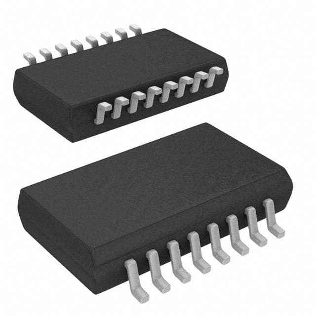
| 描述 | OPTOISO 2.5KV 2CH DRIVER 16SOIC数字隔离器 Prec Half-Bridge Dvr 0.1A Output |
| 产品分类 | |
| IsolatedPower | 无 |
| 品牌 | Analog Devices Inc |
| 产品手册 | |
| 产品图片 |
|
| rohs | 符合RoHS无铅 / 符合限制有害物质指令(RoHS)规范要求 |
| 产品系列 | 接口 IC,数字隔离器,Analog Devices ADUM1233BRWZiCoupler® |
| 数据手册 | |
| 产品型号 | ADUM1233BRWZ |
| PulseWidthDistortion(Max) | 8ns |
| 上升/下降时间(典型值) | 25ns, 25ns (最小值) |
| 不同If时的传播延迟高-低 | - |
| 产品目录页面 | |
| 产品种类 | |
| 传播延迟tpLH/tpHL(最大值) | 160ns, 160ns |
| 传播延迟时间 | 160 ns |
| 供应商器件封装 | 16-SOIC W |
| 共模瞬态抗扰度(最小值) | 75kV/µs |
| 其它图纸 |
|
| 包装 | 管件 |
| 商标 | Analog Devices |
| 安装类型 | 表面贴装 |
| 安装风格 | SMD/SMT |
| 封装 | Tube |
| 封装/外壳 | 16-SOIC(0.295",7.50mm 宽) |
| 封装/箱体 | SOIC-16 |
| 工作温度 | -40°C ~ 105°C |
| 工厂包装数量 | 47 |
| 技术 | 磁耦合 |
| 数据速率 | 10Mbps |
| 最大工作温度 | + 105 C |
| 最大数据速率 | 10 Mb/s |
| 最小工作温度 | - 40 C |
| 标准包装 | 47 |
| 电压-正向(Vf)(典型值) | - |
| 电压-电源 | 4.5 V ~ 5.5 V |
| 电压-隔离 | 2500Vrms |
| 电流-DC正向(If) | - |
| 电流-峰值输出 | 100mA |
| 电流-输出/通道 | - |
| 电流-输出高,低 | - |
| 类型 | General Purpose |
| 系列 | ADUM1233 |
| 绝缘电压 | 2.5 kVrms |
| 脉宽失真(最大) | 8ns |
| 视频文件 | http://www.digikey.cn/classic/video.aspx?PlayerID=1364138032001&width=640&height=505&videoID=2219593469001http://www.digikey.cn/classic/video.aspx?PlayerID=1364138032001&width=640&height=505&videoID=2219593470001http://www.digikey.cn/classic/video.aspx?PlayerID=1364138032001&width=640&height=505&videoID=2219614223001 |
| 认可 | UR, VDE |
| 输入-输入侧1/输入侧2 | 2/0 |
| 输入类型 | - |
| 输出类型 | 栅极驱动器 |
| 通道数 | 2 |
| 通道数量 | 2 Channel |


.jpg)

- 商务部:美国ITC正式对集成电路等产品启动337调查
- 曝三星4nm工艺存在良率问题 高通将骁龙8 Gen1或转产台积电
- 太阳诱电将投资9.5亿元在常州建新厂生产MLCC 预计2023年完工
- 英特尔发布欧洲新工厂建设计划 深化IDM 2.0 战略
- 台积电先进制程称霸业界 有大客户加持明年业绩稳了
- 达到5530亿美元!SIA预计今年全球半导体销售额将创下新高
- 英特尔拟将自动驾驶子公司Mobileye上市 估值或超500亿美元
- 三星加码芯片和SET,合并消费电子和移动部门,撤换高东真等 CEO
- 三星电子宣布重大人事变动 还合并消费电子和移动部门
- 海关总署:前11个月进口集成电路产品价值2.52万亿元 增长14.8%


PDF Datasheet 数据手册内容提取
Isolated, Precision Half-Bridge Driver, 0.1 A Output Data Sheet ADuM1233 FEATURES GENERAL DESCRIPTION Isolated high-side and low-side outputs The ADuM12331 is an isolated, half-bridge gate driver that High side or low side relative to input: ±700 VPEAK uses the Analog Devices, Inc., iCoupler® technology to provide High-side/low-side differential: 700 VPEAK independent and isolated high-side and low-side outputs. 0.1 A peak output current Combining high speed CMOS and monolithic transformer High frequency operation: 5 MHz maximum technology, this isolation component provides outstanding High common-mode transient immunity: >75 kV/µs performance characteristics superior to optocoupler-based High temperature operation: 105°C solutions. Wide body, 16-lead SOIC By avoiding the use of LEDs and photodiodes, this iCoupler gate Safety and regulatory approvals drive device is able to provide precision timing characteristics UL recognition not possible with optocouplers. Furthermore, the reliability and 2500 V rms for 1 minute per UL 1577 performance stability problems associated with optocoupler LEDs VDE certificate of conformity are avoided. DIN V VDE V 0884-10 (VDE V 0884-10): 2006-12 V = 560 V peak In comparison to gate drivers that use high voltage level translation IORM methodologies, the ADuM1233 offers the benefit of true, galvanic APPLICATIONS isolation between the input and each output. Each output can be Isolated IGBT/MOSFET gate drives operated up to ±700 VPEAK relative to the input, thereby supporting Plasma displays low-side switching to negative voltages. The differential voltage Industrial inverters between the high side and low side can be as high as 700 VPEAK. Switching power supplies As a result, the ADuM1233 provides reliable control over the switching characteristics of IGBT/MOSFET configurations over a wide range of positive or negative switching voltages. FUNCTIONAL BLOCK DIAGRAM VIA 1 16 VDDA VIB 2 ENCODE DECODE 15 VOA VDD1 3 14 GNDA GND1 4 13 NC DISABLE 5 12 NC NC 6 11 VDDB NC 7 ENCODE DECODE 10 VOB VDD1 8 9 GNDB 06271-001 Figure 1. 1 Protected by U.S. Patents 5,952,849; 6,873,065; 6,903,578; 7,075,329. Rev. C Information furnished by Analog Devices is believed to be accurate and reliable. However, no responsibility is assumed by Analog Devices for its use, nor for any infringements of patents or other One Technology Way, P.O. Box 9106, Norwood, MA 02062-9106, U.S.A. rights of third parties that may result from its use. Specifications subject to change without notice. No license is granted by implication or otherwise under any patent or patent rights of Analog Devices. Tel: 781.329.4700 www.analog.com Trademarks and registered trademarks are the property of their respective owners. Fax: 781.461.3113 ©2006–2012 Analog Devices, Inc. All rights reserved.
ADuM1233 Data Sheet TABLE OF CONTENTS Features .............................................................................................. 1 DIN V VDE V 0884-10 (VDE V 0884-10) Insulation Applications ....................................................................................... 1 Characteristics ...............................................................................5 General Description ......................................................................... 1 Recommended Operating Conditions .......................................5 Functional Block Diagram .............................................................. 1 Absolute Maximum Ratings ............................................................6 Revision History ............................................................................... 2 ESD Caution...................................................................................6 Specifications ..................................................................................... 3 Pin Configuration and Function Descriptions ..............................7 Electrical Characteristics ............................................................. 3 Typical Perfomance Characteristics ................................................8 Package Characteristics ............................................................... 4 Applications Information .................................................................9 Regulatory Information ............................................................... 4 Common-Mode Transient Immunity ........................................9 Insulation and Safety-Related Specifications ............................ 4 Outline Dimensions ....................................................................... 11 Ordering Guide .......................................................................... 11 REVISION HISTORY 8/12—Rev. B to Rev. C 12/07—Rev. A to Rev. B Changes to Features Section............................................................ 1 Changes to Note 1 ............................................................................. 1 Created Hyperlink for Safety and Regulatory Approvals Change to Minimum Pulse Width .................................................. 3 Entry in Features Section ................................................................. 1 Changed IC Junction-to-Ambient Thermal Resistance 4/07—Rev. Sp0: Rev. A Parameter in Table 2 ......................................................................... 4 Changes to Figure 1 ........................................................................... 1 Changes to Table 3 and Table 4 ....................................................... 4 Changes to Figure 7 ........................................................................... 7 Added DIN V VDE V 0884-10 (VDE V 0884-10) Insulation Updated Outline Dimensions ....................................................... 10 Characteristics Section ..................................................................... 5 Added Table 5 and Figure 2; Renumbered Sequentially ............. 5 7/06—Revision Sp0: Initial Version Updated Outline Dimensions ....................................................... 11 Rev. C | Page 2 of 12
Data Sheet ADuM1233 SPECIFICATIONS ELECTRICAL CHARACTERISTICS All voltages are relative to their respective ground. 4.5 V ≤ V ≤ 5.5 V, 12 V ≤ V ≤ 18 V, and 12 V ≤ V ≤ 18 V. All minimum/ DD1 DDA DDB maximum specifications apply over the entire recommended operating range, unless otherwise noted. All typical specifications are at T = 25°C, V = 5 V, V = 15 V, and V = 15 V. A DD1 DDA DDB Table 1. Parameter Symbol Min Typ Max Unit Test Conditions/Comments DC SPECIFICATIONS Input Supply Current (V Pins) DD1 Quiescent I 3.0 4.2 mA DDI(Q) 10 Mbps I 6.0 9.0 mA DDI(10) Output Supply Current (V and V Pins) DDA DDB Quiescent I , I 0.3 1.2 mA DDA(Q) DDB(Q) 10 Mbps I , I 16 22 mA C = 200 pF DDA(10) DDB(10) L Input Currents I , I , I −10 +0.01 +10 µA 0 V ≤ V , V , V ≤ V IA IB DISABLE IA IB DISABLE DD1 Logic High Input Threshold V 2.0 V IH Logic Low Input Threshold V 0.8 V IL Logic High Output Voltages V , V V − 0.1, V , V V I , I = −1 mA OAH OBH DDA DDA DDB OA OB V − 0.1 DDB Logic Low Output Voltages V , V 0.1 V I , I = +1 mA OAL OBL OA OB Output Short-Circuit Pulsed Current1 I , I 100 mA OA(SC) OB(SC) SWITCHING SPECIFICATIONS C = 200 pF L Minimum Pulse Width2 PW 80 ns Maximum Switching Frequency3 10 Mbps Propagation Delay4 t , t 97 124 160 ns PHL PLH Change vs. Temperature 100 ps/°C Pulse Width Distortion, |t − t | PWD 8 ns PLH PHL Channel-to-Channel Matching, 5 ns Rising or Falling Edges5 Channel-to-Channel Matching, 13 ns Rising vs. Falling Edges6 Part-to-Part Matching, Rising or Falling Edges7 55 ns Input t = 3 ns R Part-to-Part Matching, Rising vs. Falling Edges8 63 ns Input t = 3 ns R Output Rise/Fall Time (10% to 90%) t/t 25 ns R F 1 Short-circuit duration less than one second. 2 The minimum pulse width is the shortest pulse width at which the specified timing parameters are guaranteed. 3 The maximum switching frequency is the maximum signal frequency at which the specified timing parameters are guaranteed. 4 tPHL propagation delay is measured from the 50% level of the falling edge of the VIx signal to the 50% level of the falling edge of the VOx signal. tPLH propagation delay is measured from the 50% level of the rising edge of the VIx signal to the 50% level of the rising edge of the VOx signal. 5 Channel-to-channel matching, rising or falling edges is the magnitude of the propagation delay difference between two channels of the same part when the inputs are either both rising or falling edges. The supply voltages and the loads on each channel are equal. 6 Channel-to-channel matching, rising vs. falling edges is the magnitude of the propagation delay difference between two channels of the same part when one input is a rising edge and the other input is a falling edge. The supply voltages and loads on each channel are equal. 7 Part-to-part matching, rising or falling edges is the magnitude of the propagation delay difference between the same channels of two different parts when the inputs are either both rising or falling edges. The supply voltages, temperatures, and loads of each part are equal. 8 Part-to-part matching, rising vs. falling edges is the magnitude of the propagation delay difference between the same channels of two different parts when one input is a rising edge and the other input is a falling edge. The supply voltages, temperatures, and loads of each part are equal. Rev. C | Page 3 of 12
ADuM1233 Data Sheet PACKAGE CHARACTERISTICS Table 2. Parameter Symbol Min Typ Max Unit Test Conditions/Comments Resistance (Input-to-Output)1 R 1012 Ω I-O Capacitance (Input-to-Output)1 C 2.0 pF f = 1 MHz I-O Input Capacitance C 4.0 pF I IC Junction-to-Ambient Thermal Resistance θ 45 °C/W JA 1 The device is considered a two-terminal device: Pin 1 through Pin 8 are shorted together, and Pin 9 through Pin 16 are shorted together. REGULATORY INFORMATION The ADuM1233 is approved by the organizations listed in Table 3. Table 3. UL VDE Recognized Under 1577 Component Recognition Program1 Certified according to DIN V VDE V 0884-10 (VDE V 0884-10): 2006-122 Single/Basic 2500 V rms Isolation Voltage Reinforced insulation, 560 V peak File E214100 File 2471900-4880-0001 1 In accordance with UL 1577, each ADuM1233 is proof tested by applying an insulation test voltage ≥ 3000 V rms for 1 second (current leakage detection limit = 5 µA). 2 In accordance with DIN V VDE V 0884-10, each ADuM1233 is proof tested by applying an insulation test voltage ≥ 1050 V peak for 1 second (partial discharge detection limit = 5 pC). The asterisk (*) marking branded on the component designates DIN V VDE V 0884-10 approval. INSULATION AND SAFETY-RELATED SPECIFICATIONS Table 4. Parameter Symbol Value Unit Test Conditions/Comments Rated Dielectric Insulation Voltage 2500 V rms 1 minute duration Minimum External Air Gap (Clearance) L(I01) 3.5 min mm Measured from input terminals to output terminals, shortest distance through air Minimum External Tracking (Creepage) L(I02) 3.5 min mm Measured from input terminals to output terminals, shortest distance path along body Minimum Internal Gap (Internal Clearance) 0.017 min mm Insulation distance through insulation Tracking Resistance (Comparative Tracking Index) CTI >175 V DIN IEC 112/VDE 0303 Part 1 Isolation Group IIIa Material Group (DIN VDE 0110, 1/89, Table 1) Rev. C | Page 4 of 12
Data Sheet ADuM1233 DIN V VDE V 0884-10 (VDE V 0884-10) INSULATION CHARACTERISTICS This isolator is suitable for reinforced isolation only within the safety limit data. Maintenance of the safety data is ensured by protective circuits. The asterisk (*) marking on the package denotes DIN V VDE V 0884-10 approval for a 560 V peak working voltage. Table 5. Description Test Conditions/Comments Symbol Characteristic Unit Installation Classification per DIN VDE 0110 For Rated Mains Voltage ≤ 150 V rms I to IV For Rated Mains Voltage ≤ 300 V rms I to III For Rated Mains Voltage ≤ 400 V rms I to II Climatic Classification 40/105/21 Pollution Degree per DIN VDE 0110, Table 1 2 Maximum Working Insulation Voltage V 560 V peak IORM Input-to-Output Test Voltage, Method B1 V × 1.875 = V , 100% production test, V 1050 V peak IORM pd(m) pd(m) t = t = 1 sec, partial discharge < 5 pC ini m Input-to-Output Test Voltage, Method A After Environmental Tests Subgroup 1 V × 1.5 = V , t = 60 sec, t = 10 sec, V 896 V peak IORM pd(m) ini m pd(m) partial discharge < 5 pC After Input and/or Safety Tests Subgroup 2 V × 1.2 = V , t = 60 sec, t = 10 sec, V 672 V peak IORM pd(m) ini m pd(m) and Subgroup 3 partial discharge < 5 pC Highest Allowable Overvoltage V 4000 V peak IOTM Surge Isolation Voltage V peak = 10 kV, 1.2 µs rise time, 50 µs, 50% fall time V 4000 V peak IOSM Safety-Limiting Values Maximum value allowed in the event of a failure (see Figure 2) Case Temperature T 150 °C S Safety Total Dissipated Power P 1 W S Insulation Resistance at T V = 500 V R >109 Ω S IO S 1.2 RECOMMENDED OPERATING CONDITIONS W)1.0 Table 6. R ( Parameter Symbol Min Max Unit E W PO0.8 Operating Temperature TA −40 +105 °C G Input Supply Voltage1 V 4.5 5.5 V N DD1 MITI0.6 Output Supply Voltages1 VDDA, 12 18 V E LI VDDB F SA0.4 Input Signal Rise and Fall Times 100 ns Common-Mode Transient Immunity 0.2 Input-to-Output2 −75 +75 kV/µs Between Outputs2 −75 +75 kV/µs 00 50AMBIENT TEM10P0ERATURE (°C1)50 200 06271-102 TraVnosliteangte Ism2 munity, Supply −75 +75 kV/µs Figure 2. Thermal Derating Curve, Dependence of Safety-Limiting Values on Case Temperature, per DIN V VDE V 0884-10 1 All voltages are relative to their respective ground. 2 See the Common-Mode Transient Immunity section for more information. Rev. C | Page 5 of 12
ADuM1233 Data Sheet ABSOLUTE MAXIMUM RATINGS Ambient temperature = 25°C, unless otherwise noted. Stresses above those listed under Absolute Maximum Ratings may cause permanent damage to the device. This is a stress Table 7. rating only; functional operation of the device at these or any Parameter Rating other conditions above those indicated in the operational Storage Temperature (T ) −55°C to +150°C ST section of this specification is not implied. Exposure to absolute Ambient Operating Temperature (T) −40°C to +105°C A maximum rating conditions for extended periods may affect Input Supply Voltage1 (V ) −0.5 V to +7.0 V DD1 device reliability. Output Supply Voltage1 (V , V ) −0.5 V to +27 V DDA DDB Input Voltage1 (V , V ) −0.5 V to V + 0.5 V IA IB DDI ESD CAUTION Output Voltage1 V −0.5 V to V + 0.5 V OA DDA V −0.5 V to V + 0.5 V OB DDB Input-to-Output Voltage2 −700 V to +700 V PEAK PEAK Output Differential Voltage3 +700 V PEAK Output DC Current (I , I ) −20 mA to +20 mA OA OB Common-Mode Transients4 −100 kV/µs to +100 kV/µs 1 All voltages are relative to their respective ground. 2 Input-to-output voltage is defined as GNDA − GND1 or GNDB − GND1. 3 Output differential voltage is defined as GNDA − GNDB. 4 Refers to common-mode transients across any insulation barrier. Common- mode transients exceeding the Absolute Maximum Ratings may cause latch-up or permanent damage. Rev. C | Page 6 of 12
Data Sheet ADuM1233 PIN CONFIGURATION AND FUNCTION DESCRIPTIONS VIA 1 16 VDDA VIB 2 15 VOA VDD1 3 ADuM1233 14 GNDA GND1 4 TOP VIEW 13 NC DISABLE 5 (Not to Scale) 12 NC NC 6 11 VDDB NC 7 10 VOB VDD1 8NC = NO CONNECT9 GNDB 06271-002 Figure 3. Pin Configuration Table 8. Pin Function Descriptions Pin No. Mnemonic Description 1 V Logic Input A. IA 2 V Logic Input B. IB 3, 81 V Input Supply Voltage, 4.5 V to 5.5 V. DD1 4 GND Ground Reference for Input Logic Signals. 1 5 DISABLE Input Disable. Disables the isolator inputs and refresh circuits. Outputs take on default low state. 6, 7, 12, 132 NC No Connect. 9 GND Ground Reference for Output B. B 10 V Output B. OB 11 V Output B Supply Voltage, 12 V to 18 V. DDB 14 GND Ground Reference for Output A. A 15 V Output A. OA 16 V Output A Supply Voltage, 12 V to 18 V. DDA 1 Pin 3 and Pin 8 are internally connected. Connecting both pins to VDD1 is recommended. 2 Pin 12 and Pin 13 are floating and should be left unconnected. Table 9. Truth Table (Positive Logic) V /V Input V State DISABLE V /V Output Notes IA IB DD1 OA OB High Powered Low High Low Powered Low Low X1 Unpowered X1 Low Output returns to input state within 1 µs of V power restoration. DD1 X1 Powered High Low 1 X is don’t care. Rev. C | Page 7 of 12
ADuM1233 Data Sheet TYPICAL PERFOMANCE CHARACTERISTICS 7 115 6 114 RENT (mA) 54 N DELAY (ns) 111132 CH. B,FALLING EDGE R O CU 3 ATI CH.A,FALLING EDGE T G U A 111 P P N 2 O I R P CH.A, RISING EDGE 110 1 CH. B, RISING EDGE 00 DATA RAT4E (Mbps) 10 06271-006 10912 OUTPUT SUPP1L5Y VOLTAGE (V) 18 06271-009 Figure 4. Typical Input Supply Current Variation with Data Rate Figure 7. Typical Propagation Delay Variation with Output Supply Voltage (Input Supply Voltage = 5.0 V) 18 115 16 114 14 A) ns) ENT (m 1120 DELAY ( 113 CH. B,FALLING EDGE RR N 112 CU 8 TIO CH.A,FALLING EDGE UT GA P 6 A 111 T P U O O R 4 P CH.A, RISING EDGE 110 2 CH. B, RISING EDGE 00 DATA RAT4E (Mbps) 10 06271-007 1094.5 INPUT SUPPL5Y.0 VOLTAGE (V) 5.5 06271-010 Figure 5. Typical Output Supply Current Variation with Data Rate Figure 8. Typical Propagation Delay Variation with Input Supply Voltage (Output Supply Voltage = 15.0 V) 120 s) 115 n Y ( A L E D N 110 O TI A G A P O R 105 P 100–40 –20 0 T2E0MPERA40TURE (6°0C) 80 100 120 06271-008 Figure 6. Typical Propagation Delay Variation with Temperature Rev. C | Page 8 of 12
Data Sheet ADuM1233 APPLICATIONS INFORMATION COMMON-MODE TRANSIENT IMMUNITY The transient magnitude of the sinusoidal component is given by In general, common-mode transients consist of linear and dVCM/dt = 2πf V0 sinusoidal components. The linear component of a common- The ability of the ADuM1233 to operate correctly in the presence mode transient is given by of sinusoidal transients is characterized by the data in Figure 10 V = (ΔV/Δt) t and Figure 11. The data is based on design simulation and is the CM, linear maximum sinusoidal transient magnitude (2πf V) that the where ΔV/Δt is the slope of the transient shown in Figure 12 0 ADuM1233 can tolerate without an operational error. Values and Figure 13. for immunity against sinusoidal transients are not included in The transient of the linear component is given by Table 6 because measurements to obtain such values have not dV /dt = ΔV/Δt been possible. CM The ability of the ADuM1233 to operate correctly in the 300 presence of linear transients is characterized by the data in Figure 9. The data is based on design simulation and is the 250 maximum linear transient magnitude that the ADuM1233 can V/µs) BEST-CASE PROCESSVARIATION tolerate without an operational error. This data shows a higher Y (k 200 T level of robustness than what is listed in Table 6 because the NI U transient immunity values obtained in Table 6 use measured M 150 M data and apply allowances for measurement error and margin. T I N 400 NSIE 100 A R 350 T 50 TY (kV/µs) 320500 BEST-CASE PROCESSVARIATION 00 250 500 WOF75RR0ESQT-UCE1A0NS0CE0Y P (RM1OH2C5zE0)SS1V5A0R0IATI1O7N50 2000 06271-012 UNI Figure 10. Transient Immunity (Sinusoidal Transients), M 200 M 27°C Ambient Temperature T I EN 150 250 NSI WORST-CASE PROCESSVARIATION A 100 R T 200 50 s) µ V/ 0–40 –20 0 TEM2P0ERATUR4E0 (°C) 60 80 100 06271-011 UNITY (k 150 BEST-CASE PROCESSVARIATION M Figure 9. Transient Immunity (Linear Transients) vs. Temperature M T I 100 N The sinusoidal component (at a given frequency) is given by E SI N VCM, sinusoidal = V0sin(2πft) TRA 50 where: V is the magnitude of the sinusoidal. WORST-CASE PROCESSVARIATION f i0s the frequency of the sinusoidal. 00 250 500 F75R0EQUE10N0C0Y (M1H25z0) 1500 1750 2000 06271-013 Figure 11. Transient Immunity (Sinusoidal Transients), 100°C Ambient Temperature Rev. C | Page 9 of 12
ADuM1233 Data Sheet 15V VDD1 5V GND1 VDDAANDVDDB 15V GNDAAND GNDB 15V ΔV VDDAANDVDDB Δt ΔV GNDAAND GNDB VDD1 5V Δt 15V GND1 06271-003 Figure 12. Common-Mode Transient Immunity Waveforms—Input to Output 15V VDDA/VDDB 15V GNDA/GNDB VDDB/VDDA 15V GNDB/GNDA 15V ΔV VDDA/VDDB Δt ΔV GNDA/GNDB VDDB/VDDA 15V Δt 15V GNDA/GNDB 06271-004 Figure 13. Common-Mode Transient Immunity Waveforms—Between Outputs VDDA/VDDB ΔVDD Δt VGDNDDAA/V/GDNDBDB GNDA/GNDB 06271-005 Figure 14. Transient Immunity Waveforms—Output Supplies Rev. C | Page 10 of 12
Data Sheet ADuM1233 OUTLINE DIMENSIONS 10.50(0.4134) 10.10(0.3976) 16 9 7.60(0.2992) 7.40(0.2913) 1 8 10.65(0.4193) 10.00(0.3937) 1.27(0.0500) 0.75(0.0295) BSC 2.65(0.1043) 0.25(0.0098) 45° 0.30(0.0118) 2.35(0.0925) 8° 0.10(0.0039) 0° COPLANARITY 0.10 0.51(0.0201) SPELAATNIENG 0.33(0.0130) 1.27(0.0500) 0.31(0.0122) 0.20(0.0079) 0.40(0.0157) C(RINOEFNPEATRRREOENNLCLTEIHNCEOGOSNDMELISPYM)LAEAIANNRNDSETIAORTRNOOESUJNANEORDDETEEDAICN-POSMPFTRIFALONLMPIDMIRLAELIRATIMTDEEESRTFSMEO;SRIRN-0ECU1QH3SU-EADIVAIINMAELDENENSSTIIOGSNNFS.OR 03-27-2007-B Figure 15. 16-Lead Standard Small Outline Package [SOIC_W] Wide Body (RW-16) Dimensions shown in millimeters and (inches) ORDERING GUIDE No. of Output Peak Output Package Model1 Channels Current (A) Voltage (V) Temperature Range Package Description Option ADuM1233BRWZ 2 0.1 15 −40°C to +105°C 16-Lead SOIC_W RW-16 ADuM1233BRWZ-RL 2 0.1 15 −40°C to +105°C 16-Lead SOIC_W, 13-Inch Tape RW-16 and Reel Option (1,000 Units) 1 Z = RoHS Compliant Part. Rev. C | Page 11 of 12
ADuM1233 Data Sheet NOTES ©2006–2012 Analog Devices, Inc. All rights reserved. Trademarks and registered trademarks are the property of their respective owners. D06271-0-8/12(C) Rev. C | Page 12 of 12
Mouser Electronics Authorized Distributor Click to View Pricing, Inventory, Delivery & Lifecycle Information: A nalog Devices Inc.: ADUM1233BRWZ ADUM1233BRWZ-RL