ICGOO在线商城 > SY10E451JY
 Datasheet下载
- 型号: SY10E451JY
- 制造商: Micrel
- 库位|库存: xxxx|xxxx
- 要求:
| 数量阶梯 | 香港交货 | 国内含税 |
| +xxxx | $xxxx | ¥xxxx |
查看当月历史价格
查看今年历史价格
SY10E451JY产品简介:
ICGOO电子元器件商城为您提供SY10E451JY由Micrel设计生产,在icgoo商城现货销售,并且可以通过原厂、代理商等渠道进行代购。 提供SY10E451JY价格参考以及MicrelSY10E451JY封装/规格参数等产品信息。 你可以下载SY10E451JY参考资料、Datasheet数据手册功能说明书, 资料中有SY10E451JY详细功能的应用电路图电压和使用方法及教程。
SY10E451JY 是 Microchip Technology(原收购了Micrel)推出的高速ECL(发射极耦合逻辑)双D型触发器,工作于-4.5V至-5.2V负电源,典型传播延迟低至0.6ns,支持高达3GHz的时钟频率。其主要应用场景包括:
1. 高速通信系统:用于光纤收发器、SONET/SDH、10G以太网等设备中的数据采样、同步和时序对齐;
2. 测试与测量仪器:在高速示波器、误码率测试仪(BERT)中实现精确边沿触发、数据锁存与信号重建;
3. 雷达与军事电子:满足严苛时序要求的脉冲处理、T/R开关控制及时钟分频/延时电路;
4. 高性能计算与时钟管理:作为低抖动寄存器,用于FPGA/CPU外围的高速接口同步(如源同步DDR控制信号锁存);
5. 射频与微波子系统:配合高速DAC/ADC完成数字基带信号的时序整形与相位控制。

该器件采用JEDEC标准SOIC-20宽体封装(JY后缀),具备差分ECL输入/输出,兼容PECL电平,支持热插拔及高抗噪性,适用于-40°C至+85°C工业级环境。需注意其负电源供电特性及终端匹配要求(通常需50Ω至VCC或地)。目前已逐步被更集成、更低功耗的SiGe或CMOS替代,但在部分遗留高端射频/军工平台中仍有应用。
| 参数 | 数值 |
| 产品目录 | 集成电路 (IC) |
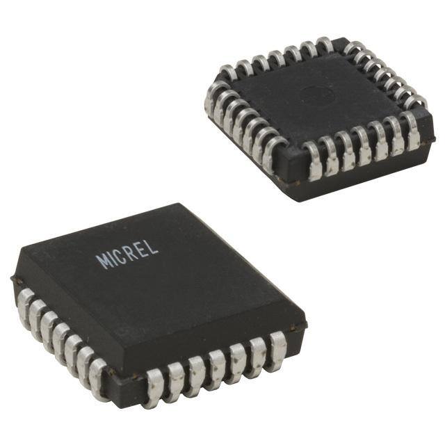
| 描述 | IC D-TYPE POS TRG SNGL 28PLCC |
| 产品分类 | |
| 品牌 | Micrel Inc |
| 数据手册 | |
| 产品图片 |
|
| 产品型号 | SY10E451JY |
| rohs | 无铅 / 符合限制有害物质指令(RoHS)规范要求 |
| 产品系列 | 10E |
| 不同V、最大CL时的最大传播延迟 | - |
| 产品目录页面 | |
| 元件数 | 1 |
| 其它名称 | 576-2019-5 |
| 功能 | 主复位 |
| 包装 | 管件 |
| 安装类型 | 表面贴装 |
| 封装/外壳 | 28-LCC(J 形引线) |
| 工作温度 | -40°C ~ 85°C (TA) |
| 标准包装 | 38 |
| 每元件位数 | 6 |
| 电压-电源 | -4.2 V ~ -5.5 V |
| 电流-输出高,低 | - |
| 电流-静态 | 101mA |
| 类型 | D 型 |
| 触发器类型 | 正,负 |
| 输入电容 | - |
| 输出类型 | 非反相 |
| 频率-时钟 | 1.4GHz |


- 商务部:美国ITC正式对集成电路等产品启动337调查
- 曝三星4nm工艺存在良率问题 高通将骁龙8 Gen1或转产台积电
- 太阳诱电将投资9.5亿元在常州建新厂生产MLCC 预计2023年完工
- 英特尔发布欧洲新工厂建设计划 深化IDM 2.0 战略
- 台积电先进制程称霸业界 有大客户加持明年业绩稳了
- 达到5530亿美元!SIA预计今年全球半导体销售额将创下新高
- 英特尔拟将自动驾驶子公司Mobileye上市 估值或超500亿美元
- 三星加码芯片和SET,合并消费电子和移动部门,撤换高东真等 CEO
- 三星电子宣布重大人事变动 还合并消费电子和移动部门
- 海关总署:前11个月进口集成电路产品价值2.52万亿元 增长14.8%


PDF Datasheet 数据手册内容提取
NOT RECOMMENDED FOR NEW DESIGNS SY10E451 Micrel, Inc. 6-BIT REGISTER SY1S0YE10405E1451 DIFFERENTIAL DATA CLOCK SY100E451 FEATURES DESCRIPTION (cid:1) 1100MHz min. toggle frequency The SY10/100E451 offer six D-type flip-flops with single- (cid:1) Extended 100E V range of –4.2V to –5.5V ended outputs and differential data and clock inputs, EE designed for use in new, high-performance ECL systems. (cid:1) Differential inputs: data and clock The registers are triggered by the rising edge of the CLK (cid:1) VBB output for single-ended use input. (cid:1) Asynchronous Master Reset A logic HIGH on the Master Reset (MR) input resets all (cid:1) Fully compatible with industry standard 10KH, outputs to a logic LOW. The VBB output is provided for use 100K ECL levels as a reference voltage for single-ended reception of ECL (cid:1) Internal 75KΩ input pulldown resistors signals to that device only. When used for this purpose, it is recommended that V is decoupled to V via a 0.01µF (cid:1) Fully compatible with Motorola MC10E/100E451 capacitor. BB CC (cid:1) Available in 28-pin PLCC package BLOCK DIAGRAM PIN NAMES Pin Function D /D0 D Q0 D0–D5 +Data Input 0 R /D0–/D5 –Data Input CLK +Clock Input D 1 /D1 D Q1 /CLK –Clock Input R Q0–Q5 Data Outputs D 2 MR Master Reset Input /D D Q2 2 V V Output R BB BB V V to Output D CCO CC 3 /D D Q3 3 R D 4 /D D Q4 4 R D 5 /D D Q5 5 R CLK /CLK MR V BB M9999-032206 Rev.: G Amendment: /0 1 hbwhelp@micrel.com or (408) 955-1690 Issue Date: March 2006
SY10E451 Micrel, Inc. SY100E451 PACKAGE/ORDERING INFORMATION Ordering Information(1) O C Package Operating Package Lead /D5 D5 /D4 D4 /D3 D3 VC Part Number Type Range Marking Finish SY10E451JI J28-1 Industrial SY10E451JI Sn-Pb 25 24 23 22 21 20 19 CLK 26 18 Q5 SY10E451JITR(2) J28-1 Industrial SY10E451JI Sn-Pb VBB 27 17 Q4 SY100E451JI J28-1 Industrial SY100E451JI Sn-Pb /CLK 28 16 VCC TOP VIEW SY100E451JITR(2) J28-1 Industrial SY100E451JI Sn-Pb VEE 1 PLCC 15 Q3 MR 2 J28-1 14 VCCO SY10E451JC J28-1 Commercial SY10E451JC Sn-Pb NC 3 13 Q2 SY10E451JCTR(2) J28-1 Commercial SY10E451JC Sn-Pb D0 4 12 Q1 SY100E451JC J28-1 Commercial SY100E451JC Sn-Pb 5 6 7 8 9 10 11 SY100E451JCTR(2) J28-1 Commercial SY100E451JC Sn-Pb 0 1 1 2 2 O 0 /D D /D D /D VCC Q SY10E451JY(3) J28-1 Industiral SY10E451JY with Matte-Sn Pb-Free bar-line indicator 28-Pin PLCC (J28-1) SY10E451JYTR(2, 3) J28-1 Industrial SY10E451JY with Matte-Sn Pb-Free bar-line indicator SY100E451JY(3) J28-1 Industrial SY100E451JY with Matte-Sn Pb-Free bar-line indicator SY100E451JYTR(2, 3) J28-1 Industrial SY100E451JY with Matte-Sn Pb-Free bar-line indicator Notes: 1. Contact factory for die availability. Dice are guaranteed at T = 25°C, DC Electricals only. A 2. Tape and Reel. 3. Pb-Free package is recommended for new designs. M9999-032206 2 hbwhelp@micrel.com or (408) 955-1690
SY10E451 Micrel, Inc. SY100E451 DC ELECTRICAL CHARACTERISTICS V = V (Min.) to V (Max.); V = V = GND EE EE EE CC CCO TA = –40°C TA = 0°C TA = 25°C TA = +85°C Symbol Parameter Min. Typ. Max. Min. Typ. Max. Min. Typ. Max. Min. Typ. Max. Unit V Output Reference 10E –1.38 — –1.27 –1.35 — –1.25 –1.31 — –1.19 V BB Voltage 100E –1.38 — –1.26 –1.38 — –1.26 –1.38 — –1.26 I Input HIGH Current — — 150 — — 150 — — 150 µA IH I Power Supply 10E — 84 101 — 84 101 — 84 101 mA EE Current 100E — 84 101 — 84 101 — 97 116 V Common Mode Range(1) –2.0 — –0.4 –2.0 — –0.4 –2.0 — –0.4 V CMR Note: 1. V is referenced to the most psitive side of the differential input signal. Normal operation is obtained when the “HIGH” input is within the V range CMR CMR and the input swing is greater than V (min) and <1V. PP AC ELECTRICAL CHARACTERISTICS V = V (Min.) to V (Max.); V = V = GND EE EE EE CC CCO TA = –40°C TA = 0°C TA = 25°C TA = +85°C Symbol Parameter Min. Typ. Max. Min. Typ. Max. Min. Typ. Max. Min. Typ. Max. Unit f Max. Toggle Frequency 1100 1400 — 1100 1400 — 1100 1400 — MHz MAX t Propagation Delay to ps PD Output CLK (Diff) 475 650 800 475 650 800 475 650 800 CLK (SE) 425 650 850 425 650 850 425 650 850 MR 425 600 850 425 600 850 425 600 850 t Set-up Time D 150 –100 — 150 –100 — 150 –100 — ps S t Hold Time D 250 100 — 250 100 — 250 100 — ps H V Minimum Input Swing(1) 150 — — 150 — — 150 — — mV PP(AC) t Reset Recovery Time 750 600 — 750 600 — 750 600 — ps RR t Minimum Pulse Width 400 — — 400 — — 400 — — ps PW CLK, MR t Within-Device Skew(2) — 100 — — 100 — — 100 — ps skew t Rise/Fall Time 275 450 800 275 450 800 275 450 800 ps r t 20% to 80% f Notes: 1. Minimum input voltage for which AC parameters are guaranteed. 2. Within-device skew is defined as identical transitions on similar paths through a device. M9999-032206 3 hbwhelp@micrel.com or (408) 955-1690
SY10E451 Micrel, Inc. SY100E451 28-PIN PLCC (J28-1) Rev. 03 MICREL, INC. 2180 FORTUNE DRIVE SAN JOSE, CA 95131 USA TEL + 1 (408) 944-0800 FAX + 1 (408) 474-1000 WEB http://www.micrel.com The information furnished by Micrel in this data sheet is believed to be accurate and reliable. However, no responsibility is assumed by Micrel for its use. Micrel reserves the right to change circuitry and specifications at any time without notification to the customer. Micrel Products are not designed or authorized for use as components in life support appliances, devices or systems where malfunction of a product can reasonably be expected to result in personal injury. Life support devices or systems are devices or systems that (a) are intended for surgical implant into the body or (b) support or sustain life, and whose failure to perform can be reasonably expected to result in a significant injury to the user. A Purchaser’s use or sale of Micrel Products for use in life support appliances, devices or systems is at Purchaser’s own risk and Purchaser agrees to fully indemnify Micrel for any damages resulting from such use or sale. © 2006 Micrel, Incorporated. M9999-032206 4 hbwhelp@micrel.com or (408) 955-1690