ICGOO在线商城 > SUP75N03-04-E3
 Datasheet下载
- 型号: SUP75N03-04-E3
- 制造商: Vishay
- 库位|库存: xxxx|xxxx
- 要求:
| 数量阶梯 | 香港交货 | 国内含税 |
| +xxxx | $xxxx | ¥xxxx |
查看当月历史价格
查看今年历史价格
SUP75N03-04-E3产品简介:
ICGOO电子元器件商城为您提供SUP75N03-04-E3由Vishay设计生产,在icgoo商城现货销售,并且可以通过原厂、代理商等渠道进行代购。 提供SUP75N03-04-E3价格参考以及VishaySUP75N03-04-E3封装/规格参数等产品信息。 你可以下载SUP75N03-04-E3参考资料、Datasheet数据手册功能说明书, 资料中有SUP75N03-04-E3详细功能的应用电路图电压和使用方法及教程。
| 参数 | 数值 |
| 产品目录 | |
| ChannelMode | Enhancement |
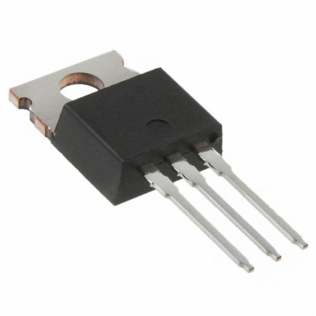
| 描述 | MOSFET N-CH 30V 75A TO220ABMOSFET 30V 75A 187W |
| 产品分类 | FET - 单分离式半导体 |
| FET功能 | 逻辑电平门 |
| FET类型 | MOSFET N 通道,金属氧化物 |
| Id-ContinuousDrainCurrent | 75 A |
| Id-连续漏极电流 | 75 A |
| 品牌 | Vishay / SiliconixVishay Siliconix |
| 产品手册 | |
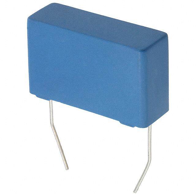
| 产品图片 |
|
| rohs | RoHS 合规性豁免无铅 / 符合限制有害物质指令(RoHS)规范要求 |
| 产品系列 | 晶体管,MOSFET,Vishay / Siliconix SUP75N03-04-E3TrenchFET® |
| 数据手册 | |
| 产品型号 | SUP75N03-04-E3SUP75N03-04-E3 |
| Pd-PowerDissipation | 187 W |
| Pd-功率耗散 | 187 W |
| RdsOn-Drain-SourceResistance | 7 mOhms |
| RdsOn-漏源导通电阻 | 7 mOhms |
| Vds-Drain-SourceBreakdownVoltage | 30 V |
| Vds-漏源极击穿电压 | 30 V |
| Vgs-Gate-SourceBreakdownVoltage | +/- 20 V |
| Vgs-栅源极击穿电压 | 20 V |
| 上升时间 | 40 ns |
| 下降时间 | 95 ns |
| 不同Id时的Vgs(th)(最大值) | 3V @ 250µA |
| 不同Vds时的输入电容(Ciss) | 10742pF @ 25V |
| 不同Vgs时的栅极电荷(Qg) | 250nC @ 10V |
| 不同 Id、Vgs时的 RdsOn(最大值) | 4 毫欧 @ 75A,10V |
| 产品种类 | MOSFET |
| 供应商器件封装 | TO-220AB |
| 其它名称 | SUP75N03-04-E3CT |
| 典型关闭延迟时间 | 190 ns |
| 功率-最大值 | 3.7W |
| 包装 | 散装 |
| 商标 | Vishay / Siliconix |
| 商标名 | TrenchFET |
| 安装类型 | 通孔 |
| 安装风格 | Through Hole |
| 封装 | Tube |
| 封装/外壳 | TO-220-3 |
| 封装/箱体 | TO-220-3 |
| 工厂包装数量 | 50 |
| 晶体管极性 | N-Channel |
| 最大工作温度 | + 175 C |
| 最小工作温度 | - 55 C |
| 标准包装 | 500 |
| 漏源极电压(Vdss) | 30V |
| 电流-连续漏极(Id)(25°C时) | 75A (Tc) |
| 通道模式 | Enhancement |
| 配置 | Single |


.jpg)


PDF Datasheet 数据手册内容提取
SUP/SUB75N03-04 Vishay Siliconix N-Channel 30-V (D-S), 175 °C MOSFET FEATURES PRODUCT SUMMARY • TrenchFET® Power MOSFETs V (V) r (Ω) I (A) (BR)DSS DS(on) D (cid:129) 175 °C Rated Maximum Junction Available 30 0.004 75a RoHS* Temperature COMPLIANT TO-220AB D TO-263 DRAIN connected to TAB DRAIN connected to TAB G D S G Top View G D S SUB75N03-04 Top View SUP75N03-04 S Ordering Information:SUP75N03-04 SUP75N03-04-E3 (Lead (Pb)-free) SUB75N03-04 N-ChannelMOSFET SUB75N03-04-E3 (Lead (Pb)-free) ABSOLUTE MAXIMUM RATINGS T = 25°C, unless otherwise noted C Parameter Symbol Limit Unit Gate-Source Voltage VGS ± 20 V TC = 25 °C 75a Continuous Drain Current (T = 175 °C) I J D TC = 125 °C 75a Pulsed Drain Current IDM 250 A Pulse Diode Forward Current ISM 250 Continuous Source Current (Diode Conduction) IS 75 Avalanche Current IAR 75 Avalanche Energy L = 0.1 mH EAS 280 mJ Repetitive Avalanche Energyb L = 0.05 mH EAR 140 TC = 25 °C (TO-220AB and TO-263) 187c Maximum Power Dissipation T = 25 °C (TO-263)d PD 3.7 W A Operating Junction and Storage Temperature Range TJ, Tstg - 55 to 175 °C Lead Temperature (1/16" from case for 10 sec.) TO-220AB TL 300 THERMAL RESISTANCE RATINGS Parameter Symbol Limit Unit PCB Mount (TO-263)d 40 Junction-to-Ambient RthJA Free Air (TO-220AB) 62.5 °C/W Junction-to-Case RthJC 0.6 Notes: a. Package limited. b. Duty cycle ≤ 1 %. c. See SOA curve for voltage derating. d. When Mounted on 1" square PCB (FR-4 material). For SPICE model information via the Worldwide Web: http://www.vishay.com/www/product/spice.htm. * Pb containing terminations are not RoHS compliant, exemptions may apply Document Number: 70745 www.vishay.com S-62484-Rev. F, 04-Dec-06 1
SUP/SUB75N03-04 Vishay Siliconix SPECIFICATIONS T = 25°C, unless otherwise noted J Parameter Symbol Test Conditions Min Typa Max Unit Static Drain-Source Breakdown Voltage V(BR)DSS VGS = 0 V, ID = 250 µA 30 V Gate Threshold Voltage VGS(th) VDS = VGS, ID = 250 µA 1 3 Gate-Body Leakage IGSS VDS = 0 V, VGS = ± 20 V ± 500 nA VDS = 30 V, VGS = 0 V 1 Zero Gate Voltage Drain Current IDSS VDS = 30 V, VGS = 0 V, TJ = 125 °C 50 µA VDS = 30 V, VGS = 0 V, TJ = 175 °C 200 On-State Drain Currentb ID(on) VDS = 5 V, VGS = 10 V 120 A VGS = 10 V, ID = 75 A 0.0034 0.004 VGS = 4.5 V, ID = 75 A 0.005 0.006 Drain-Source On-State Resistanceb rDS(on) Ω VGS = 10 V, ID = 25 A, TJ = 125 °C 0.006 VGS = 10 V, ID = 25 A, TJ = 175 °C 0.008 Forward Transconductanceb gfs VDS = 15 V, ID = 25 A 30 S Dynamic Input Capacitance Ciss 10742 Output Capacitance Coss VGS = 0 V, VDS = 25 V, f = 1 MHz 1811 pF Reverse Transfer Capacitance Crss 775 Total Gate Charge Qg 200 250 Gate-Source Charge Qgs VDS = 30 V, VGS = 10 V, ID = 75 A 40 nC Gate-Drain Charge Qgd 40 Turn-On Delay Time td(on) 20 40 Rise Time tr VDD = 30 V, RL = 0.6 Ω 40 ns Turn-Off Delay Time td(off) ID ≅ 50 A, VGEN = 10 V, RG = 2.5 Ω 190 Fall Time tf 95 Source-Drain Diode Ratings and Characteristics Diode Forward Voltageb VSD IF = 75 A, VGS = 0 V 1.3 V Reverse Recovery Time trr 70 120 ns Peak Reverse Recovery Current IRM(rec) IF = 50 A, di/dt = 100 A/µs 2.8 6 A Reverse Recovery Charge Qrr 0.1 0.36 µC Notes: a. For design aid only; not subject to production testing. b. Pulse test; pulse width ≤ 300 µs, duty cycle ≤ 2 %. Stresses beyond those listed under “Absolute Maximum Ratings” may cause permanent damage to the device. These are stress ratings only, and functional operation of the device at these or any other conditions beyond those indicated in the operational sections of the specifications is not implied. Exposure to absolute maximum rating conditions for extended periods may affect device reliability. www.vishay.com Document Number: 70745 2 S-62484-Rev. F, 04-Dec-06
SUP/SUB75N03-04 Vishay Siliconix TYPICAL CHARACTERISTICS 25°C, unless otherwise noted 250 200 VGS = 10, 9, 8, 7, 6, 5 V 200 4 V 150 A) A) nt ( 150 nt ( e e urr urr 100 C C n n ai 100 ai Dr Dr - - D D 50 TC = 125 °C I 50 I 3 V 25 °C -55 °C 0 0 0 2 4 6 8 10 0 1 2 3 4 5 VDS - Drain-to-Source Voltage (V) VGS - Gate-to-Source Voltage (V) Output Characteristics Transfer Characteristics 175 0.008 150 TC = -55 °C 25 °C Ω) S) 125 125 °C e ( 0.006 e ( nc c a - Transconductangfs 1570050 - On-ResistrDS(on) 00..000024 VGS = 10 V VGS = 4.5 V 25 0 0.000 0 20 40 60 80 100 0 20 40 60 80 100 120 VGS - Gate-to-Source Voltage (V) ID - Drain Current (A) Transconductance On-Resistance vs. Drain Current 14000 20 12000 Ciss e (V) 16 IVDD =S 7=5 3 A0 V nce (pF) 180000000 ce Voltag 12 acita Sour C - Cap 46000000 Crss Coss - Gate-to-GS 48 2000 V 0 0 0 6 12 18 24 30 0 100 200 300 400 VDS - Drain-to-Source Voltage (V) Qg - Total Gate Charge (nC) Capacitance Gate Charge Document Number: 70745 www.vishay.com S-62484-Rev. F, 04-Dec-06 3
SUP/SUB75N03-04 Vishay Siliconix TYPICAL CHARACTERISTICS 25°C, unless otherwise noted 2.5 100 VGS = 10 V ID = 30 A 2.0 ce A) TJ= 1 50 °C - On-ResistanNormalized) 11..05 ource Current ( 10 TJ = 25 °C on)( S S( - D S r 0.5 I 0.0 1 -50 -25 0 25 50 75 100 125 150 175 0.3 0.6 0.9 1.2 1.5 TJ - Junction Temperature (°C) VSD - Source-to-Drain Voltage (V) On-Resistance vs. Junction Temperature Source-Drain Diode Forward Voltage THERMAL RATINGS 100 1000 80 Limited 100 µs 100 by rDS(on) A) A) Current ( 60 Current ( 1 ms Drain 40 Drain 10 - - 10 ms D D I 20 I TC = 25 °C 1d0c0 ms Single Pulse 0 1 0 25 50 75 100 125 150 175 0.1 1.0 10.0 100.0 TC - Case Temperature (°C) VDS - Drain-to-Source Voltage (V) Maximum Avalanche and Drain Current Safe Operating Area vs. Case Temperature 2 1 Duty Cycle = 0.5 nt e e Transiedance 0.2 ctivmp 0.1 ed Effeermal I0.1 0.05 alizTh 0.02 m or N Single Pulse 0.01 10-5 10-4 10-3 10-2 10-1 1 3 Square Wave Pulse Duration (sec) Normalized Thermal Transient Impedance, Junction-to-Case Vishay Siliconix maintains worldwide manufacturing capability. Products may be manufactured at one of several qualified locations. Reliability data for Silicon Tech- nology and Package Reliability represent a composite of all qualified locations. For related documents such as package/tape drawings, part marking, and reliability data, see http://www.vishay.com/ppg?70745. www.vishay.com Document Number: 70745 4 S-62484-Rev. F, 04-Dec-06
Legal Disclaimer Notice Vishay Disclaimer All product specifications and data are subject to change without notice. Vishay Intertechnology, Inc., its affiliates, agents, and employees, and all persons acting on its or their behalf (collectively, “Vishay”), disclaim any and all liability for any errors, inaccuracies or incompleteness contained herein or in any other disclosure relating to any product. Vishay disclaims any and all liability arising out of the use or application of any product described herein or of any information provided herein to the maximum extent permitted by law. The product specifications do not expand or otherwise modify Vishay’s terms and conditions of purchase, including but not limited to the warranty expressed therein, which apply to these products. No license, express or implied, by estoppel or otherwise, to any intellectual property rights is granted by this document or by any conduct of Vishay. The products shown herein are not designed for use in medical, life-saving, or life-sustaining applications unless otherwise expressly indicated. Customers using or selling Vishay products not expressly indicated for use in such applications do so entirely at their own risk and agree to fully indemnify Vishay for any damages arising or resulting from such use or sale. Please contact authorized Vishay personnel to obtain written terms and conditions regarding products designed for such applications. Product names and markings noted herein may be trademarks of their respective owners. Document Number: 91000 www.vishay.com Revision: 18-Jul-08 1