ICGOO在线商城 > 分立半导体产品 > 二极管 - 整流器 - 单 > STTH3R06

 Datasheet下载
- 型号: STTH3R06
- 制造商: STMicroelectronics
- 库位|库存: xxxx|xxxx
- 要求:
| 数量阶梯 | 香港交货 | 国内含税 |
| +xxxx | $xxxx | ¥xxxx |
查看当月历史价格
查看今年历史价格
STTH3R06产品简介:
ICGOO电子元器件商城为您提供STTH3R06由STMicroelectronics设计生产,在icgoo商城现货销售,并且可以通过原厂、代理商等渠道进行代购。 STTH3R06价格参考¥1.24-¥1.24。STMicroelectronicsSTTH3R06封装/规格:二极管 - 整流器 - 单, 标准 通孔 二极管 600V 3A DO-201AD。您可以下载STTH3R06参考资料、Datasheet数据手册功能说明书,资料中有STTH3R06 详细功能的应用电路图电压和使用方法及教程。
STMicroelectronics(意法半导体)的型号为STTH3R06的器件是一款二极管,属于整流器-单二极管类别。它是一款超快恢复二极管,主要用于需要高效、高频整流的电源转换系统中。

该器件的典型应用场景包括:

1. 开关电源(SMPS):适用于各类AC-DC转换器,如适配器、充电器、PC电源等,用于提高转换效率并减小体积。
2. DC-DC转换器:在电信设备、服务器电源等系统中作为整流元件,实现高效的直流电压变换。
3. 逆变器系统:用于UPS(不间断电源)、太阳能逆变器等设备中,作为功率回路的一部分,提升系统效率。
4. 电机驱动器:在工业电机控制和变频器中,用于续流或反向电压保护。
5. 高频率整流应用:由于其超快恢复时间,适用于高频工作环境,降低开关损耗。

STTH3R06具备较高的反向耐压(600V)和额定正向电流能力(3A),同时具备低正向压降和高可靠性,适合在中等功率、高效率要求的电源系统中使用。
| 参数 | 数值 |
| 产品目录 | |
| 描述 | DIODE ULTRA FAST 600V 3A DO201AD整流器 3.0 Amp 600 Volt |
| 产品分类 | 单二极管/整流器分离式半导体 |
| 品牌 | STMicroelectronics |
| 产品手册 | |
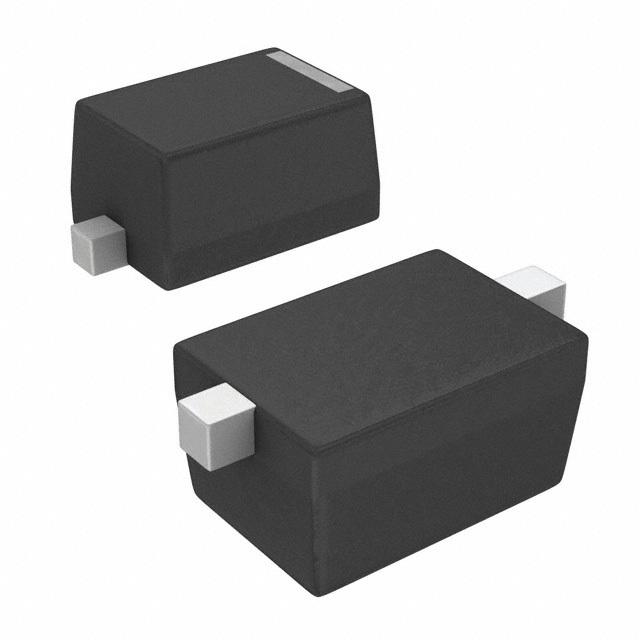
| 产品图片 |
|
| rohs | 符合RoHS无铅 / 符合限制有害物质指令(RoHS)规范要求 |
| 产品系列 | 二极管与整流器,整流器,STMicroelectronics STTH3R06- |
| 数据手册 | |
| 产品型号 | STTH3R06 |
| 不同If时的电压-正向(Vf) | 1.7V @ 3A |
| 不同 Vr、F时的电容 | - |
| 不同 Vr时的电流-反向漏电流 | 3µA @ 600V |
| 二极管类型 | 标准 |
| 产品 | Ultra Fast Recovery Rectifiers |
| 产品目录页面 | |
| 产品种类 | 整流器 |
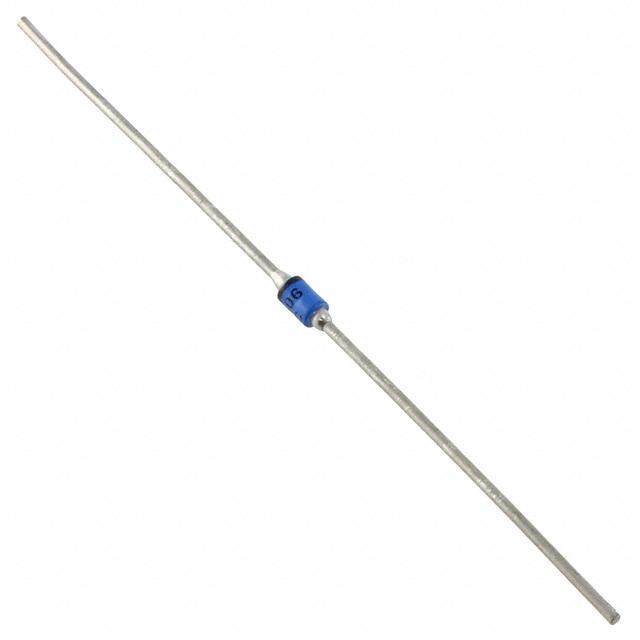
| 供应商器件封装 | DO-201AD |
| 其它名称 | 497-4414-3 |
| 其它有关文件 | http://www.st.com/web/catalog/sense_power/FM64/CL830/SC12/SS1654/PF78506?referrer=70071840 |
| 包装 | 带盒(TB) |
| 反向恢复时间(trr) | 35ns |
| 反向电压 | 600 V |
| 反向电流IR | 3 uA |
| 商标 | STMicroelectronics |
| 安装类型 | 通孔 |
| 安装风格 | Through Hole |
| 封装 | Ammo Pack |
| 封装/外壳 | DO-201AD,轴向 |
| 封装/箱体 | DO-201AD |
| 工作温度-结 | 175°C (最大) |
| 工厂包装数量 | 600 |
| 恢复时间 | 30 ns |
| 最大工作温度 | + 175 C |
| 最大浪涌电流 | 55 A |
| 最小工作温度 | - 65 C |
| 标准包装 | 600 |
| 正向电压下降 | 1.7 V |
| 正向连续电流 | 3 A |
| 热阻 | 75°C/W Ja |
| 电压-DC反向(Vr)(最大值) | 600V |
| 电流-平均整流(Io) | 3A |
| 系列 | STTH3R06 |
| 速度 | 快速恢复 =< 500 ns,> 200mA(Io) |
| 配置 | Single |


PDF Datasheet 数据手册内容提取
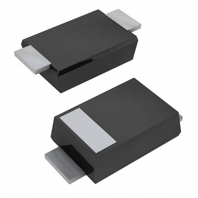
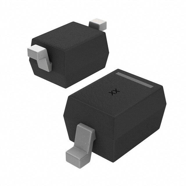
STTH3R06 ® TURBO 2 ULTRAFAST HIGH VOLTAGE RECTIFIER Table 1: Main Product Characteristics I 3 A F(AV) A K V 600 V RRM I (max) 100 µA R T 175°C j V (typ) 1.0 V F t (typ) 35 ns rr FEATURES AND BENEFITS DO-201AD ■ Ultrafast switching STTH3R06 ■ Low forward voltage drop ■ Low thermal resistance ■ Low leakage current (platinium doping) DESCRIPTION The STTH3R06, which is using ST Turbo 2 600V technology, is specially suited for use in switching SMB SMC power supplies, inverters and as a free wheeling STTH3R06U STTH3R06S diode. Table 2: Order Codes Part Number Marking STTH3R06 STTH3R06 STTH3R06RL STTH3R06 STTH3R06U 3R6U STTH3R06S R6S September 2005 REV. 3 1/9
STTH3R06 Table 3: Absolute Ratings (limiting values) Symbol Parameter Value Unit V Repetitive peak reverse voltage 600 V RRM I RMS forward current 10 A F(RMS) I Average forward current DO-201AD Tl = 80°C 3 A F(AV) δ = 0.5 SMB Tl = 55°C SMC Tl = 80°C I Surge non repetitive forward current DO-201AD tp = 10ms 55 A FSM SMB / SMC sinusoidal 45 T Storage temperature range -65 to + 175 °C stg T Maximum operating junction temperature 175 °C j Table 4: Thermal Parameters Symbol Parameter Maximum Unit R Junction to lead DO-201AD L = 10 mm 20 °C/W th(j-l) SMB 25 SMC 20 R Junction to ambient (see fig. 13) DO-201AD L = 10 mm 75 °C/W th(j-a) Table 5: Static Electrical Characteristics Symbol Parameter Test conditions Min. Typ Max. Unit I Reverse leakage current T = 25°C V = V 3 µA R j R RRM T = 150°C 15 100 j V Forward voltage drop T = 25°C I = 3A 1.7 V F j F T = 150°C 1.0 1.25 j 2 To evaluate the conduction losses use the following equation: P = 1.03 x IF(AV) + 0.09 IF (RMS) Table 6: Dynamic Characteristics Symbol Parameter Test conditions Min. Typ Max. Unit t Reverse recovery T = 25°C I = 0.5A I = 0.25A I = 1A 30 ns rr j F RR R time I = 1A dI /dt = -50 A/µs V =30V 35 F F R t Forward recovery T = 25°C I = 3A dI /dt = 100 A/µs 100 ns fr j F F time V = 1.1 x V FR Fmax V Forward recovery I = 3A dI /dt = 100 A/µs 10 V FP F F voltage 2/9
STTH3R06 Figure 1: Conduction losses versus average Figure 2: Forward voltage drop versus forward current current P(W) IFM(A) 5.0 50 δ= 0.1 δ= 0.2 δ= 0.5 4.5 δ= 0.05 45 Tj=150°C 4.0 δ= 1 40 (maximum values) 3.5 35 3.0 30 Tj=150°C (typical values) 2.5 25 Tj=25°C (maximum values) 2.0 20 1.5 T 15 1.0 10 0.5 IF(AV)(A) δ=tp/T tp 5 VFM(V) 0.0 0 0.0 0.5 1.0 1.5 2.0 2.5 3.0 3.5 4.0 0.0 0.5 1.0 1.5 2.0 2.5 3.0 3.5 4.0 Figure 3: Relative variation of thermal impedance Figure 4: Peak reverse recovery current junction ambient versus pulse duration (epoxy versus dI /dt (typical values) F printed circuit FR4, L = 10mm, S =1cm2) leads CU Zth(j-a)/Rth(j-a) IRM(A) 1.0 13 12 VR=400V 0.9 11 Tj=125°C IF=2 x IF(AV) 0.8 10 0.7 9 IF=IF(AV) 0.6 8 IF=0.5 x IF(AV) SMC 7 0.5 SCu= 1cm2 6 IF=0.25 x IF(AV) 0.4 SMB 5 0.3 SCu= 1cm2 4 DO-201AD 0.2 Single pulse Lleads= 10mm 3 2 0.1 tp(s) 1 dIF/dt(A/µs) 0.0 0 1.E-01 1.E+00 1.E+01 1.E+02 1.E+03 0 50 100 150 200 250 300 350 400 450 500 Figure 5: Reverse recovery time versus dI /dt Figure 6: Reverse recovery charges versus F (typical values) dI /dt (typical values) F trr(ns) Qrr(nC) 160 450 114500 VTjR==142050°CV 400 VTjR==142050°CV 130 350 IF=2 x IF(AV) 120 IF=2 x IF(AV) 110 300 100 90 IF=IF(AV) IF=0.5 x IF(AV) 250 IF=IF(AV) 80 70 200 60 IF=0.5 x IF(AV) 50 150 40 100 30 20 50 10 dIF/dt(A/µs) dIF/dt(A/µs) 0 0 0 50 100 150 200 250 300 350 400 450 500 0 50 100 150 200 250 300 350 400 450 500 3/9
STTH3R06 Figure 7: Softness factor versus d /dt (typical Figure 8: Relative variations of dynamic IF values) parameters versus junction temperature S factor 3.0 1.0 IF=IF(AV) 0.9 Sfactor 2.5 TVjR==142050°CV 0.8 IRM 0.7 2.0 0.6 QRR 0.5 1.5 0.4 1.0 0.3 0.2 VIFR==I4F0(A0VV) 0.5 0.1 Tj(°C) Reference:Tj=125°C dIF/dt(A/µs) 0.0 0.0 25 50 75 100 125 0 50 100 150 200 250 300 350 400 450 500 Figure 9: Transient peak forward voltage Figure 10: Forward recovery time versus dI /dt F versus dI /dt (typical values) (typical values) F VFP(V) tfr(ns) 20 200 18 ITFj==I1F2(A5V°)C 180 VFR=T1IFj.=1=1 Ix2F(5VA°VFC)max. 16 160 14 140 12 120 10 100 8 80 6 60 4 40 2 dIF/dt(A/µs) 20 dIF/dt(A/µs) 0 0 0 20 40 60 80 100 120 140 160 180 200 0 20 40 60 80 100 120 140 160 180 200 Figure 11: Junction capacitance versus Figure 12: Thermal resistance junction to reverse voltage applied (typical values) ambient versus copper surface under lead (epoxy FR4, e =35µm) (DO-201AD) CU C(pF) Rth(j-a)(°C/W) 100 80 F=1MHz VOSCT=j=3205m°CVRMS 70 60 DO-201AD 50 10 40 30 20 10 VR(V) SCU(cm²) 1 0 1 10 100 1000 0 1 2 3 4 5 6 7 8 9 10 4/9
STTH3R06 Figure 13: Thermal resistance junction to Figure 14: Thermal resistance versus lead ambient versus copper surface under lead length (epoxy FR4, e =35µm) (SMB / SMC) CU Rth(j-a)(°C/W) Rth(°C/W) 110 100 DO-201AD 100 90 90 80 Rth(j-a) 80 70 SMB 70 60 60 SMC 50 50 40 40 Rth(j-l) 30 30 20 20 10 SCU(cm²) 10 Llead(mm) 0 0 0.0 0.5 1.0 1.5 2.0 2.5 3.0 3.5 4.0 4.5 5.0 5 10 15 20 25 5/9
STTH3R06 Figure 15: SMB Package Mechanical Data DIMENSIONS REF. Millimeters Inches E1 Min. Max. Min. Max. A1 1.90 2.45 0.075 0.096 D A2 0.05 0.20 0.002 0.008 b 1.95 2.20 0.077 0.087 E c 0.15 0.41 0.006 0.016 E 5.10 5.60 0.201 0.220 A1 E1 4.05 4.60 0.159 0.181 C A2 D 3.30 3.95 0.130 0.156 L b L 0.75 1.60 0.030 0.063 Figure 16: SMB Foot Print Dimensions (in millimeters) 2.3 1.52 2.75 1.52 6/9
STTH3R06 Figure 17: SMC Package Mechanical Data DIMENSIONS REF. Millimeters Inches E1 Min. Max. Min. Max. A1 1.90 2.45 0.075 0.096 D A2 0.05 0.20 0.002 0.008 b 2.90 3.2 0.114 0.126 c 0.15 0.41 0.006 0.016 E E 7.75 8.15 0.305 0.321 A1 E1 6.60 7.15 0.260 0.281 C A2 E2 4.40 4.70 0.173 0.185 L b D 5.55 6.25 0.218 0.246 L 0.75 1.60 0.030 0.063 Figure 18: SMC Foot Print Dimensions (in millimeters) 3.3 2.0 4.2 2.0 7/9
STTH3R06 Figure 19: DO-201AD Package Mechanical Data DIMENSIONS B A B ØC REF. Millimeters Inches Min. Max. Min. Max. note 1 E E note 1 A 9.50 0.374 B 25.40 1.000 C 5.30 0.209 D 1.30 0.051 ØD ØD E 1.25 0.049 1 - The lead diameter ø D is not controlled over zone E note 2 2 - The minimum axial length within which the device NOTES may be placed with its leads bent at right angles is 0.59"(15 mm) In order to meet environmental requirements, ST offers these devices in ECOPACK® packages. These packages have a Lead-free second level interconnect . The category of second level interconnect is marked on the package and on the inner box label, in compliance with JEDEC Standard JESD97. The maximum ratings related to soldering conditions are also marked on the inner box label. ECOPACK is an ST trademark. ECOPACK specifications are available at: www.st.com. Table 7: Ordering Information Delivery Ordering type Marking Package Weight Base qty mode STTH3R06 STTH3R06 DO-201AD 1.12 g 600 Ammopack STTH3R06-RL STTH3R06 DO-201AD 1.12 g 1900 Tape & reel STTH3R06U 3R6U SMB 0.11 g 2500 Tape & reel STTH3R06S R6S SMC 0.243 g 2500 Tape & reel ■ Epoxy meets UL94, V0 ■ Band indicated cathode (DO-201AD) ■ Bending method: see application note AN1471 (DO-201AD) Table 8: Revision History Date Revision Description of Changes March-2003 1 First issue 07-Sep-2004 2 SMB and SMC packages added 14-Oct-2005 3 Changed marking of STTH3R06U from R06U to 3R6U on page 1. Added ECOPACK statement. 8/9
STTH3R06 Information furnished is believed to be accurate and reliable. However, STMicroelectronics assumes no responsibility for the consequences of use of such information nor for any infringement of patents or other rights of third parties which may result from its use. No license is granted by implication or otherwise under any patent or patent rights of STMicroelectronics. Specifications mentioned in this publication are subject to change without notice. This publication supersedes and replaces all information previously supplied. STMicroelectronics products are not authorized for use as critical components in life support devices or systems without express written approval of STMicroelectronics. The ST logo is a registered trademark of STMicroelectronics. All other names are the property of their respective owners © 2005 STMicroelectronics - All rights reserved STMicroelectronics group of companies Australia - Belgium - Brazil - Canada - China - Czech Republic - Finland - France - Germany - Hong Kong - India - Israel - Italy - Japan - Malaysia - Malta - Morocco - Singapore - Spain - Sweden - Switzerland - United Kingdom - United States of America www.st.com 9/9
Mouser Electronics Authorized Distributor Click to View Pricing, Inventory, Delivery & Lifecycle Information: S TMicroelectronics: STTH3R06 STTH3R06RL STTH3R06S STTH3R06U