ICGOO在线商城 > 分立半导体产品 > 二极管 - 整流器 - 单 > STPS3150RL
 Datasheet下载
- 型号: STPS3150RL
- 制造商: STMicroelectronics
- 库位|库存: xxxx|xxxx
- 要求:
| 数量阶梯 | 香港交货 | 国内含税 |
| +xxxx | $xxxx | ¥xxxx |
查看当月历史价格
查看今年历史价格
STPS3150RL产品简介:
ICGOO电子元器件商城为您提供STPS3150RL由STMicroelectronics设计生产,在icgoo商城现货销售,并且可以通过原厂、代理商等渠道进行代购。 STPS3150RL价格参考¥0.92-¥0.92。STMicroelectronicsSTPS3150RL封装/规格:二极管 - 整流器 - 单, 肖特基 通孔 二极管 150V 3A DO-201AD。您可以下载STPS3150RL参考资料、Datasheet数据手册功能说明书,资料中有STPS3150RL 详细功能的应用电路图电压和使用方法及教程。
STMicroelectronics的型号STPS3150RL是一款肖特基二极管,属于二极管 - 整流器 - 单类别。其主要应用场景包括以下几个方面:

 1. 电源管理
   - STPS3150RL适用于各种电源转换和整流电路中,例如开关电源(SMPS)中的同步整流或续流二极管。由于其低正向压降(典型值为0.35V),可以有效减少功率损耗,提高电源系统的效率。
   - 在直流-直流转换器中,该二极管可用于升压、降压或反激式拓扑结构中,提供高效的能量传递。

 2. 电池充电保护
   - 在便携式设备的电池充电电路中,STPS3150RL可以用作防反接保护二极管,防止电池电流倒流回充电器,同时降低电压降对充电效率的影响。

 3. 电机驱动
   - 在小型电机驱动电路中,该二极管可用作续流二极管(Flyback Diode),以吸收感性负载(如电机绕组)关断时产生的反电动势,保护开关器件(如MOSFET或BJT)免受过压损坏。

 4. 太阳能逆变器
   - 在光伏系统的小型逆变器中,STPS3150RL可作为旁路二极管使用,当某块太阳能电池板被遮挡或故障时,确保电流能够绕过问题组件继续流动,从而维持整个系统的正常运行。

 5. 通信设备
   - 在通信设备的电源模块中,该二极管可用于输入端的整流或输出端的保护,确保设备在宽电压范围下稳定工作。

 6. 消费电子
   - 该型号适合用于USB充电器、适配器等消费类电子产品中,提供高效整流功能,同时满足小型化设计需求。

 特性优势:
- 低正向压降:减少功耗和发热,提升系统效率。
- 高浪涌电流能力:能够承受瞬态大电流冲击,增强可靠性。
- 快速恢复时间:适合高频应用环境。

综上所述,STPS3150RL广泛应用于需要高效整流、低功耗及可靠性能的各种场景中,尤其适合中小功率的电子设备和系统。
| 参数 | 数值 |
| 产品目录 | |
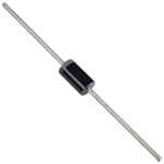
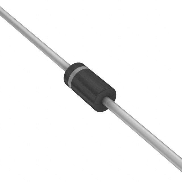
| 描述 | DIODE SCHOTTKY 150V 3A DO201AD肖特基二极管与整流器 3.0 Amp 150 Volt |
| 产品分类 | 单二极管/整流器分离式半导体 |
| 品牌 | STMicroelectronics |
| 产品手册 | |
| 产品图片 |
|
| rohs | 符合RoHS无铅 / 符合限制有害物质指令(RoHS)规范要求 |
| 产品系列 | 二极管与整流器,肖特基二极管与整流器,STMicroelectronics STPS3150RL- |
| 数据手册 | |
| 产品型号 | STPS3150RL |
| 不同If时的电压-正向(Vf) | 820mV @ 3A |
| 不同 Vr、F时的电容 | - |
| 不同 Vr时的电流-反向漏电流 | 2µA @ 150V |
| 二极管类型 | |
| 产品 | Schottky Rectifiers |
| 产品目录页面 | |
| 产品种类 | 肖特基二极管与整流器 |
| 供应商器件封装 | DO-201AD |
| 其它名称 | 497-3216-2 |
| 其它有关文件 | http://www.st.com/web/catalog/sense_power/FM64/CL1571/SC541/SS1619/PF70380?referrer=70071840 |
| 包装 | 带卷 (TR) |
| 反向恢复时间(trr) | - |
| 商标 | STMicroelectronics |
| 安装类型 | 通孔 |
| 安装风格 | Through Hole |
| 封装 | Reel |
| 封装/外壳 | DO-201AD,轴向 |
| 封装/箱体 | DO-201AD |
| 峰值反向电压 | 150 V |
| 工作温度-结 | 175°C (最大) |
| 工作温度范围 | + 175 C |
| 工具箱 | /product-detail/zh/497-8006A-KIT/497-8006A-KIT-ND/811052 |
| 工厂包装数量 | 1900 |
| 技术 | Silicon |
| 最大反向漏泄电流 | 2 uA |
| 最大工作温度 | + 175 C |
| 最大浪涌电流 | 150 A |
| 最小工作温度 | - 65 C |
| 标准包装 | 1,900 |
| 正向电压下降 | 0.89 V at 6 A |
| 正向连续电流 | 3 A |
| 热阻 | 15°C/W Jl |
| 电压-DC反向(Vr)(最大值) | 150V |
| 电流-平均整流(Io) | 3A |
| 系列 | STPS3150 |
| 速度 | 快速恢复 =< 500 ns,> 200mA(Io) |
| 配置 | Single |


- 商务部:美国ITC正式对集成电路等产品启动337调查
- 曝三星4nm工艺存在良率问题 高通将骁龙8 Gen1或转产台积电
- 太阳诱电将投资9.5亿元在常州建新厂生产MLCC 预计2023年完工
- 英特尔发布欧洲新工厂建设计划 深化IDM 2.0 战略
- 台积电先进制程称霸业界 有大客户加持明年业绩稳了
- 达到5530亿美元!SIA预计今年全球半导体销售额将创下新高
- 英特尔拟将自动驾驶子公司Mobileye上市 估值或超500亿美元
- 三星加码芯片和SET,合并消费电子和移动部门,撤换高东真等 CEO
- 三星电子宣布重大人事变动 还合并消费电子和移动部门
- 海关总署:前11个月进口集成电路产品价值2.52万亿元 增长14.8%


PDF Datasheet 数据手册内容提取
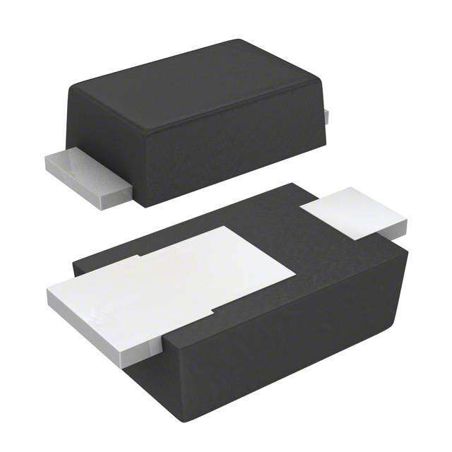
STPS3150 Power Schottky rectifier Datasheet - production data Description A 150 V Power Schottky rectifier are suited for switch mode power supplies on up to 24 V rails and high frequency converters. DO-201AD Packaged in Axial, SMB, and low-profile SMB, K this device is intended for use in consumer and computer applications like TV, STB, PC and DVD A A where low drop forward voltage is required to reduce power dissipation. K K SMB SMBflat Table 1. Device summary Symbol Value I 3 A F(AV) Features V 150 V RRM • Negligible switching losses T (max) 175 °C j • Low forward voltage drop for higher efficiency V (typ) 0.63 V F and extended battery life • Low thermal resistance • ECOPACK®2 compliant component August 2016 Doc ID 9474 Rev 6 1/9 This is information on a product in full production. www.st.com
Characteristics STPS3150 1 Characteristics Table 2. Absolute Ratings (limiting values at 25 °C unless otherwise specified) Symbol Parameter Value Unit VRRM Repetitive peak reverse voltage 150 V SMB T = 130 °C L Average forward current, IF(AV) δ= 0.5 square wave DO-201AD TL = 140 °C 3 A SMB flat T = 150 °C L SMB 80 Surge non repetitive IFSM forward current DO-201AD tp = 10 ms sinusoidal 100 A SMB flat 80 P (1) Repetitive peak avalanche power T = 125 °C, t = 10 µs 210 W ARM j p T Storage temperature range -65 to + 175 °C stg T Operating junction temperature(2) 175 °C j 1. For pulse time duration deratings, please refer to Figure3. More details regarding the avalanche energy measurements and diode validation in the avalanche are provided in the STMicroelectronics Application notes AN1768, “Admissible avalanche power of Schottky diodes” and AN2025, “Converter improvement using Schottky rectifier avalanche specification”. 2. d----dP---T--t--o-j---t<R-----t--h----(-1--j--–-----a----)- condition to avoid thermal runaway for a diode on its own heatsink Table 3. Thermal resistance Symbol Parameter Value Unit SMB flat 10 R Junction to lead SMB 20 °C/W th(j-l) Lead length = 10 mm DO-201AD 15 Table 4. Static electrical characteristics Symbol Parameter Tests conditions Min. Typ Max. Unit I (1) Reverse leakage Tj = 25 °C V = V 0.4 2.0 µA R current T = 125 °C R RRM 0.6 2.0 mA j T = 25 °C 0.78 0.82 j I = 3 A F T = 125 °C 0.63 0.67 V (2) Forward voltage drop j V F T = 25 °C 0.85 0.89 j I = 6 A F T = 125 °C 0.70 0.75 j 1. t = 5 ms, δ < 2% p 2. t = 380 µs, δ < 2% p To evaluate the conduction losses use the following equation: P = 0.59 x I + 0.027 I 2 F(AV) F (RMS) 2/9 Doc ID 9474 Rev 6
STPS3150 Characteristics Figure 1. A v erage forward power dissipation Figure 2. Average forward current versus versus average forward current ambient temperature (δ=0.5) PF(AV)(W) IF(AV)(A) 2.5 (cid:2)= 0.05 (cid:2)= 0.1 (cid:2)= 0.2 (cid:2)= 0.(cid:3) (cid:2)=1 3.5 Rth(j-a)=Rth(j-l) 3.0 2.0 SMB-Flat 2.5 DO-201AD 1.5 2.0 SMB 1.5 1.0 T 1.0 T 0.5 0.5 IF(AV)(A) (cid:2)=tp/T tp (cid:2)=tp/T tp Tamb(°C) 0.0 0.0 0.0 0.5 1.0 1.5 2.0 2.5 3.0 3.5 0 25 50 75 100 125 150 175 Figure 3. No r malized avalanche power derating Figure 4. Relative variation of thermal versus pulse duration impedance junction to ambient versus pulse duration (DO-201AD) PARM(tp) 1.0Zth(j-a)/Rth(j-a) 1 PARM(10 µs) DO-201AD 0.9 0.8 0.7 0.1 0.6 0.5 0.4 0.01 0.3 T 0.2 Single pulse 0.001 tp(µs) 0.1 tp(s) (cid:2)=tp/T tp 0.0 1 10 100 1000 1.E-01 1.E+00 1.E+01 1.E+02 1.E+03 Figure 5 . Relative variation of thermal Figure 6. Relative variation of thermal impedance junction to ambient versus pulse impedance junction to lead versus pulse duration (SMB) duration (SMBflat) Zth(j-a)/Rth(j-a) Zth(j-l)/Rth(j-l) 1.0 1.0 SMB SMBflat 0.9 0.9 0.8 0.8 0.7 0.7 0.6 0.6 0.5 0.5 0.4 0.4 0.3 0.3 T T 0.2 0.2 Single pulse Single pulse 0.1 tp(s) (cid:2)=tp/T tp 0.1 tp(s) (cid:2)=tp/T tp 0.0 0.0 1.E-02 1.E-01 1.E+00 1.E+01 1.E+02 1.E+03 1.E-04 1.E-03 1.E-02 1.E-01 1.E+00 1.E+01 Doc ID 9474 Rev 6 3/9 9
Characteristics STPS3150 Figure 7. Reverse leakage current versus Figure 8. Junction capacitance versus reverse reverse voltage applied (typical values) voltage applied (typical values) IR(µA) C(pF) 1.E+04 1000 F = 1MHZ Tj= 150 °C VOSC= 30 mVRMS 1.E+03 Tj= 25 °C Tj= 125 °C 1.E+02 Tj= 100 °C 1.E+01 Tj= 75 °C 100 Tj= 50 °C 1.E+00 Tj= 25 °C 1.E-01 VR(V) VR(V) 1.E-02 10 0 25 50 75 100 125 150 1 10 100 1000 Figure 9. Fo r ward voltage drop versus forward Figure 10. Thermal resistance junction to current ambient versus copper surface under each lead (typical values) R (°C/W) 100 IF(A) 200 th(j-a) (maTxjim= u1m25 v a°Clues) 180 epoxy printed boardFR4copper thickness = 35 µm SMB 160 Tj= 125 °C (typical values) 140 Tj= 25 °C (maximum values) 120 10 100 80 60 40 20 VF(V) 0 SCu(cm²) 1 0.0 0.2 0.4 0.6 0.8 1.0 1.2 1.4 1.6 1.8 0.0 0.5 1.0 1.5 2.0 2.5 3.0 3.5 4.0 4.5 5.0 Figure 11 . Thermal resistance junction to Figure 12. Thermal resistance versus lead ambient versus copper surface under each lead length (typical values) R (°C/W) 200 th(j-a) 90Rth(°C/W) 180 epoxy printed boardFR4copper thickness = 35 µm SMBflat DO-201AD 80 Rth(j-a) 160 70 140 60 120 50 100 40 80 60 30 Rth(j-l) 40 20 20 SCu(cm²) 10 Lleads(mm) 0 0 5 10 15 20 25 0.0 0.5 1.0 1.5 2.0 2.5 3.0 3.5 4.0 4.5 5.0 4/9 Doc ID 9474 Rev 6
STPS3150 Package information 2 Package information • Epoxy meets UL94, V0 • Lead-free package In order to meet environmental requirements, ST offers these devices in different grades of ECOPACK® packages, depending on their level of environmental compliance. ECOPACK® specifications, grade definitions and product status are available at: www.st.com. ECOPACK® is an ST trademark. Figure 13. SMB dimensions (definitions) E1 D E A1 C A2 L b Table 5. SMB dimensions (values) Dimensions Ref. Millimeters Inches Min. Max. Min. Max. A1 1.90 2.45 0.075 0.096 A2 0.05 0.20 0.002 0.008 b 1.95 2.20 0.077 0.087 c 0.15 0.40 0.006 0.016 E 5.10 5.60 0.201 0.220 E1 4.05 4.60 0.159 0.181 D 3.30 3.95 0.130 0.156 L 0.75 1.50 0.030 0.059 Figure 14. SMB footprint (dimensions in mm) 1.62 2.60 1.62 (0.064) (0.102) (0.064) 2.18 (0.086) 5.84 (0.23) Doc ID 9474 Rev 6 5/9 9
Package information STPS3150 Figure 15. SMBflat dimensions (definitions) A c D L 2x L2 2x E E1 L L1 2x b Table 6. SMBflat dimensions (values) Dimensions Ref. Millimeters Inches Min. Typ. Max. Min. Typ. Max. A 0.90 1.10 0.035 0.043 b(1) 1.95 2.20 0.077 0.087 c(1) 0.15 0.40 0.006 0.016 D 3.30 3.95 0.130 0.156 E 5.10 5.60 0.200 0.220 E1 4.05 4.60 0.189 0.181 L 0.75 1.50 0.029 0.059 L1 0.40 0.016 L2 0.60 0.024 1. Applies to plated leads Figure 16. SMB Flat footprint 5.84 (0.230) 2.07 (0.082) 1.20 3.44 1.20 (0.047) (0.136) (0.047) millimeters (inches) 6/9 Doc ID 9474 Rev 6
STPS3150 Package information Figure 17. DO-201AD dimensions (definitions) B A B E E Note 1 Note 1 ØD Note 2 ØC Table 7. DO-201AD dimensions (values) Dimensions Ref. Millimeters Inches Min. Max. Min. Max. A 9.50 0.374 B 25.40 1.000 C 5.30 0.209 D(1) 1.30 0.051 E 1.25 0.049 Note 2(2) 15 0.59 1. The lead diameter D is not controlled over zone E 2. The minimum length, which must stay straight between the right angles after bending, is 15 mm (0.59”) Doc ID 9474 Rev 6 7/9 9
Ordering information STPS3150 3 Ordering information Table 8. Ordering information Order code Marking Package Weight Base qty Delivery mode STPS3150U G315 SMB 107 mg 2500 Tape and reel STPS3150UF FG315 SMB flat 50 mg 5000 Tape and reel STPS3150 STPS3150 DO-201AD 1.12 g 600 Ammopack STPS3150RL STPS3150 DO-201AD 1.12 g 1900 Tape and reel 4 Revision history Table 9. Document revision history Date Revision Changes May-2003 2A Last update. Reformatted to current standard. Added ECOPACK statement. 31-May-2006 3 Updated SMB footprint in Figure 12. Changed nF to pF in Figure 8. 08-Feb-2007 4 Added SMB flat and SMB flat e package. 20-Jul-2011 5 Updated Table 2. 11-Aug-2016 6 Updated Table2 and all curves. 8/9 Doc ID 9474 Rev 6
STPS3150 IMPORTANT NOTICE – PLEASE READ CAREFULLY STMicroelectronics NV and its subsidiaries (“ST”) reserve the right to make changes, corrections, enhancements, modifications, and improvements to ST products and/or to this document at any time without notice. Purchasers should obtain the latest relevant information on ST products before placing orders. ST products are sold pursuant to ST’s terms and conditions of sale in place at the time of order acknowledgement. Purchasers are solely responsible for the choice, selection, and use of ST products and ST assumes no liability for application assistance or the design of Purchasers’ products. No license, express or implied, to any intellectual property right is granted by ST herein. Resale of ST products with provisions different from the information set forth herein shall void any warranty granted by ST for such product. ST and the ST logo are trademarks of ST. All other product or service names are the property of their respective owners. Information in this document supersedes and replaces information previously supplied in any prior versions of this document. © 2016 STMicroelectronics – All rights reserved Doc ID 9474 Rev 6 9/9 9
Mouser Electronics Authorized Distributor Click to View Pricing, Inventory, Delivery & Lifecycle Information: S TMicroelectronics: STPS3150U STPS3150 STPS3150RL STPS3150UF