ICGOO在线商城 > 集成电路(IC) > PMIC - 监控器 > STM706TM6F
 Datasheet下载
- 型号: STM706TM6F
- 制造商: STMicroelectronics
- 库位|库存: xxxx|xxxx
- 要求:
| 数量阶梯 | 香港交货 | 国内含税 |
| +xxxx | $xxxx | ¥xxxx |
查看当月历史价格
查看今年历史价格
STM706TM6F产品简介:
ICGOO电子元器件商城为您提供STM706TM6F由STMicroelectronics设计生产,在icgoo商城现货销售,并且可以通过原厂、代理商等渠道进行代购。 STM706TM6F价格参考¥2.54-¥2.54。STMicroelectronicsSTM706TM6F封装/规格:PMIC - 监控器, Supervisor Push-Pull, Totem Pole 1 Channel 8-SO。您可以下载STM706TM6F参考资料、Datasheet数据手册功能说明书,资料中有STM706TM6F 详细功能的应用电路图电压和使用方法及教程。
STMicroelectronics(意法半导体)的STM706TM6F是一款属于PMIC监控器类别的集成电路,主要用于系统电源管理和复位控制。该器件集成了上电复位、掉电警告和看门狗定时器功能,适用于需要高可靠性和稳定运行的嵌入式系统。

典型应用场景包括工业控制设备、通信设备、消费类电子产品及家用电器等。在单片机(MCU)或微处理器系统中,STM706TM6F可确保电源上电时提供可靠的复位信号,防止因电压不稳定导致的误操作或程序跑飞。当系统电压下降至预设阈值以下时,其电压监控功能会及时触发复位,保护系统数据完整性。

此外,集成的看门狗定时器可在程序陷入死循环或异常停滞时自动复位系统,提升设备的自恢复能力。该芯片采用SOT-23-6小型封装,体积小巧,功耗低,非常适合空间受限且对稳定性要求较高的便携式设备或长期运行的工业模块。

综上,STM706TM6F广泛应用于需可靠复位与电源监控的电子系统中,是保障系统稳定启动和持续运行的关键元件。
| 参数 | 数值 |
| 产品目录 | 集成电路 (IC)半导体 |
| 描述 | SUPERVISOR 3V WATCHDOG 8SOIC监控电路 4.38V Reset Suprvsr |
| 产品分类 | |
| 品牌 | STMicroelectronics |
| 产品手册 | |
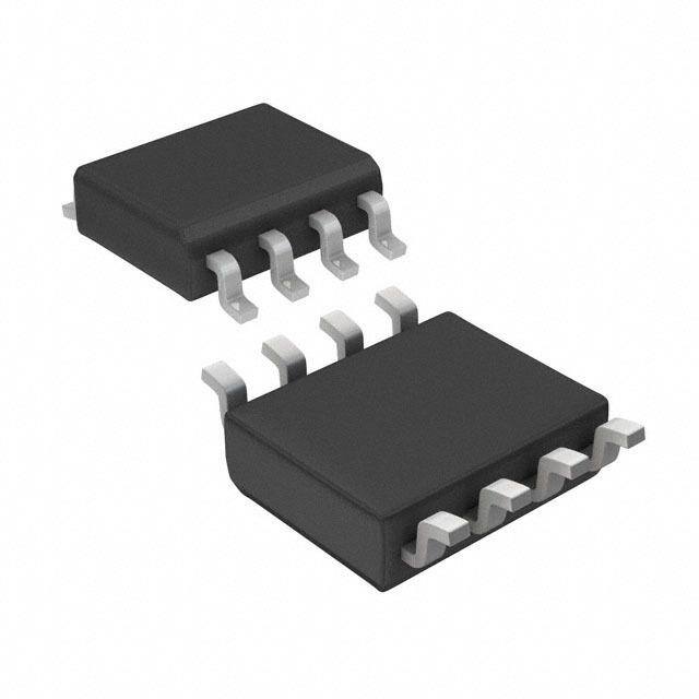
| 产品图片 |
|
| rohs | 符合RoHS无铅 / 符合限制有害物质指令(RoHS)规范要求 |
| 产品系列 | 电源管理 IC,监控电路,STMicroelectronics STM706TM6F- |
| NumberofInputsMonitored | 1 Input |
| 数据手册 | |
| 产品型号 | STM706TM6F |
| 产品培训模块 | http://www.digikey.cn/PTM/IndividualPTM.page?site=cn&lang=zhs&ptm=30015 |
| 产品目录页面 | |
| 产品种类 | 监控电路 |
| 人工复位 | Manual Reset |
| 供应商器件封装 | 8-SO |
| 其它名称 | 497-3839-6 |
| 其它有关文件 | http://www.st.com/web/catalog/sense_power/FM1946/SC792/PF86458?referrer=70071840 |
| 功率失效检测 | Yes |
| 包装 | Digi-Reel® |
| 受监控电压数 | 1 |
| 商标 | STMicroelectronics |
| 复位 | 低有效 |
| 复位超时 | 最小为 140 ms |
| 安装类型 | 表面贴装 |
| 安装风格 | SMD/SMT |
| 封装 | Reel |
| 封装/外壳 | 8-SOIC(0.154",3.90mm 宽) |
| 封装/箱体 | SO-8 |
| 工作温度 | -40°C ~ 85°C |
| 工作电源电流 | 40 uA |
| 工厂包装数量 | 2500 |
| 最大功率耗散 | 320 mW |
| 最大工作温度 | + 85 C |
| 最小工作温度 | - 40 C |
| 标准包装 | 1 |
| 欠电压阈值 | 3 V |
| 电压-阈值 | 3.08V |
| 电池备用开关 | No Backup |
| 电源电压-最大 | 5.5 V |
| 电源电压-最小 | 1 V |
| 监视器 | Watchdog |
| 类型 | Voltage Supervisory |
| 系列 | STM706T |
| 芯片启用信号 | No Chip Enable |
| 被监测输入数 | 1 Input |
| 输出 | 推挽式,图腾柱 |
| 输出类型 | Active Low, Push-Pull |
| 过电压阈值 | 3.15 V |
| 阈值电压 | 3 V |


- 商务部:美国ITC正式对集成电路等产品启动337调查
- 曝三星4nm工艺存在良率问题 高通将骁龙8 Gen1或转产台积电
- 太阳诱电将投资9.5亿元在常州建新厂生产MLCC 预计2023年完工
- 英特尔发布欧洲新工厂建设计划 深化IDM 2.0 战略
- 台积电先进制程称霸业界 有大客户加持明年业绩稳了
- 达到5530亿美元!SIA预计今年全球半导体销售额将创下新高
- 英特尔拟将自动驾驶子公司Mobileye上市 估值或超500亿美元
- 三星加码芯片和SET,合并消费电子和移动部门,撤换高东真等 CEO
- 三星电子宣布重大人事变动 还合并消费电子和移动部门
- 海关总署:前11个月进口集成电路产品价值2.52万亿元 增长14.8%


PDF Datasheet 数据手册内容提取
STM706T/S/R, STM706P, STM708T/S/R 3 V supervisor Datasheet - production data Features • Precision V monitor CC – T: 3.00 V ≤ V ≤ 3.15 V RST – S: 2.88 V ≤ V ≤ 3.00 V RST – R: STM706P: 2.59 V ≤ V ≤ 2.70 V RST (cid:27) • RST and RST outputs • 200 ms (typ.) t rec (cid:20) • Watchdog timer - 1.6 s (typ.) (cid:54)(cid:50)(cid:27)(cid:3)(cid:11)(cid:48)(cid:12) • Manual reset input (MR) • Power-fail comparator (PFI/PFO) • Low supply current - 40 µA (typ.) • Guaranteed RST (RST) assertion down to V = 1.0 V CC • Operating temperature: –40 °C to 85 °C (industrial grade) (cid:55)(cid:54)(cid:54)(cid:50)(cid:51)(cid:27)(cid:3)(cid:22)(cid:91)(cid:22)(cid:3)(cid:11)(cid:39)(cid:54)(cid:12) • RoHS compliance (cid:38)(cid:82)(cid:81)(cid:87)(cid:68)(cid:70)(cid:87)(cid:3)(cid:79)(cid:82)(cid:70)(cid:68)(cid:79)(cid:3)(cid:54)(cid:55)(cid:3)(cid:86)(cid:68)(cid:79)(cid:72)(cid:86)(cid:3)(cid:82)(cid:73)(cid:73)(cid:76)(cid:70)(cid:72)(cid:3)(cid:73)(cid:82)(cid:85)(cid:3)(cid:68)(cid:89)(cid:68)(cid:76)(cid:79)(cid:68)(cid:69)(cid:76)(cid:79)(cid:76)(cid:87)(cid:92) – Lead-free components are compliant with the RoHS directive Applications • Computers • Controllers • Intelligent instruments Table 1. Device summary Watchdog Watchdog Active low Active high Manual Power-fail input output(1) RST (1) RST(1) reset input comparator STM706T/S/R ✓ ✓ ✓ ✓ ✓ STM706P(2) ✓ ✓ ✓ ✓ ✓ STM708T/S/R ✓ ✓ ✓ ✓ 1. Push-pull output. 2. The STM706P device is identical to the STM706R device, except its reset output is active high. December 2015 DocID10518 Rev 13 1/32 This is information on a product in full production. www.st.com
Contents STM706T/S/R, STM706P, STM708T/S/R Contents 1 Description . . . . . . . . . . . . . . . . . . . . . . . . . . . . . . . . . . . . . . . . . . . . . . . . . 5 2 Pin descriptions . . . . . . . . . . . . . . . . . . . . . . . . . . . . . . . . . . . . . . . . . . . . 8 2.1 MR . . . . . . . . . . . . . . . . . . . . . . . . . . . . . . . . . . . . . . . . . . . . . . . . . . . . . . . 8 2.2 WDI . . . . . . . . . . . . . . . . . . . . . . . . . . . . . . . . . . . . . . . . . . . . . . . . . . . . . . 8 2.3 WDO . . . . . . . . . . . . . . . . . . . . . . . . . . . . . . . . . . . . . . . . . . . . . . . . . . . . . . 8 2.4 RST . . . . . . . . . . . . . . . . . . . . . . . . . . . . . . . . . . . . . . . . . . . . . . . . . . . . . . 8 2.5 RST . . . . . . . . . . . . . . . . . . . . . . . . . . . . . . . . . . . . . . . . . . . . . . . . . . . . . . 8 2.6 PFI . . . . . . . . . . . . . . . . . . . . . . . . . . . . . . . . . . . . . . . . . . . . . . . . . . . . . . . 8 2.7 PFO . . . . . . . . . . . . . . . . . . . . . . . . . . . . . . . . . . . . . . . . . . . . . . . . . . . . . . 9 3 Operation . . . . . . . . . . . . . . . . . . . . . . . . . . . . . . . . . . . . . . . . . . . . . . . . . 11 3.1 Reset output . . . . . . . . . . . . . . . . . . . . . . . . . . . . . . . . . . . . . . . . . . . . . . . .11 3.2 Push-button reset input . . . . . . . . . . . . . . . . . . . . . . . . . . . . . . . . . . . . . . .11 3.3 Watchdog input (STM706T/S/R and STM706P) . . . . . . . . . . . . . . . . . . . .11 3.4 Watchdog output (STM706T/S/R and STM706P) . . . . . . . . . . . . . . . . . . .11 3.5 Power-fail input/output . . . . . . . . . . . . . . . . . . . . . . . . . . . . . . . . . . . . . . . 12 3.6 Ensuring a valid reset output down to V = 0 V . . . . . . . . . . . . . . . . . . . 12 CC 3.7 Interfacing to microprocessors with bi-directional reset pins . . . . . . . . . . 13 4 Typical operating characteristics . . . . . . . . . . . . . . . . . . . . . . . . . . . . . 14 5 Maximum ratings . . . . . . . . . . . . . . . . . . . . . . . . . . . . . . . . . . . . . . . . . . . 21 6 DC and AC parameters . . . . . . . . . . . . . . . . . . . . . . . . . . . . . . . . . . . . . . 22 7 Package information . . . . . . . . . . . . . . . . . . . . . . . . . . . . . . . . . . . . . . . . 26 7.1 SO8 package information . . . . . . . . . . . . . . . . . . . . . . . . . . . . . . . . . . . . . 27 7.2 TSSOP8 3x3 (DS) package information . . . . . . . . . . . . . . . . . . . . . . . . . . 28 8 Part numbering . . . . . . . . . . . . . . . . . . . . . . . . . . . . . . . . . . . . . . . . . . . . 29 9 Revision history . . . . . . . . . . . . . . . . . . . . . . . . . . . . . . . . . . . . . . . . . . . 31 2/32 DocID10518 Rev 13
STM706T/S/R, STM706P, STM708T/S/R List of tables List of tables Table 1. Device summary. . . . . . . . . . . . . . . . . . . . . . . . . . . . . . . . . . . . . . . . . . . . . . . . . . . . . . . . . . 1 Table 2. Signal names . . . . . . . . . . . . . . . . . . . . . . . . . . . . . . . . . . . . . . . . . . . . . . . . . . . . . . . . . . . . 6 Table 3. Pin description . . . . . . . . . . . . . . . . . . . . . . . . . . . . . . . . . . . . . . . . . . . . . . . . . . . . . . . . . . . 9 Table 4. Absolute maximum ratings. . . . . . . . . . . . . . . . . . . . . . . . . . . . . . . . . . . . . . . . . . . . . . . . . 21 Table 5. Operating and AC measurement conditions. . . . . . . . . . . . . . . . . . . . . . . . . . . . . . . . . . . . 22 Table 6. DC and AC characteristics . . . . . . . . . . . . . . . . . . . . . . . . . . . . . . . . . . . . . . . . . . . . . . . . . 24 Table 7. SO8 - 8-lead plastic small outline, 150 mils body width, mechanical data . . . . . . . . . . . . . 27 Table 8. TSSOP8 - 8-lead, thin shrink small outline, 3 x 3 mm body size, mechanical data . . . . . . . . . . . . . . . . . . . . . . . . . . . . . . . . . . . . . . . . . . . . . . . . . . . . . . . . . 28 Table 9. Ordering information scheme. . . . . . . . . . . . . . . . . . . . . . . . . . . . . . . . . . . . . . . . . . . . . . . 29 Table 10. Marking description. . . . . . . . . . . . . . . . . . . . . . . . . . . . . . . . . . . . . . . . . . . . . . . . . . . . . . . 30 Table 11. Document revision history . . . . . . . . . . . . . . . . . . . . . . . . . . . . . . . . . . . . . . . . . . . . . . . . . 31 DocID10518 Rev 13 3/32 3
List of figures STM706T/S/R, STM706P, STM708T/S/R List of figures Figure 1. Logic diagram (STM706T/S/R and STM706P). . . . . . . . . . . . . . . . . . . . . . . . . . . . . . . . . . . 5 Figure 2. Logic diagram (STM708T/S/R). . . . . . . . . . . . . . . . . . . . . . . . . . . . . . . . . . . . . . . . . . . . . . . 5 Figure 3. STM706T/S/R and STM706P SO8 connections. . . . . . . . . . . . . . . . . . . . . . . . . . . . . . . . . . 6 Figure 4. STM706T/S/R and STM706P TSSOP8 connections . . . . . . . . . . . . . . . . . . . . . . . . . . . . . . 6 Figure 5. STM708T/S/R SO8 connections . . . . . . . . . . . . . . . . . . . . . . . . . . . . . . . . . . . . . . . . . . . . . 6 Figure 6. STM708T/S/R TSSOP8 connections . . . . . . . . . . . . . . . . . . . . . . . . . . . . . . . . . . . . . . . . . . 7 Figure 7. Block diagram (STM706T/S/R and STM706P). . . . . . . . . . . . . . . . . . . . . . . . . . . . . . . . . . . 9 Figure 8. Block diagram (STM708T/S/R). . . . . . . . . . . . . . . . . . . . . . . . . . . . . . . . . . . . . . . . . . . . . . 10 Figure 9. Hardware hookup. . . . . . . . . . . . . . . . . . . . . . . . . . . . . . . . . . . . . . . . . . . . . . . . . . . . . . . . 10 Figure 10. Reset output valid to ground circuit . . . . . . . . . . . . . . . . . . . . . . . . . . . . . . . . . . . . . . . . . . 12 Figure 11. Interfacing to microprocessors with bi-directional reset I/O . . . . . . . . . . . . . . . . . . . . . . . . 13 Figure 12. Supply current vs. temperature (no load). . . . . . . . . . . . . . . . . . . . . . . . . . . . . . . . . . . . . . 14 Figure 13. V threshold vs. temperature. . . . . . . . . . . . . . . . . . . . . . . . . . . . . . . . . . . . . . . . . . . . . . 15 PFI Figure 14. Reset comparator propagation delay vs. temperature . . . . . . . . . . . . . . . . . . . . . . . . . . . . 15 Figure 15. Power-up t vs. temperature . . . . . . . . . . . . . . . . . . . . . . . . . . . . . . . . . . . . . . . . . . . . . . 16 rec Figure 16. Normalized reset threshold vs. temperature . . . . . . . . . . . . . . . . . . . . . . . . . . . . . . . . . . . 16 Figure 17. Watchdog timeout period vs. temperature . . . . . . . . . . . . . . . . . . . . . . . . . . . . . . . . . . . . . 17 Figure 18. PFI to PFO propagation delay vs. temperature . . . . . . . . . . . . . . . . . . . . . . . . . . . . . . . . . 17 Figure 19. Output voltage vs. load current (V = 5 V; T = 25 °C) . . . . . . . . . . . . . . . . . . . . . . . . . . 18 CC A Figure 20. RST output voltage vs. supply voltage. . . . . . . . . . . . . . . . . . . . . . . . . . . . . . . . . . . . . . . . 18 Figure 21. RST output voltage vs. supply voltage. . . . . . . . . . . . . . . . . . . . . . . . . . . . . . . . . . . . . . . . 19 Figure 22. Power-fail comparator response time (assertion). . . . . . . . . . . . . . . . . . . . . . . . . . . . . . . . 19 Figure 23. Power-fail comparator response time (de-assertion) . . . . . . . . . . . . . . . . . . . . . . . . . . . . . 20 Figure 24. Maximum transient duration vs. reset threshold overdrive. . . . . . . . . . . . . . . . . . . . . . . . . 20 Figure 25. AC testing input/output waveforms . . . . . . . . . . . . . . . . . . . . . . . . . . . . . . . . . . . . . . . . . . 22 Figure 26. Power-fail comparator waveform . . . . . . . . . . . . . . . . . . . . . . . . . . . . . . . . . . . . . . . . . . . . 22 Figure 27. MR timing waveform. . . . . . . . . . . . . . . . . . . . . . . . . . . . . . . . . . . . . . . . . . . . . . . . . . . . . . 23 Figure 28. Watchdog timing (STM706T/S/R and STM706P) . . . . . . . . . . . . . . . . . . . . . . . . . . . . . . . 23 Figure 29. SO8 - 8-lead plastic small outline, 150 mils body width, package outline. . . . . . . . . . . . . . 27 Figure 30. TSSOP8 - 8-lead, thin shrink small outline, 3 x 3 mm body size, package outline. . . . . . . 28 4/32 DocID10518 Rev 13
STM706T/S/R, STM706P, STM708T/S/R Description 1 Description The STM70x supervisors are self-contained devices which provide microprocessor supervisory functions. A precision voltage reference and comparator monitors the V input CC for an out-of-tolerance condition. When an invalid V condition occurs, the reset output CC (RST) is forced low (or high in the case of RST). These devices also offer a watchdog timer (except for STM708T/S/R) as well as a power-fail comparator to provide the system with an early warning of impending power failure. The STM706P device is identical to the STM706R device, except its reset output is active high. These devices are available in a standard 8-pin SOIC package or a space-saving 8- pin TSSOP package. Figure 1. Logic diagram (STM706T/S/R and STM706P) VCC WDI WDO STM706T/S/R, (1) MR STM706P RST (RST) PFI PFO VSS AI08841 1. For STM706P only. Figure 2. Logic diagram (STM708T/S/R) VCC RST MR STM708T/S/R RST PFI PFO VSS AI08842 DocID10518 Rev 13 5/32 31
Description STM706T/S/R, STM706P, STM708T/S/R Table 2. Signal names Symbol Name MR Push-button reset input WDI Watchdog input WDO Watchdog output RST Active low reset output RST(1) Active high reset output V Supply voltage CC PFI Power-fail input PFO Power-fail output V Ground SS NC No connect 1. For STM706P and STM708T/S/R only. Figure 3. STM706T/S/R and STM706P SO8 connections SO8 MR 1 8 WDO VCC 2 7 RST(RST)(1) VSS 3 6 WDI PFI 4 5 PFO AI08837 1. For STM706P reset output is active high. Figure 4. STM706T/S/R and STM706P TSSOP8 connections TSSOP8 (1) RST(RST) 1 8 WDI WDO 2 7 PFO MR 3 6 PFI VCC 4 5 VSS AI08838 1. For STM706P reset output is active high. Figure 5. STM708T/S/R SO8 connections SO8 MR 1 8 RST VCC 2 7 RST VSS 3 6 NC PFI 4 5 PFO AI08839 6/32 DocID10518 Rev 13
STM706T/S/R, STM706P, STM708T/S/R Description Figure 6. STM708T/S/R TSSOP8 connections TSSOP8 RST 1 8 NC RST 2 7 PFO MR 3 6 PFI VCC 4 5 VSS AI08840 DocID10518 Rev 13 7/32 31
Pin descriptions STM706T/S/R, STM706P, STM708T/S/R 2 Pin descriptions 2.1 MR A logic low on MR asserts the reset output. Reset remains asserted as long as MR is low and for t after MR returns high. This active low input has an internal pull-up. It can be rec driven from a TTL or CMOS logic line, or shorted to ground with a switch. Leave open if unused. 2.2 WDI If WDI remains high or low for 1.6 s, the internal watchdog timer runs out and reset (or WDO) is triggered. The internal watchdog timer clears while reset is asserted or when WDI sees a rising or falling edge. The watchdog function can be disabled by allowing the WDI pin to float. This feature is available for the “D” version only (see Section 8: Part numbering). 2.3 WDO WDO goes low when a transition does not occur on WDI within 1.6 s, and remains low until a transition occurs on WDI (indicating the watchdog interrupt has been serviced) or MR input is asserted (goes low). WDO also goes low when V falls below the reset threshold; CC however, unlike the reset output, WDO goes high as soon as V exceeds the reset CC threshold. Output type is push-pull. Note: For those devices with a WDO output, a watchdog timeout will not trigger reset unless WDO is connected to MR. 2.4 RST Pulses low for t when triggered, and stays low whenever V is below the reset rec CC threshold or when MR is a logic low. It remains low for t after either V rises above the rec CC reset threshold, the watchdog triggers a reset, or MR goes from low to high. 2.5 RST Pulses high for t when triggered, and stays high whenever V is above the reset rec CC threshold or when MR is a logic high. It remains high for t after either V falls below the rec CC reset threshold, the watchdog triggers a reset, or MR goes from high to low. 2.6 PFI When PFI is less than V , PFO goes low; otherwise, PFO remains high. Connect to PFI ground if unused. 8/32 DocID10518 Rev 13
STM706T/S/R, STM706P, STM708T/S/R Pin descriptions 2.7 PFO When PFI is less than V , PFO goes low; otherwise, PFO remains high. Output type is PFI push-pull. PFO pin is not supposed to be forced low by a processor. MR input is gated off during the period PFO is forced low. Leave open if unused. Table 3. Pin description Pin STM706P STM706T/S/R STM708T/S/R Name Function SO8 TSSOP8 SO8 TSSOP8 SO8 TSSOP8 1 3 1 3 1 3 MR Push-button reset input 6 8 6 8 — — WDI Watchdog input 8 2 8 2 — — WDO Watchdog output (push-pull) — — 7 1 7 1 RST Active low reset output 7 1 — — 8 2 RST Active high reset output 2 4 2 4 2 4 V Supply voltage CC 4 6 4 6 4 6 PFI Power-fail input 5 7 5 7 5 7 PFO Power-fail output (push-pull) 3 5 3 5 3 5 V Ground SS — — — — 6 8 NC No connect Figure 7. Block diagram (STM706T/S/R and STM706P) WDI WATCHDOG WDI transitional TIMER WDO detector VCC VRST COMPARE VCC trec (1) MR generator RST (RST) PFI VPFI COMPARE PFO AI08829 1. For STM706P only DocID10518 Rev 13 9/32 31
Pin descriptions STM706T/S/R, STM706P, STM708T/S/R Figure 8. Block diagram (STM708T/S/R) V CC V COMPARE RST RST V CC trec MR generator RST PFI V COMPARE PFO PFI AI08830 Figure 9. Hardware hookup Regulator Unregulated voltage VIN VCC VCC STM706T/S/R; 0.1 μF STM706P; STM708T/S/R (1) (1) WDI WDO To microprocessor IRQ R1 From microprocessor PFI PFO To microprocessor NMI R2 MR RST Push-button To microprocessor reset (2) RST AI08843 1. For STM706T/S/R and STM706P devices 2. For STM706P and STM708T/S/R devices 10/32 DocID10518 Rev 13
STM706T/S/R, STM706P, STM708T/S/R Operation 3 Operation 3.1 Reset output The STM70x supervisor asserts a reset signal to the MCU whenever V goes below the CC reset threshold (V ), a watchdog timeout occurs (if WDO is connected to MR), or when the RST push-button reset input (MR) is taken low. RST is guaranteed to be a logic low (logic high for STM706P and STM708T/S/R) for V < V down to V =1 V for T = 0 °C to 85 °C. CC RST CC A During power-up, once V exceeds the reset threshold an internal timer keeps RST low for CC the reset timeout period, t . After this interval RST returns high. rec If V drops below the reset threshold, RST goes low. Each time RST is asserted, it stays CC low for at least the reset timeout period (t ). Any time V goes below the reset threshold rec CC the internal timer clears. The reset timer starts when V returns above the reset threshold. CC 3.2 Push-button reset input A logic low on MR asserts reset. Reset remains asserted while MR is low, and for t (see rec Figure 27) after it returns high. The MR input has an internal 40 kΩ pull-up resistor, allowing it to be left open if not used. This input can be driven with TTL/CMOS-logic levels or with open-drain / collector outputs. Connect a normally open momentary switch from MR to GND to create a manual reset function; external debounce circuitry is not required. If MR is driven from long cables or the device is used in a noisy environment, connect a 0.1 µF capacitor from MR to GND to provide additional noise immunity. MR may float, or be tied to V when CC not used. 3.3 Watchdog input (STM706T/S/R and STM706P) The watchdog timer can be used to detect an out-of-control MCU. If the MCU does not toggle the watchdog input (WDI) within t (1.6 s), the watchdog output pin (WDO) is WD asserted. The internal 1.6s timer is cleared by either: 1. a reset pulse, or 2. by toggling WDI (high-to-low or low-to-high), which can detect pulses as short as 50 ns. See Figure 28 for STM706T/S/R and STM706P. The timer remains cleared and does not count for as long as reset is asserted. As soon as reset is released, the timer starts counting. Note: The watchdog function may be disabled by floating WDI or tri-stating the driver connected to WDI. When tri-stated or disconnected, the maximum allowable leakage current is 10 µA and the maximum allowable load capacitance is 200 pF. 3.4 Watchdog output (STM706T/S/R and STM706P) When V drops below the reset threshold, WDO will go low even if the watchdog timer has CC not yet timed out. However, unlike the reset output, WDO goes high as soon as V CC exceeds the reset threshold. WDO may be used to generate a reset pulse by connecting it to the MR input. DocID10518 Rev 13 11/32 31
Operation STM706T/S/R, STM706P, STM708T/S/R 3.5 Power-fail input/output The power-fail input (PFI) is compared to an internal reference voltage (independent from the V comparator). If PFI is less than the power-fail threshold (V ), the power-fail RST PFI output (PFO) will go low. This function is intended for use as an undervoltage detector to signal a failing power supply. Typically PFI is connected through an external voltage divider (see Figure 9) to either the unregulated DC input (if it is available) or the regulated output of the V regulator. The voltage divider can be set up such that the voltage at PFI falls below CC V several milliseconds before the regulated V input to the STM70x or the micro- PFI CC processor drops below the minimum operating voltage. If the comparator is unused, PFI should be connected to V and PFO left unconnected. SS PFO may be connected to MR on the STM70x so that a low voltage on PFI will generate a reset output. 3.6 Ensuring a valid reset output down to V = 0 V CC When V falls below 1 V, the state of the RST output can no longer be guaranteed, and CC becomes essentially an open circuit. If a high value pulldown resistor is added to the RST pin, the output will be held low during this condition. A resistor value of approximately 100 kΩ will be large enough to not load the output under operating conditions, but still sufficient to pull RST to ground during this low voltage condition (see Figure 10). Figure 10. Reset output valid to ground circuit STM70x RST R1 AI08844 12/32 DocID10518 Rev 13
STM706T/S/R, STM706P, STM708T/S/R Operation 3.7 Interfacing to microprocessors with bi-directional reset pins Microprocessors with bi-directional reset pins can contend with the STM70x reset output. For example, if the reset output is driven high and the micro wants to pull it low, signal contention will result. To prevent this from occurring, connect a 4.7kΩ resistor between the reset output and the micro's reset I/O as in Figure 11. Figure 11. Interfacing to microprocessors with bi-directional reset I/O Buffered reset to other system components VCC VCC STM70x Microprocessor 4.7 kΩ RST RST GND GND AI08845 DocID10518 Rev 13 13/32 31
Typical operating characteristics STM706T/S/R, STM706P, STM708T/S/R 4 Typical operating characteristics Typical values are at T = 25 °C. A Figure 12. Supply current vs. temperature (no load) 30 25 20 A) µ ent ( 15 urr c y VCC = 2.7 V uppl 10 VCC = 3.0 V S VCC = 3.6 V VCC = 4.5 V VCC = 5.5 V 5 0 –40 –20 0 20 40 60 80 100 120 Temperature (°C) AI09141b 14/32 DocID10518 Rev 13
STM706T/S/R, STM706P, STM708T/S/R Typical operating characteristics Figure 13. V threshold vs. temperature PFI 1.270 1.265 1.260 VCC = 2.5 V VCC = 3.0 V VCC = 3.3 V V) 1.255 VCC = 3.6 V d ( ol 1.250 h s e hr 1.245 t FI P 1.240 V 1.235 1.230 1.225 –40 –20 0 20 40 60 80 100 120 Temperature (°C) AI09142b Figure 14. Reset comparator propagation delay vs. temperature 30 28 26 24 s) µ y ( 22 a el d n 20 o ati ag 18 p o Pr 16 14 12 10 –40 –20 0 20 40 60 80 100 120 Temperature (°C) AI09143b DocID10518 Rev 13 15/32 31
Typical operating characteristics STM706T/S/R, STM706P, STM708T/S/R Figure 15. Power-up t vs. temperature rec 240 235 230 VCC = 3.0 V s) (mc 225 VCC = 4.5 V e tr VCC = 5.5 V 220 215 210 –40 –20 0 20 40 60 80 100 120 Temperature (°C) AI09144b Figure 16. Normalized reset threshold vs. temperature 1.004 d 1.002 ol h s e hr t et s 1.000 e r d e z ali m or 0.998 N 0.996 –40 –20 0 20 40 60 80 100 120 Temperature (°C) AI09145b 16/32 DocID10518 Rev 13
STM706T/S/R, STM706P, STM708T/S/R Typical operating characteristics Figure 17. Watchdog timeout period vs. temperature 1.90 1.85 s) od ( 1.80 eri p ut o 1.75 e m ti og VCC = 3.0 V hd 1.70 VCC = 4.5 V c at VCC = 5.5 V W 1.65 1.60 –40 –20 0 20 40 60 80 100 120 Temperature (˚C) AI09146b Figure 18. PFI to PFO propagation delay vs. temperature 4.0 VCC = 3.0 V VCC = 3.6 V 3.0 VCC = 4.5 V a el d VCC = 5.5 V n o gati 2.0 a p o pr O F P o 1.0 FI t P 0.0 –40 –20 0 20 40 60 80 100 120 Temperature (˚C) AI09148b DocID10518 Rev 13 17/32 31
Typical operating characteristics STM706T/S/R, STM706P, STM708T/S/R Figure 19. Output voltage vs. load current (V = 5 V; T = 25 °C) CC A 5.00 4.98 V) ( T U O V 4.96 4.94 0 10 20 30 40 50 IOUT (mA) AI10496 Figure 20. RST output voltage vs. supply voltage 5 5 VRST VCC 4 4 3 3 V) (ST VCC (V) R 2 2 V 1 1 0 0 500 ms / div AI09149b 18/32 DocID10518 Rev 13
STM706T/S/R, STM706P, STM708T/S/R Typical operating characteristics Figure 21. RST output voltage vs. supply voltage 5 5 VRST VCC 4 4 V) 3 3 (T VCC (V) S R V 2 2 1 1 0 0 500 ms / div AI09150b Figure 22. Power-fail comparator response time (assertion) (cid:24)(cid:57) (cid:51)(cid:41)(cid:50) (cid:20)(cid:57)(cid:18) (cid:71)(cid:76)(cid:89) (cid:19)(cid:57) (cid:20)(cid:17)(cid:22)(cid:57) (cid:51)(cid:41)(cid:44) (cid:24)(cid:19)(cid:19)(cid:80)(cid:57)(cid:18)(cid:71)(cid:76)(cid:89) (cid:19)(cid:57) (cid:24)(cid:19)(cid:19)(cid:81)(cid:86)(cid:18)(cid:71)(cid:76)(cid:89) DocID10518 Rev 13 19/32 31
Typical operating characteristics STM706T/S/R, STM706P, STM708T/S/R Figure 23. Power-fail comparator response time (de-assertion) (cid:24)(cid:57) (cid:51)(cid:41)(cid:50) (cid:20)(cid:57)(cid:18) (cid:71)(cid:76)(cid:89) (cid:19)(cid:57) (cid:20)(cid:17)(cid:22)(cid:57) (cid:51)(cid:41)(cid:44) (cid:24)(cid:19)(cid:19)(cid:80)(cid:57)(cid:18)(cid:71)(cid:76)(cid:89) (cid:19)(cid:57) (cid:24)(cid:19)(cid:19)(cid:81)(cid:86)(cid:18)(cid:71)(cid:76)(cid:89) Figure 24. Maximum transient duration vs. reset threshold overdrive 6000 5000 s) n (µ 4000 o Reset occurs urati above the curve d 3000 nt e si n a Tr 2000 1000 0 0.001 0.01 0.1 1 10 Reset comparator overdrive, VRST – VCC (V) AI09156b 20/32 DocID10518 Rev 13
STM706T/S/R, STM706P, STM708T/S/R Maximum ratings 5 Maximum ratings Stressing the device above the rating listed in the Table 4: Absolute maximum ratings may cause permanent damage to the device. These are stress ratings only and operation of the device at these or any other conditions above those indicated in Table 5: Operating and AC measurement conditions of this specification is not implied. Exposure to absolute maximum rating conditions for extended periods may affect device reliability. Table 4. Absolute maximum ratings Symbol Parameter Value Unit T Storage temperature (V off) –55 to 150 °C STG CC T (1) Lead solder temperature for 10 seconds 260 °C SLD V (2) Input or output voltage –0.3 to V +0.3 V IO CC V Supply voltage –0.3 to 7.0 V CC I Output current 20 mA O P Power dissipation 320 mW D 1. Reflow at peak temperature of 260 °C. The time above 255 °C must not exceed 30 seconds. 2. Negative undershoot of –1.5 V for up to 10 ns or positive overshoot of V + 1.5 V for up to 10 ns is CC allowable on the WDI and MR input pins. DocID10518 Rev 13 21/32 31
DC and AC parameters STM706T/S/R, STM706P, STM708T/S/R 6 DC and AC parameters This section summarizes the operating measurement conditions, and the DC and AC characteristics of the device. The parameters in Table 6: DC and AC characteristics are derived from tests performed under the measurement conditions summarized in Table 5: Operating and AC measurement conditions. Designers should check that the operating conditions in their circuit match the operating conditions when relying on the quoted parameters. Table 5. Operating and AC measurement conditions Parameter STM70x Unit V supply voltage 1.0 to 5.5 V CC Ambient operating temperature (T ) –40 to 85 °C A Input rise and fall times ≤ 5 ns Input pulse voltages 0.2 to 0.8 V V CC Input and output timing ref. voltages 0.3 to 0.7 V V CC Figure 25. AC testing input/output waveforms 0.8 VCC 0.7 VCC 0.3 VCC 0.2 V CC AI02568 Figure 26. Power-fail comparator waveform VCC VRST trec PFO RST AI08860a 22/32 DocID10518 Rev 13
STM706T/S/R, STM706P, STM708T/S/R DC and AC parameters Figure 27. MR timing waveform MR tMLRL (1) RST tMLMH trec AI07837a 1. RST for STM706P and STM708T/S/R. Figure 28. Watchdog timing (STM706T/S/R and STM706P) VCC RST trec WDI tWD WDO AI08833 DocID10518 Rev 13 23/32 31
DC and AC parameters STM706T/S/R, STM706P, STM708T/S/R Table 6. DC and AC characteristics Symbol Description Test condition(1) Min. Typ. Max. Unit V Operating voltage 1.2(2) 5.5 V CC V < 3.6 V 35 50 µA CC I V supply current CC CC V < 5.5 V 40 60 µA CC Input leakage current 0 V < V < V –1 +1 µA (WDI) IN CC Input leakage current (WDI) with watchdog 0 V < V < V -110 110 µA disable feature (“D” IN CC I version) LI Input leakage current 0 V < V < V –25 2 +25 nA (PFI) IN CC V (max.) < V < 3.6 V 25 80 250 µA Input leakage current RST CC (MR) 4.5 V < V < 5.5 V 75 125 300 µA CC 4.5 V < V < 5.5 V 2.0 V CC V Input high voltage (MR) IH V (max.) < V < 3.6 V 0.7 V V RST CC CC V Input high voltage (WDI) V (max.) < V < 5.5 V 0.7 V V IH RST CC CC 4.5 V < V < 5.5 V 0.8 V CC V Input low voltage (MR) IL V (max.) < V < 3.6 V 0.6 V RST CC V Input low voltage (WDI) V (max.) < V < 5.5 V 0.3 V V IL RST CC CC Output low voltage (PFO, V = V (max.), V CC RST 0.3 V OL RST, RST, WDO) I = 3.2 mA SINK I = 50 µA, V = 1.0 V, SINK CC 0.3 V T = 0 °C to 85 °C A V Output low voltage (RST) OL I = 100 µA, SINK 0.3 V V = 1.2 V CC Output high voltage (RST, I = 1 mA, V SOURCE 2.4 V OH RST, WDO) V = V (max.) CC RST Output high voltage I = 75 µA, SOURCE 0.8 V V (PFO) V = V (max.) CC CC RST Power-fail comparator PFI falling V PFI input threshold (STM70xP/R, V = 3.0 V; 1.20 1.25 1.30 V PFI CC STM70xS/T, V = 3.3 V) CC PFI to PFO propagation t 2 µs PFD delay 24/32 DocID10518 Rev 13
STM706T/S/R, STM706P, STM708T/S/R DC and AC parameters Table 6. DC and AC characteristics (continued) Symbol Description Test condition(1) Min. Typ. Max. Unit Reset thresholds STM706P/70xR 2.55 2.63 2.70 V V Reset threshold(3) STM70xS 2.85 2.93 3.00 V RST STM70xT 3.00 3.08 3.15 V Reset threshold 20 mV hysteresis Blank (see Table 9) 140 200 280 t RST pulse width ms rec A(4) (see Table 9) 160 200 280 Push-button reset input tMLMH MR pulse width VRST (max.) < VCC < 3.6 V 500 ns (or tMR) 4.5 V < VCC < 5.5 V 150 ns tMLRL MR to RST output delay VRST (max.) < VCC < 3.6 V 750 ns (or tMRD) 4.5 V < VCC < 5.5 V 250 ns Watchdog timer (STM706T/S/R and STM706P) STM706P/70xR, 1.12 1.60 2.24 s V = 3.0 V CC t Watchdog timeout period WD STM70xS/70XT, V = 3.3 V CC 4.5 V < V < 5.5 V 50 ns CC WDI pulse width V (max.) < V < 3.6 V 100 ns RST CC 1. Valid for ambient operating temperature: T = –40 to 85 °C; V = V (max.) to 5.5 V (except where noted). A CC RST 2. V (min) = 1.0 V for T = 0 °C to +85 °C. CC A 3. For V falling. CC 4. STM706P/STM70xR device, V = 3 V; STM706xS/STM70xT device, V = 3.3 V. CC CC DocID10518 Rev 13 25/32 31
Package information STM706T/S/R, STM706P, STM708T/S/R 7 Package information In order to meet environmental requirements, ST offers these devices in different grades of ECOPACK® packages, depending on their level of environmental compliance. ECOPACK® specifications, grade definitions and product status are available at: www.st.com. ECOPACK® is an ST trademark. 26/32 DocID10518 Rev 13
STM706T/S/R, STM706P, STM708T/S/R Package information 7.1 SO8 package information Figure 29. SO8 - 8-lead plastic small outline, 150 mils body width, package outline A2 A C B ddd e D 8 E H 1 A1 L SO-A Note: Drawing is not to scale. Table 7. SO8 - 8-lead plastic small outline, 150 mils body width, mechanical data Dimensions Symbol mm inches Typ. Min. Max. Typ. Min. Max. A — 1.35 1.75 — 0.053 0.069 A1 — 0.10 0.25 — 0.004 0.010 B — 0.33 0.51 — 0.013 0.020 C — 0.19 0.25 — 0.007 0.010 D — 4.80 5.00 — 0.189 0.197 ddd — — 0.10 — — 0.004 E — 3.80 4.00 — 0.150 0.157 e 1.27 — — 0.050 — — H — 5.80 6.20 — 0.228 0.244 h — 0.25 0.50 — 0.010 0.020 L — 0.40 0.90 — 0.016 0.035 α — 0° 8° — 0° 8° N 8 8 DocID10518 Rev 13 27/32 31
Package information STM706T/S/R, STM706P, STM708T/S/R 7.2 TSSOP8 3x3 (DS) package information Figure 30. TSSOP8 - 8-lead, thin shrink small outline, 3 x 3 mm body size, package outline D 8 5 c E1 E 1 4 A1 L A A2 CP L1 b e TSSOP8BM Note: Drawing is not to scale. Table 8. TSSOP8 - 8-lead, thin shrink small outline, 3 x 3 mm body size, mechanical data Dimensions Symbol mm inches Typ. Min. Max. Typ. Min. Max. A — — 1.10 — — 0.043 A1 — 0.05 0.15 — 0.002 0.006 A2 0.85 0.75 0.95 0.034 0.030 0.037 b — 0.25 0.40 — 0.010 0.016 c — 0.13 0.23 — 0.005 0.009 CP — — 0.10 — — 0.004 D 3.00 2.90 3.10 0.118 0.114 0.122 e 0.65 — — 0.026 — — E 4.90 4.65 5.15 0.193 0.183 0.203 E1 3.00 2.90 3.10 0.118 0.114 0.122 L 0.55 0.40 0.70 0.022 0.016 0.030 L1 0.95 — — 0.037 — — α — 0° 6° — 0° 6° N 8 8 28/32 DocID10518 Rev 13
STM706T/S/R, STM706P, STM708T/S/R Part numbering 8 Part numbering Table 9. Ordering information scheme Example: STM706 T D M 6 F Device type STM706 STM708 Reset threshold voltage T: 3.00 V ≤ V ≤ 3.15 V RST S: 2.88 V ≤ V ≤ 3.00 V RST R: STM706P: 2.59 V ≤ V ≤ 2.70 V RST Watchdog disable Blank = not activated D = activated RST pulse width Blank = 140 to 280 ms A(1) = 160 to 280 ms Package M = SO8 DS(2) = TSSOP8 Temperature range 6 = –40 to 85 °C Shipping method F = ECOPACK® packages, tape and reel 1. Available in SO8 (M) package only 2. Contact local ST sales office for availability For other options, or for more information on any aspect of this device, please contact the ST sales office nearest you. DocID10518 Rev 13 29/32 31
Part numbering STM706T/S/R, STM706P, STM708T/S/R Table 10. Marking description Part number Reset threshold Package Topside marking SO8 STM706P 2.63 V 706P TSSOP8 SO8 STM706T 3.08 V 706T TSSOP8 SO8 STM706S 2.93 V 706S TSSOP8 SO8 STM706R 2.63 V 706R TSSOP8 SO8 STM706RD 2.63 V 706RD TSSOP8 SO8 STM708T 3.08 V 708T TSSOP8 SO8 STM708S 2.93 V 708S TSSOP8 SO8 STM708R 2.63 V 708R TSSOP8 30/32 DocID10518 Rev 13
STM706T/S/R, STM706P, STM708T/S/R Revision history 9 Revision history Table 11. Document revision history Date Revision Changes Oct-2003 1 Initial release. Reformatted; update characteristics (Figure 2, 3, 8 to 10, 27 to 29; 12-Dec-2003 2 Table 6 to 9). 16-Jan-2004 2.1 Add Typical operating characteristics (Figure 13, to 19, 21, to 25). 09-Apr-2004 3 Reformatted; update characteristics (Figure 15, 19, 21, 22, 25; Table 8). 25-May-2004 4 Update characteristics (Table 3, Table 6). 02-Jul-2004 5 Datasheet promoted; waveform corrected (Table 27). 21-Sep-2004 6 Clarify root part numbers; (Figure 2, to 10, 29; Table 1, 3, 6, 9). 25-Feb-2005 7 Update typical characteristics (Figure 13 to 25). Updated Table 1, Table 3, Table 4, Table 6, Table 9, Section 2.3, 02-Nov-2009 8 Section 2.7, text in Section 7; reformatted document. Updated Table 4, corrected typo in Table 2, Section 2.3, Section 3, 30-Apr-2010 9 Section 5 and Section 6, Figure 17, Table 7 and Table 8. 06-Aug-2010 10 Updated Features, Section 4: Typical operating characteristics; Table 9. Updated Section 2.7, Section 5 and Disclaimer, minor typo 06-Sep-2011 11 modifications throughout the document. Added Applications, updated Section 2.2 and Section 2.3, added note 21-Aug-2012 12 to Section 3.3, added cross-references in Section 5 and Section 6, minor text corrections throughout document. Updated layout of cover page and Section 7: Package information. Added information about the watchdog disable function to Section 2.2: 15-Dec-2015 13 WDI, Table 6, Table 9, and Table 10. Table 9: removed the “E” option (tubes) from shipping method DocID10518 Rev 13 31/32 31
STM706T/S/R, STM706P, STM708T/S/R IMPORTANT NOTICE – PLEASE READ CAREFULLY STMicroelectronics NV and its subsidiaries (“ST”) reserve the right to make changes, corrections, enhancements, modifications, and improvements to ST products and/or to this document at any time without notice. Purchasers should obtain the latest relevant information on ST products before placing orders. ST products are sold pursuant to ST’s terms and conditions of sale in place at the time of order acknowledgement. Purchasers are solely responsible for the choice, selection, and use of ST products and ST assumes no liability for application assistance or the design of Purchasers’ products. No license, express or implied, to any intellectual property right is granted by ST herein. Resale of ST products with provisions different from the information set forth herein shall void any warranty granted by ST for such product. ST and the ST logo are trademarks of ST. All other product or service names are the property of their respective owners. Information in this document supersedes and replaces information previously supplied in any prior versions of this document. © 2015 STMicroelectronics – All rights reserved 32/32 DocID10518 Rev 13
Mouser Electronics Authorized Distributor Click to View Pricing, Inventory, Delivery & Lifecycle Information: S TMicroelectronics: STM708SM6F STM706SM6F STM706RM6F STM708RM6F STM706TM6F STM706PM6F STM708TM6F STM706PM6E STM706RDS6F STM706RM6E STM706SM6E STM706TM6E STM708RM6E STM708SDS6F STM708SM6E STM708TDS6F STM708TM6E STM706PAM6F STM706RAM6F STM706TAM6F STM708SAM6F STM708TAM6F STM706TDS6F STM706RDS6E STM706RDAM6F