ICGOO在线商城 > 集成电路(IC) > PMIC - 监控器 > ADM1086AKSZ-REEL7
 Datasheet下载
- 型号: ADM1086AKSZ-REEL7
- 制造商: Analog
- 库位|库存: xxxx|xxxx
- 要求:
| 数量阶梯 | 香港交货 | 国内含税 |
| +xxxx | $xxxx | ¥xxxx |
查看当月历史价格
查看今年历史价格
ADM1086AKSZ-REEL7产品简介:
ICGOO电子元器件商城为您提供ADM1086AKSZ-REEL7由Analog设计生产,在icgoo商城现货销售,并且可以通过原厂、代理商等渠道进行代购。 ADM1086AKSZ-REEL7价格参考。AnalogADM1086AKSZ-REEL7封装/规格:PMIC - 监控器, 推挽式,图腾柱 监控器 1 通道 SC-70-6。您可以下载ADM1086AKSZ-REEL7参考资料、Datasheet数据手册功能说明书,资料中有ADM1086AKSZ-REEL7 详细功能的应用电路图电压和使用方法及教程。
Analog Devices Inc.(ADI公司)的ADM1086AKSZ-REEL7是一款PMIC(电源管理集成电路)监控器,广泛应用于需要精确电压和电流监控的系统中。该器件的主要应用场景包括但不限于以下几个方面:

 1. 服务器与数据中心
在服务器和数据中心的应用中,电源管理和监控至关重要。ADM1086AKSZ-REEL7可以用于监控服务器主板上的各种电源轨,确保每个电源轨的电压和电流都在安全范围内。它能够实时检测电源异常,并通过报警或关断功能防止硬件损坏。此外,它还可以帮助优化电源效率,降低能耗。

 2. 通信设备
通信设备如路由器、交换机等对电源的稳定性和可靠性要求极高。ADM1086AKSZ-REEL7可以在这些设备中监控电源状态,确保设备在高温、高负载等恶劣环境下仍能正常工作。它还可以用于多路电源系统的冗余设计,确保当一路电源失效时,其他电源能够及时接管,保证系统的持续运行。

 3. 工业自动化
在工业自动化领域,特别是PLC(可编程逻辑控制器)、HMI(人机界面)等设备中,电源监控是保障系统稳定性的关键。ADM1086AKSZ-REEL7可以监控这些设备中的多个电源轨,确保所有模块都能获得稳定的电源供应。它还可以用于故障诊断,帮助工程师快速定位电源问题,减少停机时间。

 4. 医疗设备
医疗设备如监护仪、超声设备等对电源的精度和稳定性有极高的要求。ADM1086AKSZ-REEL7可以用于监控这些设备中的电源模块,确保设备在长时间运行过程中不会因为电源波动而出现误操作或数据丢失。它的高精度监控能力还可以帮助提高设备的安全性,确保患者的生命体征监测数据准确无误。

 5. 汽车电子
在汽车电子系统中,特别是在新能源汽车中,电池管理系统(BMS)和车载充电器等模块需要精确的电源监控。ADM1086AKSZ-REEL7可以用于监控这些模块中的电源状态,确保电池充放电过程中的安全性,并提供过压、过流保护功能,延长电池寿命。

总之,ADM1086AKSZ-REEL7凭借其高精度、多功能的特点,适用于多种对电源监控要求严格的场景,能够有效提升系统的可靠性和安全性。
| 参数 | 数值 |
| 产品目录 | 集成电路 (IC)半导体 |
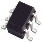
| 描述 | IC SIMPLE SEQUENCER P-P SC70-6监控电路 VTG Seq w/ Active Hi Push-Pull Enable Out |
| 产品分类 | |
| 品牌 | Analog Devices Inc |
| 产品手册 | |
| 产品图片 |
|
| rohs | 符合RoHS无铅 / 符合限制有害物质指令(RoHS)规范要求 |
| 产品系列 | 电源管理 IC,监控电路,Analog Devices ADM1086AKSZ-REEL7Simple Sequencers® |
| NumberofInputsMonitored | 1 Input |
| 数据手册 | |
| 产品型号 | ADM1086AKSZ-REEL7 |
| 产品目录页面 | |
| 产品种类 | 监控电路 |
| 人工复位 | No Manual Reset |
| 供应商器件封装 | SC-70-6 |
| 其它名称 | ADM1086AKSZ-REEL7CT |
| 包装 | 剪切带 (CT) |
| 受监控电压数 | 1 |
| 商标 | Analog Devices |
| 复位 | 高有效 |
| 复位超时 | 可调节/可选择 |
| 安装类型 | 表面贴装 |
| 安装风格 | SMD/SMT |
| 封装 | Reel |
| 封装/外壳 | 6-TSSOP,SC-88,SOT-363 |
| 封装/箱体 | SC-70-6 |
| 工作温度 | -40°C ~ 85°C |
| 工作电源电流 | 10 uA |
| 工厂包装数量 | 3000 |
| 最大工作温度 | + 125 C |
| 最小工作温度 | - 40 C |
| 标准包装 | 1 |
| 欠电压阈值 | 0.56 V |
| 电压-阈值 | 可调节/可选择 |
| 电池备用开关 | Backup |
| 电源电压-最大 | 3.6 V |
| 电源电压-最小 | 2.25 V |
| 监视器 | No Watchdog |
| 类型 | 序列发生器 |
| 系列 | ADM1086 |
| 芯片启用信号 | Chip Enable |
| 被监测输入数 | 1 Input |
| 输出 | 推挽式,图腾柱 |
| 输出类型 | Open Drain, Push-Pull |
| 过电压阈值 | 0.64 V |
| 阈值电压 | 0.6 V |


- 商务部:美国ITC正式对集成电路等产品启动337调查
- 曝三星4nm工艺存在良率问题 高通将骁龙8 Gen1或转产台积电
- 太阳诱电将投资9.5亿元在常州建新厂生产MLCC 预计2023年完工
- 英特尔发布欧洲新工厂建设计划 深化IDM 2.0 战略
- 台积电先进制程称霸业界 有大客户加持明年业绩稳了
- 达到5530亿美元!SIA预计今年全球半导体销售额将创下新高
- 英特尔拟将自动驾驶子公司Mobileye上市 估值或超500亿美元
- 三星加码芯片和SET,合并消费电子和移动部门,撤换高东真等 CEO
- 三星电子宣布重大人事变动 还合并消费电子和移动部门
- 海关总署:前11个月进口集成电路产品价值2.52万亿元 增长14.8%


PDF Datasheet 数据手册内容提取
Simple Sequencers® in 6-Lead SC70 Data Sheet ADM1085/ADM1086/ADM1087 FEATURES FUNCTIONAL BLOCK DIAGRAMS Provide programmable time delays between enable signals VCC Can be cascaded with power modules for multiple ADM1085/ADM1086 supply sequencing Power supply monitoring from 0.6 V VIN CAPACITOR ADJUSTABLE Output stages 0.6V DELAY ENOUT High voltage (up to 22 V) open-drain output (ADM1085/ADM1087) Push-pull output (ADM1086) Capacitor-adjustable time delays GND CEXT ENIN High voltage (up to 22 V) enable and V inputs IN Low power consumption (15 μA) VCC Specified over –40°C to +125°C temperature range ADM1087 6-lead SC70 package VIN CAPACITOR ADJUSTABLE APPLICATIONS 0.6V DELAY ENOUT Desktop/notebook computers, servers LRoowut peorsw er portable equipment GND CEXT ENIN 04591-001 Base stations Figure 1. Line cards Graphics cards GENERAL DESCRIPTION The ADM1085/ADM1086/ADM1087 are simple sequencing All four models have a dedicated enable input pin that allows circuits that provide a time delay between the enabling of the output signal to the regulator to be controlled externally. voltage regulators and/or dc-dc converters at power-up in This is an active high input (ENIN) for the ADM1085 and multiple supply systems. When the output voltage of the first ADM1086, and an active low input (ENIN) for the ADM1087. power module reaches a preset threshold, a time delay is initiated before an enable signal allows subsequent regulators to The Simple Sequencers are specified over the extended power up. Any number of these devices can be cascaded with −40°C to +125°C temperature range. With low current regulators to allow sequencing of multiple power supplies. consumption of 15 μA (typical) and 6-lead SC70 packaging, the parts are suitable for low-power portable applications. Threshold levels can be set with a pair of external resistors in a Table 1. Selection Table voltage divider configuration. With appropriate resistor values, Output Stage the threshold can be adjusted to monitor voltages as low as 0.6 V. Part No. Enable Input ENOUT ENOUT The ADM1086 has a push-pull output stage, with active high ADM1085 ENIN Open-drain (ENOUT). The ADM1085 has an active-high (ENOUT) logic ADM1086 ENIN Push-pull output; the ADM1087 has an active-low (ENOUT) output. Both the ADM1085 and ADM1087 have open-drain output stages ADM1087 ENIN Open-drain that can be pulled up to voltage levels as high as 22 V through an external resistor. This level-shifting property ensures compatibility with enable input logic levels of different regulators and converters. Rev. B Document Feedback Information furnished by Analog Devices is believed to be accurate and reliable. However, no responsibility is assumed by Analog Devices for its use, nor for any infringements of patents or other One Technology Way, P.O. Box 9106, Norwood, MA 02062-9106, U.S.A. rights of third parties that may result from its use. Specifications subject to change without notice. No license is granted by implication or otherwise under any patent or patent rights of Analog Devices. Tel: 781.329.4700 ©2004–2014 Analog Devices, Inc. All rights reserved. Trademarks and registered trademarks are the property of their respective owners. Technical Support www.analog.com
ADM1085/ADM1086/ADM1087 Data Sheet TABLE OF CONTENTS Features .............................................................................................. 1 Capacitor-Adjustable Delay Circuit ............................................9 Applications ....................................................................................... 1 Open-Drain and Push-Pull Outputs ....................................... 10 Functional Block Diagrams ............................................................. 1 Application Information ................................................................ 11 General Description ......................................................................... 1 Sequencing Circuits ................................................................... 11 Revision History ............................................................................... 2 Dual LOFO Sequencing ............................................................ 13 Specifications ..................................................................................... 3 Simultaneous Enabling .............................................................. 13 Absolute Maximum Ratings ............................................................ 4 Power Good Signal Delays ........................................................ 13 ESD Caution .................................................................................. 4 Quad-Supply Power Good Indicator ....................................... 14 Pin Configuration and Function Descriptions ............................. 5 Sequencing with FET Switches ................................................. 14 Typical Performance Characteristics ............................................. 6 Outline Dimensions ....................................................................... 15 Circuit Information .......................................................................... 9 Ordering Guide .......................................................................... 15 Timing Characteristics and Truth Tables .................................. 9 REVISION HISTORY 5/14—Rev. A to Rev. B Removed ADM1088 ...................................................... Throughout Changes to Capacitor-Adjustable Delay Circuit........................... 9 Removed Figure 26; Renumbered Sequentially.......................... 12 Changes to Ordering Guide .......................................................... 15 4/06—Rev. 0 to Rev. A Added Lead-Free Models .................................................. Universal Update Outline Dimensions ......................................................... 15 Changes to Ordering Guide .......................................................... 15 7/04—Revision 0: Initial Version Rev. B | Page 2 of 16
Data Sheet ADM1085/ADM1086/ADM1087 SPECIFICATIONS V = full operating range, T = −40°C to +125°C, unless otherwise noted. CC A Table 2. Parameter Min Typ Max Unit Test Conditions/Comments SUPPLY V Operating Voltage Range 2.25 3.6 V CC V Operating Voltage Range 0 22 V IN Supply Current 10 15 μA V Rising Threshold, V 0.56 0.6 0.64 V V = 3.3 V IN TH_RISING CC V Falling Threshold, V 0.545 0.585 0.625 V V = 3.3 V IN TH_FALLING CC V Hysteresis 15 mV IN V to ENOUT/ENOUT Delay IN V Rising 35 μs CEXT floating, C = 20 pF IN 2 ms CEXT = 470 pF V Falling 20 μs V = V to (V − 100 mV) IN IN TH_FALLING TH_FALLING V Leakage Current 170 μA V = 22 V IN IN CEXT Charge Current 125 250 375 nA Threshold Temperature Coefficient 30 ppm/°C ENIN/ENIN to ENOUT/ENOUT 0.5 μs V > V IN TH_RISING Propagation Delay ENIN/ENIN Voltage Low 0.3 V − 0.2 V CC ENIN/ENIN Voltage High 0.3 V + 0.2 V CC ENIN/ENIN Leakage Current 170 μA ENIN/ENIN = 22 V ENOUT/ENOUT Voltage Low 0.4 V V < V (ENOUT), IN TH_FALLING V > V (ENOUT), IN TH_RISING I = 1.2 mA SINK ENOUT/ENOUT Voltage High 0.8 V V V > V (ENOUT), CC IN TH_RISING (ADM1086) VIN < VTH_FALLING (ENOUT), I = 500 μA SOURCE ENOUT/ENOUT Open-Drain Output 0.4 μA ENOUT/ENOUT = 22 V Leakage Current (ADM1085/ADM1087) Rev. B | Page 3 of 16
ADM1085/ADM1086/ADM1087 Data Sheet ABSOLUTE MAXIMUM RATINGS T = 25°C, unless otherwise noted. Stresses above those listed under Absolute Maximum Ratings A may cause permanent damage to the device. This is a stress Table 3. rating only; functional operation of the device at these or any Parameter Rating other conditions above those indicated in the operational VCC −0.3 V to +6 V section of this specification is not implied. Exposure to absolute VIN −0.3 V to +25 V maximum rating conditions for extended periods may affect CEXT −0.3 V to +6 V device reliability. ENIN, ENIN −0.3 V to +25 V ESD CAUTION ENOUT, ENOUT (ADM1085, ADM1087) −0.3 V to +25 V ENOUT, ENOUT (ADM1086) −0.3 V to +6 V Operating Temperature Range −40°C to +125°C Storage Temperature Range −65°C to +150°C θJA Thermal Impedance, SC70 146°C/W Lead Temperature Soldering (10 sec) 300°C Vapor Phase (60 sec) 215°C Infrared (15 sec) 220°C Rev. B | Page 4 of 16
Data Sheet ADM1085/ADM1086/ADM1087 PIN CONFIGURATION AND FUNCTION DESCRIPTIONS ENIN/ENIN 1 ADM1085/ 6 VCC ADM1086/ GND 2 ADM1087 5 CEXT VIN 3 (NToOt Pto V SIEcWale) 4 ENOUT/ENOUT 04591-002 Figure 2. Pin Configuration Table 4. Pin Function Descriptions Pin No. Mnemonic Description 1 ENIN, ENIN Enable Input. Controls the status of the enable output. Active high for ADM1085/ADM1086. Active low for ADM1087. 2 GND Ground. 3 V Input for the Monitored Voltage Signal. Can be biased via a voltage divider resistor network to customize the IN effective input threshold. Can precisely monitor an analog power supply output signal and detect when it has powered up. The voltage applied at this pin is compared with a 0.6 V on-chip reference. With this reference, digital signals with various logic level thresholds can also be detected. 4 ENOUT, ENOUT Enable Output. Asserted when the voltage at V is above V and the time delay has elapsed, provided IN TH_RISING that the enable input is asserted. Active high for the ADM1085/ADM1086. Active low for the ADM1087. 5 CEXT External Capacitor Pin. The capacitance on this pin determines the time delay on the enable output. The delay is seen only when the voltage at V rises past V , and not when it falls below V . IN TH_RISING TH_FALLING 6 V Power Supply. CC Rev. B | Page 5 of 16
ADM1085/ADM1086/ADM1087 Data Sheet TYPICAL PERFORMANCE CHARACTERISTICS 700 200 680 180 TA = +125°C 660 160 A) µ 640 VTRIPRISING ENT ( 140 TA = +25°C V) 620 RR 120 m U V (TRIP568000 AGE C 10800 K 560 LEA 60 TA = –40°C 540 VTRIPFALLING V IN 40 520 20 500–40 –25 –10 5 T2E0MPE3R5ATU50RE (°6C5) 80 95 110 125 04591-003 00 2 4 6 8 1V0IN (V1)2 14 16 18 20 22 04591-006 Figure 3. VIN Threshold vs. Temperature Figure 6. VIN Leakage Current vs. VIN Voltage 12.0 200 11.5 190 TA = +25°C 180 TA = +125°C 11.0 A) µ T ( 170 10.5 EN I (µA)CC109..05 TA = –40°C TA = +125°C AKAGE CURR 111654000 TTAA = = + –2450°°CC LE 130 9.0 N VI120 8.5 110 8.02.1 2.4 2.7 VCC (V) 3.0 3.3 3.6 04591-004 1002.1 2.4 2.7 VCC (V) 3.0 3.3 3.6 04591-007 Figure 4. Supply Current vs. Supply Voltage Figure 7. VIN Leakage Current vs. VCC Voltage 20 10000 TA = +125°C 18 16 1000 µA) 14 mV) TA = +25°C SUPPLY CURRENT ( 112086 OUTPUT VOLTAGE ( 10100 TA = –40°C 4 1 2 00 2 4 6 8 1V0IN (V1)2 14 16 18 20 22 04591-005 0.10.01 0.1OUTPUT SINK 1CURRENT (mA)10 20 100 04591-008 Figure 5. Supply Current vs. VIN Voltage Figure 8. Output Voltage vs. Output Sink Current Rev. B | Page 6 of 16
Data Sheet ADM1085/ADM1086/ADM1087 200 120 180 TA = +125°C E (mV) 100 µA) 116400 TA = +25°C LTAG 80 AGE ( 120 O K V A OUTPUT LOW 6400 ENIN/ENIN LE 1086000 TA = –40°C 40 20 20 02.1 2.4 SUP2P.7LY VOLTA3G.E0 (V) 3.3 3.6 04591-009 00 2 4 6 8ENI1N0/ENI1N2 (V)14 16 18 20 22 04591-012 Figure 9. Output Low Voltage vs. Supply Voltage Figure 12. ENIN/ENIN Leakage Current vs. ENIN/ENIN Voltage 100 200 TA = +125°C 90 180 80 160 ON DELAY (µs) 567000 1mV/µs KAGE (µA) 111420000 TTAA == +–4205°°CC AGATI 40 10mV/µs N LEA 80 OP 30 ENI 60 R P 20 40 10 20 0–40 –25 –10 5 T2E0MPE3R5ATU50RE (°6C5) 80 95 110 125 04591-010 02.1 2.4 2.7 VCC (V) 3.0 3.3 3.6 04591-013 Figure 10. VCC Falling Propagation Delay vs. Temperature Figure 13. ENIN/ENIN Leakage Current vs. VCC Voltage 500 10000 450 400 1000 350 L TIME (ns) 320500 EXT (nF) 100 AL 200 C 10 F 150 100 1 50 02.1 2.4 SUP2P.7LY VOLTA3G.E0 (V) 3.3 3.6 04591-011 0.01.562 2.390 5.02 22T.I9MEO53U.T2 DE2L4A1Y (m5s2)0 2350 4480 26200 04591-014 Figure 11. Output Fall Time vs. Supply Voltage Figure 14. CEXT Capacitance vs. Timeout Delay Rev. B | Page 7 of 16
ADM1085/ADM1086/ADM1087 Data Sheet 300 100 280 90 260 80 T (nA) 240 ON (µs) 70 EN 220 ATI 60 R R UR 200 DU 50 GE C 180 ENT 40 CHAR 160 RANSI 30 140 T 20 120 10 100–40 –25 –10 5 T2E0MPE3R5ATU50RE (°6C5) 80 95 110 125 04591-015 01 COMP10ARATOR OVERDRIV10E0 (mV) 1000 04591-017 Figure 15. CEXT Charge Current vs. Temperature Figure 17. Maximum VIN Transient Duration vs. Comparator Overdrive 100 90 80 s) Y (µ 70 A EL 60 D ON 50 TI GA 40 A P O 30 R P 20 10 0–40 –25 –10 5 T2E0MPE3R5ATU50RE (°6C5) 80 95 110 125 04591-016 Figure 16. VIN to ENOUT/ENOUT Propagation Delay (CEXT Floating) vs. Temperature Rev. B | Page 8 of 16
Data Sheet ADM1085/ADM1086/ADM1087 CIRCUIT INFORMATION TIMING CHARACTERISTICS AND TRUTH TABLES When V reaches the upper threshold voltage (V ), an IN TH_RISING internal circuit generates a delay (t ) before the enable output The enable outputs of the ADM1085/ADM1086/ADM1087 are EN is asserted. If V drops below the lower threshold voltage related to the V and enable inputs by a simple AND function. IN IN (V ), the enable output is deasserted immediately. The enable output is asserted only if the enable input is asserted TH_FALLING and the voltage at V is above V , with the time delay IN TH_RISING Similarly, if the enable input is disabled while V is above the IN elapsed. Table 5 and Table 6 show the enable output logic states threshold, the enable output deasserts immediately. Unlike V , IN for different V /enable input combinations when the capacitor IN a low-to-high transition on ENIN (or high-to-low on ENIN) delay has elapsed. The timing diagrams in Figure 18 and Figure 19 does not yield a time delay on ENOUT (ENOUT). give a graphical representation of how the ADM1085/ADM1086/ ADM1087 enable outputs respond to VIN and enable input signals. CAPACITOR-ADJUSTABLE DELAY CIRCUIT Table 5. ADM1085/ADM1086 Truth Table Figure 20 shows the internal circuitry used to generate the time VIN ENIN ENOUT delay on the enable output. A 250 nA current source charges a <VTH_FALLING 0 0 small internal parasitic capacitance (CINT). When the capacitor <VTH_FALLING 1 0 voltage reaches 1.2 V, the enable output is asserted. The time >VTH_RISING 0 0 taken for the capacitor to reach 1.2 V, in addition to the propa- >VTH_RISING 1 1 gation delay of the comparator, constitutes the enable timeout, which is typically 35 μs. To minimize the delay between V falling below V Table 6. ADM1087 Truth Table IN TH_FALLING and the enable output deasserting, an NMOS transistor is V ENIN ENOUT IN connected in parallel with C . The output of the voltage <V 1 1 INT TH_FALLING detector is connected to the gate of this transistor so that, when <V 0 1 TH_FALLING V falls below V , the transistor switches on and C >V 1 1 IN TH_FALLING INT TH_RISING discharges quickly. >V 0 0 TH_RISING VCC 250nA SIGNAL FROM VIN VTH_RISING VTH_FALLING VOLTAGE TO AND GATE DETECTOR AND OUTPUT CINT 1.2V STAGE ENIN ENOUT tEN 04591-023 Figure 20. CapacCitor-CAEdXjuTstable Delay Circuit 04591-025 Figure 18. ADM1085/ADM1086 Timing Diagram Connecting an external capacitor to the CEXT pin delays the rise time—and therefore the enable timeout—further. The relationship between the value of the external capacitor and the VIN VTH_RISING VTH_FALLING resulting timeout is characterized by the following equation: t = (C × 4.8 ×10⁶) + 35 μs EN ENIN where: ENOUT tEN 04591-024 CtEN i si se exxppreresssesedd i nin f asreacdosn (dFs) (, saencd). Figure 19. ADM1087 Timing Diagram Rev. B | Page 9 of 16
ADM1085/ADM1086/ADM1087 Data Sheet OPEN-DRAIN AND PUSH-PULL OUTPUTS The ADM1085 and ADM1087 have open-drain output stages The ADM1086 has a push-pull (CMOS) output stage that requires that require an external pull-up resistor to provide a logic high no external components to drive other logic circuits. An internal voltage level. The geometry of the NMOS transistor enables the PMOS pull-up transistor provides the logic high voltage level. output to be pulled up to voltage levels as high as 22 V. ADM1086 VCC(≤22V) VCC ADM1085/ADM1087 LOGIC LOGIC 04591-026 Figure 22. Push-Pull Output Stage 04591-027 Figure 21. Open-Drain Output Stage Rev. B | Page 10 of 16
Data Sheet ADM1085/ADM1086/ADM1087 APPLICATION INFORMATION SEQUENCING CIRCUITS The ADM1085/ADM1086/ADM1087 are compatible with In Figure 23, three ADM1085s are used to sequence four voltage regulators and dc-to-dc converters that have active high supplies on power-up. Separate capacitors on the CEXT pins or active low enable or shutdown inputs, with a choice of open- determine the time delays between enabling of the 3.3 V, 2.5 V, drain or push-pull output stages. Figure 23 to Figure 25 1.8 V, and 1.2 V supplies. Because the dc-to-dc converters and illustrate how each of the ADM1085/ADM1086/ADM1087 ADM1085s are connected in a cascade, and the output of any simple sequencers can be used in multiple-supply systems, converter is dependent on that of the previous one, an external depending on which regulators are used and which output controller can disable all four supplies simultaneously by stage is preferred. disabling the first dc-to-dc converter in the chain. For power-down sequencing, an external controller dictates when the supplies are switched off by accessing the ENIN inputs individually. 12V 3.3V 3.3V 3.3V IN IN IN IN EN OUT EN OUT EN OUT EN OUT DC/DC 3.3V DC/DC 2.5V DC/DC 1.8V DC/DC 1.2V 3.3V 3.3V 3.3V ENABLE VCC VCC VCC CONTROL VIN ENOUT VIN ENOUT VIN ENOUT ADM1085 ADM1085 ADM1085 ENIN CEXT ENIN CEXT ENIN CEXT 12V 3.3V 2.5V 1.8V 1.2V tEN1 tEN2 tEN3 EDXITSEARBNLAEL 04591-028 Figure 23. Typical ADM1085 Application Circuit Rev. B | Page 11 of 16
ADM1085/ADM1086/ADM1087 Data Sheet 12V IN IN IN IN EN OUT EN OUT EN OUT EN OUT DC/DC 3.3V DC/DC 2.5V DC/DC 1.8V DC/DC 1.2V 3.3V 3.3V 3.3V VCC VCC VCC VIN ENOUT VIN ENOUT VIN ENOUT ADM1086 ADM1086 ADM1086 ENIN CEXT ENIN CEXT ENIN CEXT ENABLE CONTROL 12V 3.3V 2.5V 1.8V 1.2V tEN1 tEN2 tEN3 EDXITSEARBNLAEL 04591-029 Figure 24. Typical ADM1086 Application Circuit 12V IN IN SD OUT SD OUT ADP3334 3.3V ADP3334 2.5V 3.3V VCC VIN ENOUT ADM1087 ENIN CEXT 04591-030 Figure 25. Typical ADM1087 Application Circuit Using ADP3334 Voltage Regulators Rev. B | Page 12 of 16
Data Sheet ADM1085/ADM1086/ADM1087 DUAL LOFO SEQUENCING SIMULTANEOUS ENABLING A power sequencing solution for a portable device, such as a The enable output can drive multiple enable or shutdown PDA, is shown in Figure 26. This solution requires that the regulator inputs simultaneously. microprocessor power supply turn on before the LCD display 12V turns on, and that the LCD display power-down before the 3.3V microprocessor powers down. In other words, the last power IN IN SD OUT SD OUT ADP3333 3.3V ADP3333 supply to turn on is the first one to turn off (LOFO). 3.3V 2.5V An RC network connects the battery and the SD input of the VCC ADP3333 voltage regulator. This causes power-up and power- VIN ENOUT down transients to appear at the SD input when the battery is 12V ADM1085 connected and disconnected. The 3.3 V microprocessor supply ENIN CEXT IN SD OUT turns on quickly on power-up and turns off slowly on power- ADP3333 1.8V d9 oVw onn. Tphoiws eisr -duupe a tnod t wchoa fragcetso drso: wCna pfraocmito 9r CV1 o cnh parogwees ru-dpo two n, CEONNATBRLOEL 04591-033 Figure 27. Enabling a Pair of Regulators from a Single ADM1085 and the SD pin has logic high and logic low input levels of 2 V and 0.4 V. POWER GOOD SIGNAL DELAYS For the display power sequencing, the ADM1085 is equipped Sometimes sequencing is performed by asserting power good with Capacitor C2 to create the delay between the micro- signals when the voltage regulators are already on, rather than processor and display power turning on. When the system is sequencing the power supplies directly. In these scenarios, a powered down, the ADM1085 turns off the display power simple sequencer IC can provide variable delays so that immediately, while the 3.3 V regulator waits for C1 to discharge enabling separate circuit blocks can be staggered in time. to 0.4 V before switching off. For example, in a notebook PC application, a dedicated 9V microcomputer asserts a power good signal for North Bridge™ SYSTEM and South Bridge™ ICs. The ADM1086 delays the South Bridge POWER SWITCH SD ADP33332.5V MICROPROCESSOR signal, so that it is enabled after the North Bridge. POWER 9V C1 5V 5V 3.3V 9V POWER_GOOD MICROCOMPUTER EN VIN ENOUT SD ADP3333 5V DISPLAY BNROIRDTGHE POWER IC ADM1086 ENIN CEXT 3.3V 5V C2 VIN ENOUT EN SOUTH SYSTEM 9V ADM1086 BRIDGE POWER ENIN CEXT IC VC1 09VV 04591-034 Figure 28. Power Good Delay 0V 2.5V MICROPROCESSOR POWER 0V 5V DPISOPWLAERY 0V 04591-032 Figure 26. Dual LOFO Power-Supply Sequencing Rev. B | Page 13 of 16
ADM1085/ADM1086/ADM1087 Data Sheet QUAD-SUPPLY POWER GOOD INDICATOR SEQUENCING WITH FET SWITCHES The enable output of the Simple Sequencers is equivalent to an The open-drain outputs of the ADM1085 and ADM1087 can AND function of VIN and ENIN. ENOUT is high only when drive external FET transistors that can switch on power supply the voltage at VIN is above the threshold and the enable input rails. All that is needed is a pull-up resistor to a voltage source (ENIN) is high as well. Although ENIN is a digital input, it can that is high enough to turn on the FET. tolerate voltages as high as 22 V and can detect if a supply is present. Therefore, a simple sequencer can monitor two 12V supplies and assert what can be interpreted as a power good 3.3V signal when both supplies are present. The outputs of two ADM1085s can be wire-AND’ed together to make a quad- VIN ENOUT supply power good indicator. ADM1085 3.3V 3.3V ENIN CEXT 9V VINADM1E0N8O5UT POWER_GOOD 2.5V 04591-036 Figure 30. Sequencing with a FET Switch 5V ENIN 3.3V 2.5V VIN ENOUT ADM1085 1.8V ENIN 04591-035 Figure 29. Quad-Supply Power Good Indicator Rev. B | Page 14 of 16
Data Sheet ADM1085/ADM1086/ADM1087 OUTLINE DIMENSIONS 2.20 2.00 1.80 1.35 6 5 4 2.40 1.25 2.10 1.15 1 2 3 1.80 0.65BSC 1.30BSC 1.00 1.10 0.40 0.90 0.80 0.10 0.70 0.46 0.10MAX 0.30 SPELAATNIENG 00..2028 0.36 COPLANARITY 0.15 0.26 0.10 COMPLIANTTOJEDECSTANDARDSMO-203-AB 072809-A Figure 31. 6-Lead Thin Shrink Small Outline Transistor Package [SC70] (KS-6) Dimensions shown in millimeters ORDERING GUIDE Temperature Ordering Package Package Model1 Range Quantity Description Option Branding ADM1085AKSZ-REEL7 −40°C to +125°C 3k 6-Lead Thin Shrink Small Outline Transistor Package KS-6 M7R (SC70) ADM1086AKSZ-REEL7 −40°C to +125°C 3k 6-Lead Thin Shrink Small Outline Transistor Package KS-6 M8M (SC70) ADM1087AKSZ-REEL7 −40°C to +125°C 3k 6-Lead Thin Shrink Small Outline Transistor Package KS-6 M7S (SC70) EVAL-ADM1087EBZ Evaluation Board for the ADM1087 device. This board can also be used to evaluate the other devices in the family. Sample can be ordered separately. 1 Z = RoHS Compliant Part. Rev. B | Page 15 of 16
ADM1085/ADM1086/ADM1087 Data Sheet NOTES ©2004–2014 Analog Devices, Inc. All rights reserved. Trademarks and registered trademarks are the property of their respective owners. D04591-0-5/14(B) Rev. B | Page 16 of 16