 Datasheet下载
- 型号: SST39SF010A-70-4C-PHE
- 制造商: Microchip
- 库位|库存: xxxx|xxxx
- 要求:
| 数量阶梯 | 香港交货 | 国内含税 |
| +xxxx | $xxxx | ¥xxxx |
查看当月历史价格
查看今年历史价格
SST39SF010A-70-4C-PHE产品简介:
ICGOO电子元器件商城为您提供SST39SF010A-70-4C-PHE由Microchip设计生产,在icgoo商城现货销售,并且可以通过原厂、代理商等渠道进行代购。 SST39SF010A-70-4C-PHE价格参考¥10.61-¥10.61。MicrochipSST39SF010A-70-4C-PHE封装/规格:存储器, FLASH 存储器 IC 1Mb (128K x 8) 并联 70ns 32-PDIP。您可以下载SST39SF010A-70-4C-PHE参考资料、Datasheet数据手册功能说明书,资料中有SST39SF010A-70-4C-PHE 详细功能的应用电路图电压和使用方法及教程。
SST39SF010A-70-4C-PHE 是由 Microchip Technology 生产的一款存储器,属于 Flash 存储器系列。它是一款 1Mbit(128K x 8)的闪存芯片,采用 CMOS 工艺制造,支持快速擦写和读取操作,广泛应用于需要高可靠性和低功耗的场景。

 应用场景:
1. 嵌入式系统:
   SST39SF010A 常用于嵌入式系统的固件存储,例如工业控制设备、家用电器控制器、医疗设备等。其高可靠性确保了系统在长时间运行中的稳定性。

2. 消费电子产品:
   该芯片适用于各种消费电子产品,如打印机、扫描仪、数码相机等,用于存储启动代码或用户数据。其快速读取速度能够提升设备的响应性能。

3. 汽车电子:
   在汽车电子领域,SST39SF010A 可用于存储发动机控制单元(ECU)的程序代码或配置参数。其耐久性和宽温度范围(-40°C 至 +85°C)使其适合恶劣环境下的应用。

4. 通信设备:
   该芯片可用于路由器、调制解调器等通信设备中,作为引导加载程序(Bootloader)或固件存储介质,支持频繁更新和升级。

5. 工业自动化:
   在工业自动化领域,SST39SF010A 被广泛应用于可编程逻辑控制器(PLC)、人机界面(HMI)和数据采集系统中,用于存储控制程序和关键数据。

6. 安防监控:
   该芯片也可用于安防监控设备中,如摄像头和录像机,用于存储初始化设置或关键算法。

 特性优势:
- 快速访问时间:70ns 的典型访问时间满足高性能需求。
- 多次擦写能力:支持高达 100,000 次的擦写周期,延长使用寿命。
- 低功耗设计:待机模式下功耗极低,适合电池供电设备。
- 扇区保护功能:提供数据保护机制,防止意外写入或擦除。

综上所述,SST39SF010A-70-4C-PHE 凭借其高性能、高可靠性和低功耗的特点,在多种行业和应用场景中发挥重要作用。
| 参数 | 数值 |
| 产品目录 | 集成电路 (IC)半导体 |
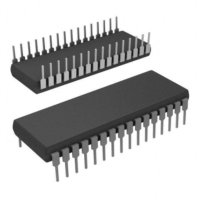
| 描述 | IC FLASH 1MBIT 70NS 32DIP闪存 128K X 8 70ns |
| 产品分类 | |
| 品牌 | Microchip Technology |
| 产品手册 | |
| 产品图片 |
|
| rohs | 符合RoHS无铅 / 符合限制有害物质指令(RoHS)规范要求 |
| 产品系列 | 内存,闪存,Microchip Technology SST39SF010A-70-4C-PHESST39 MPF™ |
| 数据手册 | 点击此处下载产品Datasheethttp://www.microchip.com/mymicrochip/filehandler.aspx?ddocname=en550334http://www.microchip.com/mymicrochip/filehandler.aspx?ddocname=en556157http://www.microchip.com/mymicrochip/filehandler.aspx?ddocname=en551028 |
| 产品型号 | SST39SF010A-70-4C-PHE |
| PCN设计/规格 | |
| 产品目录页面 | |
| 产品种类 | 闪存 |
| 供应商器件封装 | 32-PDIP |
| 其它名称 | SST39SF010A704CPHE |
| 包装 | 管件 |
| 商标 | Microchip Technology |
| 存储器类型 | FLASH |
| 存储容量 | 1M (128K x 8) |
| 存储类型 | NOR |
| 安装风格 | Through Hole |
| 定时类型 | Asynchronous |
| 封装 | Tube |
| 封装/外壳 | 32-DIP(0.600",15.24mm) |
| 封装/箱体 | PDIP-32 |
| 工作温度 | 0°C ~ 70°C |
| 工作温度范围 | 0 C to + 70 C |
| 工厂包装数量 | 11 |
| 接口 | 并联 |
| 接口类型 | Parallel |
| 数据总线宽度 | 8 bit |
| 最大工作电流 | 25 mA |
| 标准包装 | 11 |
| 格式-存储器 | 闪存 |
| 电压-电源 | 4.5 V ~ 5.5 V |
| 电源电压-最大 | 5.5 V |
| 电源电压-最小 | 4.5 V |
| 系列 | SST39SF |
| 组织 | 128 k x 8 |
| 结构 | Sector |
| 访问时间 | 70 ns |
| 速度 | 70ns |


- 商务部:美国ITC正式对集成电路等产品启动337调查
- 曝三星4nm工艺存在良率问题 高通将骁龙8 Gen1或转产台积电
- 太阳诱电将投资9.5亿元在常州建新厂生产MLCC 预计2023年完工
- 英特尔发布欧洲新工厂建设计划 深化IDM 2.0 战略
- 台积电先进制程称霸业界 有大客户加持明年业绩稳了
- 达到5530亿美元!SIA预计今年全球半导体销售额将创下新高
- 英特尔拟将自动驾驶子公司Mobileye上市 估值或超500亿美元
- 三星加码芯片和SET,合并消费电子和移动部门,撤换高东真等 CEO
- 三星电子宣布重大人事变动 还合并消费电子和移动部门
- 海关总署:前11个月进口集成电路产品价值2.52万亿元 增长14.8%
_renders/MR4A16BCYS35.jpg)


_renders/IS66WVE4M16EBLL-70BLI.jpg)
PDF Datasheet 数据手册内容提取
1 Mbit / 2 Mbit / 4 Mbit (x8) Multi-Purpose Flash SST39SF010A / SST39SF020A / SST39SF040 Data Sheet The SST39SF010A / SST39SF020A / SST39SF040 are CMOS Multi-Purpose Flash (MPF) devices manufactured with SST proprietary, high performance CMOS SuperFlash technology. The split-gate cell design and thick oxide tunnel- ing injector attain better reliability and manufacturability compared with alternate approaches. The SST39SF010A / SST39SF020A / SST39SF040 write (Program or Erase) with a 4.5-5.5V power supply, and conforms to JEDEC standard pinouts for x8 memories Features • Organized as 128K x8 / 256K x8 / 512K x8 (cid:129) Fast Erase and Byte-Program –Sector-Erase Time: 18 ms (typical) (cid:129) Single 4.5-5.5V Read and Write Operations –Chip-Erase Time: 70 ms (typical) –Byte-Program Time: 14 µs (typical) (cid:129) Superior Reliability –Chip Rewrite Time: –Endurance: 100,000 Cycles (typical) 2 seconds (typical) for SST39SF010A –Greater than 100 years Data Retention 4 seconds (typical) for SST39SF020A 8 seconds (typical) for SST39SF040 (cid:129) Low Power Consumption (typical values at 14 MHz) (cid:129) End-of-Write Detection –Active Current: 10 mA (typical) –Toggle Bit –Standby Current: 30 µA (typical) –Data# Polling (cid:129) Sector-Erase Capability (cid:129) TTL I/O Compatibility –Uniform 4 KByte sectors (cid:129) JEDEC Standard (cid:129) Fast Read Access Time: –Flash EEPROM Pinouts and command sets –55 ns –70 ns (cid:129) Packages Available –32-lead PLCC (cid:129) Latched Address and Data –32-lead TSOP (8mm x 14mm) –32-pin PDIP (cid:129) Automatic Write Timing –Internal V Generation (cid:129) All devices are RoHS compliant PP www.microchip.com ©2002-2016 DS20005022C 04/16
1 Mbit / 2 Mbit / 4 Mbit Multi-Purpose Flash SST39SF010A / SST39SF020A / SST39SF040 Data Sheet Product Description The SST39SF010A/020A/040 are CMOS Multi-Purpose Flash (MPF) manufactured with SST’s propri- etary, high performance CMOS SuperFlash technology. The split-gate cell design and thick oxide tun- neling injector attain better reliability and manufacturability compared with alternate approaches. The SST39SF010A/020A/040 devices write (Program or Erase) with a 4.5-5.5V power supply. The SST39SF010A/020A/040 devices conform to JEDEC standard pinouts for x8 memories. Featuring high performance Byte-Program, the SST39SF010A/020A/040 devices provide a maximum Byte-Program time of 20 µsec. These devices use Toggle Bit or Data# Polling to indicate the comple- tion of Program operation. To protect against inadvertent write, they have on-chip hardware and Soft- ware Data Protection schemes. Designed, manufactured, and tested for a wide spectrum of applications, these devices are offered with a guaranteed typical endurance of 100,000 cycles. Data retention is rated at greater than 100 years. The SST39SF010A/020A/040 devices are suited for applications that require convenient and econom- ical updating of program, configuration, or data memory. For all system applications, they significantly improve performance and reliability, while lowering power consumption. They inherently use less energy during erase and program than alternative flash technologies. The total energy consumed is a function of the applied voltage, current, and time of application. Since for any given voltage range, the SuperFlash technology uses less current to program and has a shorter erase time, the total energy consumed during any Erase or Program operation is less than alternative flash technologies. These devices also improve flexibility while lowering the cost for program, data, and configuration storage applications. The SuperFlash technology provides fixed Erase and Program times, independent of the number of Erase/Program cycles that have occurred. Therefore the system software or hardware does not have to be modified or de-rated as is necessary with alternative flash technologies, whose Erase and Pro- gram times increase with accumulated Erase/Program cycles. To meet high density, surface mount requirements, the SST39SF010A/020A/040 are offered in 32-lead PLCC and 32-lead TSOP packages. A 600 mil, 32-pin PDIP is also available. See Figures 2, 3, and 4 for pin assignments. ©2002-2016 DS20005022C 04/16 2
1 Mbit / 2 Mbit / 4 Mbit Multi-Purpose Flash SST39SF010A / SST39SF020A / SST39SF040 Data Sheet Block Diagram SuperFlash X-Decoder Memory Memory Address Address Buffers & Latches Y-Decoder CE# OE# Control Logic I/O Buffers and Data Latches WE# DQ7 - DQ0 1147 B1.2 Figure 1: Functional Block Diagram ©2002-2016 DS20005022C 04/16 3
1 Mbit / 2 Mbit / 4 Mbit Multi-Purpose Flash SST39SF010A / SST39SF020A / SST39SF040 Data Sheet Pin Assignment ST39SF040 A12 A15 A16 A18 VDD WE# A17 S A T39SF020 A12 A15 A16 NC VDD WE# A17 S S A T39SF010 A12 A15 A16 NC VDD WE# NC S S SST39SF040 SST39SF020A SST39SF010A SST39SF010A SST39SF020A SST39SF040 4 3 2 1 32 31 30 A7 A7 A7 5 29 A14 A14 A14 A6 A6 A6 6 28 A13 A13 A13 A5 A5 A5 7 27 A8 A8 A8 A4 A4 A4 8 26 A9 A9 A9 32-lead PLCC A3 A3 A3 9 25 A11 A11 A11 Top View A2 A2 A2 10 24 OE# OE# OE# A1 A1 A1 11 23 A10 A10 A10 A0 A0 A0 12 22 CE# CE# CE# DQ0 DQ0 DQ0 13 21 DQ7 DQ7 DQ7 14 15 16 17 18 19 20 A T39SF010 DQ1 DQ2 VSS DQ3 DQ4 DQ5 DQ6 1147 32-plcc P2.4 S S A SF020 DQ1 DQ2 VSS DQ3 DQ4 DQ5 DQ6 T39 S S F040 Q1 Q2 SS Q3 Q4 Q5 Q6 S D D V D D D D T39 S S Figure 2: Pin Assignments for 32-lead PLCC ©2002-2016 DS20005022C 04/16 4
1 Mbit / 2 Mbit / 4 Mbit Multi-Purpose Flash SST39SF010A / SST39SF020A / SST39SF040 Data Sheet SST39SF040 SST39SF020A SST39SF010A SST39SF010A SST39SF020A SST39SF040 A11 A11 A11 1 32 OE# OE# OE# A9 A9 A9 2 31 A10 A10 A10 A8 A8 A8 3 30 CE# CE# CE# A13 A13 A13 4 29 DQ7 DQ7 DQ7 A14 A14 A14 5 28 DQ6 DQ6 DQ6 Standard Pinout A17 A17 NC 6 27 DQ5 DQ5 DQ5 WE# WE# WE# 7 26 DQ4 DQ4 DQ4 Top View VDD VDD VDD 8 25 DQ3 DQ3 DQ3 A18 NC NC 9 Die Up 24 VSS VSS VSS A16 A16 A16 10 23 DQ2 DQ2 DQ2 A15 A15 A15 11 22 DQ1 DQ1 DQ1 A12 A12 A12 12 21 DQ0 DQ0 DQ0 A7 A7 A7 13 20 A0 A0 A0 A6 A6 A6 14 19 A1 A1 A1 A5 A5 A5 15 18 A2 A2 A2 A4 A4 A4 16 17 A3 A3 A3 1147 32-tsop P1.1 Figure 3: Pin Assignments for 32-lead TSOP (8mm x 14mm) SST39SF040 SST39SF020A SST39SF010A SST39SF010A SST39SF020A SST39SF040 A18 NC NC 1 32 VDD VDD VDD A16 A16 A16 2 31 WE# WE# WE# A15 A15 A15 3 30 NC A17 A17 A12 A12 A12 4 29 A14 A14 A14 A7 A7 A7 5 28 A13 A13 A13 32-pin A6 A6 A6 6 27 A8 A8 A8 A5 A5 A5 7 PDIP 26 A9 A9 A9 A4 A4 A4 8 Top View 25 A11 A11 A11 A3 A3 A3 9 24 OE# OE# OE# A2 A2 A2 10 23 A10 A10 A10 A1 A1 A1 11 22 CE# CE# CE# A0 A0 A0 12 21 DQ7 DQ7 DQ7 DQ0 DQ0 DQ0 13 20 DQ6 DQ6 DQ6 DQ1 DQ1 DQ1 14 19 DQ5 DQ5 DQ5 DQ2 DQ2 DQ2 15 18 DQ4 DQ4 DQ4 VSS VSS VSS 16 17 DQ3 DQ3 DQ3 1147 32-pdip P3.2 Figure 4: Pin Assignments for 32-pin PDIP ©2002-2016 DS20005022C 04/16 5
1 Mbit / 2 Mbit / 4 Mbit Multi-Purpose Flash SST39SF010A / SST39SF020A / SST39SF040 Data Sheet Table 1: Pin Description Symbol Pin Name Functions A 1-A Address Inputs To provide memory addresses. MS 0 During Sector-Erase A -A address lines will select the sector. MS 12 DQ -DQ Data Input/output To output data during Read cycles and receive input data during Write cycles. 7 0 Data is internally latched during a Write cycle. The outputs are in tri-state when OE# or CE# is high. CE# Chip Enable To activate the device when CE# is low. OE# Output Enable To gate the data output buffers. WE# Write Enable To control the Write operations. V Power Supply To provide 5.0V supply (4.5-5.5V) DD V Ground SS NC No Connection Unconnected pins. T1.2 25022 1. AMS = Most significant address AMS = A16 for SST39SF010A, A17 for SST39SF020A, and A18 for SST39SF040 ©2002-2016 DS20005022C 04/16 6
1 Mbit / 2 Mbit / 4 Mbit Multi-Purpose Flash SST39SF010A / SST39SF020A / SST39SF040 Data Sheet Device Operation Commands are used to initiate the memory operation functions of the device. Commands are written to the device using standard microprocessor write sequences. A command is written by asserting WE# low while keeping CE# low. The address bus is latched on the falling edge of WE# or CE#, whichever occurs last. The data bus is latched on the rising edge of WE# or CE#, whichever occurs first. Read The Read operation of the SST39SF010A/020A/040 is controlled by CE# and OE#, both have to be low for the system to obtain data from the outputs. CE# is used for device selection. When CE# is high, the chip is deselected and only standby power is consumed. OE# is the output control and is used to gate data from the output pins. The data bus is in high impedance state when either CE# or OE# is high. Refer to the Read cycle timing diagram (Figure 5) for further details. Byte-Program Operation The SST39SF010A/020A/040 are programmed on a byte-by-byte basis. Before programming, the sec- tor where the byte exists must be fully erased. The Program operation is accomplished in three steps. The first step is the three-byte load sequence for Software Data Protection. The second step is to load byte address and byte data. During the Byte-Program operation, the addresses are latched on the fall- ing edge of either CE# or WE#, whichever occurs last. The data is latched on the rising edge of either CE# or WE#, whichever occurs first. The third step is the internal Program operation which is initiated after the rising edge of the fourth WE# or CE#, whichever occurs first. The Program operation, once initiated, will be completed, within 20 µs. See Figures 6 and 7 for WE# and CE# controlled Program operation timing diagrams and Figure 16 for flowcharts. During the Program operation, the only valid reads are Data# Polling and Toggle Bit. During the internal Program operation, the host is free to per- form additional tasks. Any commands written during the internal Program operation will be ignored. Sector-Erase Operation The Sector-Erase operation allows the system to erase the device on a sector-by-sector basis. The sector architecture is based on uniform sector size of 4 KByte. The Sector-Erase operation is initiated by executing a six-byte command load sequence for Software Data Protection with Sector-Erase com- mand (30H) and sector address (SA) in the last bus cycle. The sector address is latched on the falling edge of the sixth WE# pulse, while the command (30H) is latched on the rising edge of the sixth WE# pulse. The internal Erase operation begins after the sixth WE# pulse. The End-of-Erase can be deter- mined using either Data# Polling or Toggle Bit methods. See Figure 10 for timing waveforms. Any com- mands written during the Sector-Erase operation will be ignored. Chip-Erase Operation The SST39SF010A/020A/040 provide Chip-Erase operation, which allows the user to erase the entire memory array to the “1s” state. This is useful when the entire device must be quickly erased. The Chip-Erase operation is initiated by executing a six- byte Software Data Protection command sequence with Chip-Erase command (10H) with address 5555H in the last byte sequence. The internal Erase operation begins with the rising edge of the sixth WE# or CE#, whichever occurs first. During the internal Erase operation, the only valid read is Toggle Bit or Data# Polling. See Table 4 for the com- mand sequence, Figure 11 for timing diagram, and Figure 19 for the flowchart. Any commands written during the Chip-Erase operation will be ignored. ©2002-2016 DS20005022C 04/16 7
1 Mbit / 2 Mbit / 4 Mbit Multi-Purpose Flash SST39SF010A / SST39SF020A / SST39SF040 Data Sheet Write Operation Status Detection The SST39SF010A/020A/040 provide two software means to detect the completion of a Write (Pro- gram or Erase) cycle, in order to optimize the system Write cycle time. The software detection includes two status bits: Data# Polling (DQ ) and Toggle Bit (DQ ). The End-of-Write detection mode is enabled 7 6 after the rising edge of WE# which initiates the internal Program or Erase operation. The actual completion of the nonvolatile write is asynchronous with the system; therefore, either a Data# Polling or Toggle Bit read may be simultaneous with the completion of the Write cycle. If this occurs, the system may possibly get an erroneous result, i.e., valid data may appear to conflict with either DQ or DQ . In order to prevent spurious rejection, if an erroneous result occurs, the software 7 6 routine should include a loop to read the accessed location an additional two (2) times. If both reads are valid, then the device has completed the Write cycle, otherwise the rejection is valid. Data# Polling (DQ ) 7 When the SST39SF010A/020A/040 are in the internal Program operation, any attempt to read DQ will 7 produce the complement of the true data. Once the Program operation is completed, DQ will produce 7 true data. Note that even though DQ mayhave valid data immediately following the completion of an 7 internal Write operation, the remaining data outputs may still be invalid: valid data on the entire data bus will appear in subsequent successive Read cycles after an interval of 1 µs. During internal Erase operation, any attempt to read DQ will produce a ‘0’. Once the internal Erase operation is completed, 7 DQ will produce a ‘1’. The Data# Polling is valid after the rising edge of fourth WE# (or CE#) pulse for 7 Program operation. For Sector- or Chip-Erase, the Data# Polling is valid after the rising edge of sixth WE# (or CE#) pulse. See Figure 8 for Data# Polling timing diagram and Figure 17 for a flowchart. Toggle Bit (DQ ) 6 During the internal Program or Erase operation, any consecutive attempts to read DQ will produce 6 alternating 0s and 1s, i.e., toggling between 0 and 1. When the internal Program or Erase operation is completed, the toggling will stop. The device is then ready for the next operation. The Toggle Bit is valid after the rising edge of fourth WE# (or CE#) pulse for Program operation. For Sector- or Chip-Erase, the Toggle Bit is valid after the rising edge of sixth WE# (or CE#) pulse. See Figure 9 for Toggle Bit tim- ing diagram and Figure 17 for a flowchart. Data Protection The SST39SF010A/020A/040 provide both hardware and software features to protect nonvolatile data from inadvertent writes. Hardware Data Protection Noise/Glitch Protection: A WE# or CE# pulse of less than 5 ns will not initiate a Write cycle. V Power Up/Down Detection: The Write operation is inhibited when V is less than 2.5V. DD DD Write Inhibit Mode: Forcing OE# low, CE# high, or WE# high will inhibit the Write operation. This pre- vents inadvertent writes during power-up or power-down. ©2002-2016 DS20005022C 04/16 8
1 Mbit / 2 Mbit / 4 Mbit Multi-Purpose Flash SST39SF010A / SST39SF020A / SST39SF040 Data Sheet Software Data Protection (SDP) The SST39SF010A/020A/040 provide the JEDEC approved Software Data Protection scheme for all data alteration operations, i.e., Program and Erase. Any Program operation requires the inclusion of a series of three-byte sequence. The three-byte load sequence is used to initiate the Program operation, providing optimal protection from inadvertent Write operations, e.g., during the system power-up or power-down. Any Erase operation requires the inclusion of six-byte load sequence. The SST39SF010A/020A/040 devices are shipped with the Software Data Protection permanently enabled. See Table 4 for the specific software command codes. During SDP command sequence, invalid commands will abort the device to read mode, within T RC. Product Identification The Product Identification mode identifies the device as the SST39SF040, SST39SF010A, or SST39SF020A and manufacturer as SST. This mode may be accessed by software operations. Users may wish to use the software Product Identification operation to identify the part (i.e., using the device ID) when using multiple manufacturers in the same socket. For details, Table 4 for software operation, Figure 12 for the software ID entry and read timing diagram and Figure 18 for the ID entry command sequence flowchart. Table 2: Product Identification Address Data Manufacturer’s ID 0000H BFH Device ID SST39SF010A 0001H B5H SST39SF020A 0001H B6H SST39SF040 0001H B7H T2.2 25022 Product Identification Mode Exit/Reset In order to return to the standard Read mode, the Software Product Identification mode must be exited. Exit is accomplished by issuing the Exit ID command sequence, which returns the device to the Read operation. Please note that the software reset command is ignored during an internal Program or Erase operation. See Table 4 for software command codes, Figure 13 for timing waveform and Figure 18 for a flowchart. ©2002-2016 DS20005022C 04/16 9
1 Mbit / 2 Mbit / 4 Mbit Multi-Purpose Flash SST39SF010A / SST39SF020A / SST39SF040 Data Sheet Operations Table 3: Operation Modes Selection Mode CE# OE# WE# DQ Address Read V V V D A IL IL IH OUT IN Program V V V D A IL IH IL IN IN Erase V V V X1 Sector address, XXH for Chip-Erase IL IH IL Standby V X X High Z X IH Write Inhibit X V X High Z/ D X IL OUT X X V High Z/ D X IH OUT Product Identification Software Mode V V V See Table 4 IL IL IH T3.3 25022 1. X can be VIL or VIH, but no other value. Table 4: Software Command Sequence Command 1st Bus 2nd Bus 3rd Bus 4th Bus 5th Bus 6th Bus Sequence Write Cycle Write Cycle Write Cycle Write Cycle Write Cycle Write Cycle Addr1 Data Addr1 Data Addr1 Data Addr1 Data Addr1 Data Addr1 Data Byte-Program 5555H AAH 2AAAH 55H 5555H A0H BA2 Data Sector-Erase 5555H AAH 2AAAH 55H 5555H 80H 5555H AAH 2AAAH 55H SA 3 30H X Chip-Erase 5555H AAH 2AAAH 55H 5555H 80H 5555H AAH 2AAAH 55H 5555H 10H Software ID Entry4,5 5555H AAH 2AAAH 55H 5555H 90H Software ID Exit6 XXH F0H Software ID Exit6 5555H AAH 2AAAH 55H 5555H F0H T4.2 25022 1. Address format A14-A0 (Hex), Addresses AMS-A15 can be VIL or VIH, but no other value, for the Command sequence. AMS = Most significant address AMS = A16 for SST39SF010A, A17 for SST39SF020A, and A18 for SST39SF040 2. BA = Program Byte address 3. SAX for Sector-Erase; uses AMS-A12 address lines 4. The device does not remain in Software Product ID mode if powered down. 5. With AMS-A1 = 0; SST Manufacturer’s ID = BFH, is read with A0 = 0, SST39SF010A Device ID = B5H, is read with A0 = 1 SST39SF020A Device ID = B6H, is read with A0 = 1 SST39SF040 Device ID = B7H, is read with A0 = 1 6. Both Software ID Exit operations are equivalent ©2002-2016 DS20005022C 04/16 10
1 Mbit / 2 Mbit / 4 Mbit Multi-Purpose Flash SST39SF010A / SST39SF020A / SST39SF040 Data Sheet Absolute Maximum Stress Ratings (Applied conditions greater than those listed under “Absolute Maximum Stress Ratings” may cause permanent damage to the device. This is a stress rating only and functional operation of the device at these conditions or conditions greater than those defined in the operational sections of this data sheet is not implied. Exposure to absolute maximum stress rating con- ditions may affect device reliability.) Temperature Under Bias . . . . . . . . . . . . . . . . . . . . . . . . . . . . . . . . . . . . . . . . . . . . . . -55°C to +125°C Storage Temperature . . . . . . . . . . . . . . . . . . . . . . . . . . . . . . . . . . . . . . . . . . . . . . . . -65°C to +150°C D. C. Voltage on Any Pin to Ground Potential . . . . . . . . . . . . . . . . . . . . . . . . . . . . .-0.5V to V +0.5V DD Transient Voltage (<20 ns) on Any Pin to Ground Potential . . . . . . . . . . . . . . . . . .-2.0V to V +2.0V DD Voltage on A Pin to Ground Potential . . . . . . . . . . . . . . . . . . . . . . . . . . . . . . . . . . . . . -0.5V to 13.2V 9 Package Power Dissipation Capability (Ta = 25°C) . . . . . . . . . . . . . . . . . . . . . . . . . . . . . . . . . . 1.0W Through Hold Lead Soldering Temperature (10 Seconds) . . . . . . . . . . . . . . . . . . . . . . . . . . . . .300°C Surface Mount Lead Soldering Temperature (3 Seconds) . . . . . . . . . . . . . . . . . . . . . . . . . . . . .240°C Output Short Circuit Current1 . . . . . . . . . . . . . . . . . . . . . . . . . . . . . . . . . . . . . . . . . . . . . . . . . 100 mA 1. Outputs shorted for no more than one second. No more than one output shorted at a time. Table 5: Operating Range Range Ambient Temp V DD Commercial 0°C to +70°C 4.5-5.5V Industrial -40°C to +85°C 4.5-5.5V T5.1 25022 Table 6: AC Conditions of Test1 Input Rise/Fall Time Output Load 5ns C = 30 pF for 55 ns L C = 100 pF for 70 ns L T6.1 25022 1. See Figures 14 and 15 ©2002-2016 DS20005022C 04/16 11
1 Mbit / 2 Mbit / 4 Mbit Multi-Purpose Flash SST39SF010A / SST39SF020A / SST39SF040 Data Sheet Table 7: DC Operating Characteristics V = 4.5-5.5V1 DD Limits Symbol Parameter Min Max Units Test Conditions I Power Supply Current Address input=V /V , at f=1/T Min DD ILT IHT RC V =V Max DD DD Read2 25 mA CE#=V , OE#=WE#=V , all I/Os open IL IH Program and Erase 35 mA CE#=WE#=V , OE#=V IL IH I Standby V Current 3 mA CE#=V , V =V Max SB1 DD IH DD DD (TTL input) I Standby V Current 100 µA CE#=V , V =V Max SB2 DD IHC DD DD (CMOS input) I Input Leakage Current 1 µA V =GND to V , V =V Max LI IN DD DD DD I Output Leakage Current 10 µA V =GND to V , V =V Max LO OUT DD DD DD V Input Low Voltage 0.8 V V =V Min IL DD DD V Input High Voltage 2.0 V V =V Max IH DD DD V Input High Voltage (CMOS) V -0.3 V V =V Max IHC DD DD DD V Output Low Voltage 0.4 V I =2.1 mA, V =V Min OL OL DD DD V Output High Voltage 2.4 V I =-400 µA, V =V Min OH OH DD DD T7.10 25022 1. Typical conditions for the Active Current shown on the front data sheet page are average values at 25°C (room temperature), and VDD = 5V for SF devices. Not 100% tested. 2. Values are for 70 ns conditions. See the Multi-Purpose Flash Power Rating application note for further information. Table 8: Recommended System Power-up Timings Symbol Parameter Minimum Units T 1 Power-up to Read Operation 100 µs PU-READ T 1 Power-up to Program/Erase Operation 100 µs PU-WRITE T8.1 25022 1. This parameter is measured only for initial qualification and after a design or process change that could affect this parameter. Table 9: Capacitance (Ta = 25°C, f=1 Mhz, other pins open) Parameter Description Test Condition Maximum C 1 I/O Pin Capacitance V = 0V 12 pF I/O I/O C 1 Input Capacitance V = 0V 6 pF IN IN T9.0 25022 1. This parameter is measured only for initial qualification and after a design or process change that could affect this parameter. Table 10:Reliability Characteristics Symbol Parameter Minimum Specification Units Test Method N 1,2 Endurance 10,000 Cycles JEDEC Standard A117 END T 1 Data Retention 100 Years JEDEC Standard A103 DR I 1 Latch Up 100 + I mA JEDEC Standard 78 LTH DD T10.225022 1. This parameter is measured only for initial qualification and after a design or process change that could affect this parameter. 2. NEND endurance rating is qualified as a 10,000 cycle minimum for the whole device. A sector- or block-level rating would result in a higher minimum specification. ©2002-2016 DS20005022C 04/16 12
1 Mbit / 2 Mbit / 4 Mbit Multi-Purpose Flash SST39SF010A / SST39SF020A / SST39SF040 Data Sheet AC Characteristics Table 11:Read Cycle Timing Parameters V = 4.5-5.5V DD SST39SF010A/020A/040-55 SST39SF010A/020A/040-70 Symbol Parameter Min Max Min Max Units T Read Cycle Time 55 70 ns RC T Chip Enable Access Time 55 70 ns CE T Address Access Time 55 70 ns AA T Output Enable Access Time 35 35 ns OE T 1 CE# Low to Active Output 0 0 ns CLZ T 1 OE# Low to Active Output 0 0 ns OLZ T 1 CE# High to High-Z Output 20 25 ns CHZ T 1 OE# High to High-Z Output 20 25 ns OHZ T 1 Output Hold from Address Change 0 0 ns OH T11.425022 1. This parameter is measured only for initial qualification and after a design or process change that could affect this parameter. Table 12:Program/Erase Cycle Timing Parameters Symbol Parameter Min Max Units T Byte-Program Time 20 µs BP T Address Setup Time 0 ns AS T Address Hold Time 30 ns AH T WE# and CE# Setup Time 0 ns CS T WE# and CE# Hold Time 0 ns CH T OE# High Setup Time 0 ns OES T OE# High Hold Time 10 ns OEH T CE# Pulse Width 40 ns CP T WE# Pulse Width 40 ns WP T 1 WE# Pulse Width High 30 ns WPH T 1 CE# Pulse Width High 30 ns CPH T Data Setup Time 40 ns DS T 1 Data Hold Time 0 ns DH T 1 Software ID Access and Exit Time 150 ns IDA T Sector-Erase 25 ms SE T Chip-Erase 100 ms SCE T12.1 25022 1. This parameter is measured only for initial qualification and after a design or process change that could affect this parameter. ©2002-2016 DS20005022C 04/16 13
1 Mbit / 2 Mbit / 4 Mbit Multi-Purpose Flash SST39SF010A / SST39SF020A / SST39SF040 Data Sheet TRC TAA ADDRESS AMS-0 TCE CE# TOE OE# VIH TOLZ TOHZ WE# TCLZ TOH TCHZ HIGH-Z HIGH-Z DQ7-0 DATA VALID DATA VALID 1147 F03.1 Note: AMS = Most significant address AMS = A16 for SST39SF010A, A17 for SST39SF020A, and A18 for SST39SF040 Figure 5: Read Cycle Timing Diagram INTERNAL PROGRAM OPERATION STARTS TBP ADDRESS AMS-0 5555 2AAA 5555 ADDR TAH TWP TDH WE# TAS TWPH TDS OE# TCH CE# TCS DQ7-0 AA 55 A0 DATA SW0 SW1 SW2 BYTE (ADDR/DATA) 1147 F04.1 Note: AMS = Most significant address AMS = A16 for SST39SF010A, A17 for SST39SF020A, and A18 for SST39SF040 Figure 6: WE# Controlled Program Cycle Timing Diagram ©2002-2016 DS20005022C 04/16 14
1 Mbit / 2 Mbit / 4 Mbit Multi-Purpose Flash SST39SF010A / SST39SF020A / SST39SF040 Data Sheet INTERNAL PROGRAM OPERATION STARTS TBP ADDRESS AMS-0 5555 2AAA 5555 ADDR TAH TCP TDH CE# TAS TCPH TDS OE# TCH WE# TCS DQ7-0 AA 55 A0 DATA SW0 SW1 SW2 BYTE (ADDR/DATA) 1147 F05.1 Note: AMS = Most significant address AMS = A16 for SST39SF010A, A17 for SST39SF020A, and A18 for SST39SF040 Figure 7: CE# Controlled Program Cycle Timing Diagram ADDRESS AMS-0 TCE CE# TOEH TOES OE# TOE WE# DQ7 D D# D# D 1147 F06.1 Note: AMS = Most significant address AMS = A16 for SST39SF010A, A17 for SST39SF020A, and A18 for SST39SF040 Figure 8: Data# Polling Timing Diagram ©2002-2016 DS20005022C 04/16 15
1 Mbit / 2 Mbit / 4 Mbit Multi-Purpose Flash SST39SF010A / SST39SF020A / SST39SF040 Data Sheet ADDRESS AMS-0 TCE CE# TOEH TOES TOE OE# WE# DQ6 Note TWO READ CYCLES WITH SAME OUTPUTS 1147 F07.1 Note: Toggled bit output is always high first. AMS = Most significant address AMS = A16 for SST39SF010A, A17 for SST39SF020A, and A18 for SST39SF040 Figure 9: Toggle Bit Timing Diagram SIX-BYTE CODE FOR SECTOR-ERASE TSE ADDRESS AMS-0 5555 2AAA 5555 5555 2AAA SAX CE# OE# TWP WE# DQ7-0 AA 55 80 AA 55 30 SW0 SW1 SW2 SW3 SW4 SW5 1147 F08.1 Note: This device also supports CE# controlled Sector-Erase operation. The WE# and CE# signals are interchangeable as long as minimum timings are met. (See Table 10) SAXX = Sector Address Toggled bit output is always high first. AMS = Most significant address AMS = A16 for SST39SF010A, A17 for SST39SF020A, and A18 for SST39SF040 Figure 10:WE# Controlled Sector-Erase Timing Diagram ©2002-2016 DS20005022C 04/16 16
1 Mbit / 2 Mbit / 4 Mbit Multi-Purpose Flash SST39SF010A / SST39SF020A / SST39SF040 Data Sheet SIX-BYTE CODE FOR CHIP-ERASE TSCE ADDRESS AMS-0 5555 2AAA 5555 5555 2AAA 5555 CE# OE# TWP WE# DQ7-0 AA 55 80 AA 55 10 SW0 SW1 SW2 SW3 SW4 SW5 1147 F17.1 Note: This device also supports CE# controlled Sector-Erase operation. The WE# and CE# signals are interchangeable as long as minimum timings are met. (See Table 10) SAXX = Sector Address Toggled bit output is always high first. AMS = Most significant address Figure 11:WE# Controlled Chip-Erase Timing Diagram Three-byte Sequence for Software ID Entry ADDRESS A14-0 5555 2AAA 5555 0000 0001 CE# OE# TWP TIDA WE# TWPH TAA DQ7-0 AA 55 90 BF Device ID SW0 SW1 SW2 1147 F09.2 Note: Device ID = B5H for SST39SF010A, B6H for SST39SF020A, and B7H for SST39SF040 Figure 12:Software ID Entry and Read ©2002-2016 DS20005022C 04/16 17
1 Mbit / 2 Mbit / 4 Mbit Multi-Purpose Flash SST39SF010A / SST39SF020A / SST39SF040 Data Sheet THREE-BYTE SEQUENCE FOR SOFTWARE ID EXIT AND RESET ADDRESS A14-0 5555 2AAA 5555 DQ7-0 AA 55 F0 TIDA CE# OE# TWP WE# TWHP SW0 SW1 SW2 1147 F10.0 Figure 13:Software ID Exit and Reset VIHT INPUT VIT REFERENCE POINTS VOT OUTPUT VILT 1147 F11.1 AC test inputs are driven at V (3.0V) for a logic “1” and V (0V) for a logic “0”. Measure- IHT ILT ment reference points for inputs and outputs are V (1.5V) and V (1.5V). Input rise IT OT Note: VIT - VINPUT Test VOT - VOUTPUT Test VIHT - VINPUT HIGH Test VILT - VINPUT LOW Test Figure 14:AC Input/Output Reference Waveforms VDD TO TESTER RL HIGH TO DUT CL RL LOW 1147 F12.0 Figure 15:A Test Load Example ©2002-2016 DS20005022C 04/16 18
1 Mbit / 2 Mbit / 4 Mbit Multi-Purpose Flash SST39SF010A / SST39SF020A / SST39SF040 Data Sheet Start Load data: AAH Address: 5555H Load data: 55H Address: 2AAAH Load data: A0H Address: 5555H Load Byte Address/Byte Data Wait for end of Program (TBP, Data# Polling bit, or Toggle bit operation) Program Completed 1147 F13.1 Figure 16:Byte-Program Algorithm ©2002-2016 DS20005022C 04/16 19
1 Mbit / 2 Mbit / 4 Mbit Multi-Purpose Flash SST39SF010A / SST39SF020A / SST39SF040 Data Sheet Internal Timer Toggle Bit Data# Polling Byte Byte Byte Program/Erase Program/Erase Program/Erase Initiated Initiated Initiated Read byte Read DQ7 Wait TBP, TSCE, or TSE Read same No Is DQ7 = byte true data? Program/Erase Completed Yes No Does DQ6 Program/Erase match? Completed Yes Program/Erase Completed 1147 F14.0 Figure 17:Wait Options ©2002-2016 DS20005022C 04/16 20
1 Mbit / 2 Mbit / 4 Mbit Multi-Purpose Flash SST39SF010A / SST39SF020A / SST39SF040 Data Sheet Software Product ID Entry Software Product ID Exit & Command Sequence Reset Command Sequence Load data: AAH Load data: AAH Load data: F0H Address: 5555H Address: 5555H Address: XXH Load data: 55H Load data: 55H Wait TIDA Address: 2AAAH Address: 2AAAH Load data: 90H Load data: F0H Return to normal Address: 5555H Address: 5555H operation Wait TIDA Wait TIDA Return to normal Read Software ID operation 1147 F15.1 Figure 18:Software Product Command Flowcharts ©2002-2016 DS20005022C 04/16 21
1 Mbit / 2 Mbit / 4 Mbit Multi-Purpose Flash SST39SF010A / SST39SF020A / SST39SF040 Data Sheet Chip-Erase Sector-Erase Command Sequence Command Sequence Load data: AAH Load data: AAH Address: 5555H Address: 5555H Load data: 55H Load data: 55H Address: 2AAAH Address: 2AAAH Load data: 80H Load data: 80H Address: 5555H Address: 5555H Load data: AAH Load data: AAH Address: 5555H Address: 5555H Load data: 55H Load data: 55H Address: 2AAAH Address: 2AAAH Load data: 10H Load data: 30H Address: 5555H Address: SAX Wait TSCE Wait TSE Chip erased Sector erased to FFH to FFH 1147 F16.1 Figure 19:Erase Command Sequence ©2002-2016 DS20005022C 04/16 22
1 Mbit / 2 Mbit / 4 Mbit Multi-Purpose Flash SST39SF010A / SST39SF020A / SST39SF040 Data Sheet Product Ordering Information SST 39 SF 010A - 70 - 4C - NHE XX XX XXXX - XX - XX - XXX Environmental Attribute E1 = non-Pb Package Modifier H = 32 pins or leads Package Type N = PLCC P = PDIP W = TSOP (type 1, die up, 8mm x 14mm) Temperature Range C = Commercial = 0°C to +70°C I = Industrial = -40°C to +85°C Minimum Endurance 4 = 10,000 cycles Read Access Speed 55 = 55 ns 70 = 70 ns Version A = Special Feature Version Device Density 040 = 4 Mbit 020 = 2 Mbit 010 = 1 Mbit Voltage S = 4.5-5.5V Product Series 39 = Multi-Purpose Flash 1. Environmental suffix “E” denotes non-Pb solder. SST non-Pb solder devices are “RoHS Compli- ant”. ©2002-2016 DS20005022C 04/16 23
1 Mbit / 2 Mbit / 4 Mbit Multi-Purpose Flash SST39SF010A / SST39SF020A / SST39SF040 Data Sheet Valid combinations for SST39SF010A SST39SF010A-55-4C-NHE SST39SF010A-55-4C-WHE SST39SF010A-70-4C-NHE SST39SF010A-70-4C-WHE SST39SF010A-70-4C-PHE SST39SF010A-55-4I-NHE SST39SF010A-55-4I-WHE SST39SF010A-70-4I-NHE SST39SF010A-70-4I-WHE Valid combinations for SST39SF020A SST39SF020A-55-4C-NHE SST39SF020A-55-4C-WHE SST39SF020A-70-4C-NHE SST39SF020A-70-4C-WHE SST39SF020A-70-4C-PHE SST39SF020A-55-4I-NHE SST39SF020A-55-4I-WHE SST39SF020A-70-4I-NHE SST39SF020A-70-4I-WHE Valid combinations for SST39SF040 SST39SF040-55-4C-NHE SST39SF040-55-4C-WHE SST39SF040-70-4C-NHE SST39SF040-70-4C-WHE SST39SF040-70-4C-PHE SST39SF040-55-4I-NHE SST39SF040-55-4I-WHE SST39SF040-70-4I-NHE SST39SF040-70-4I-WHE Note:Valid combinations are those products in mass production or will be in mass production. Consult your SST sales representative to confirm availability of valid combinations and to determine availability of new combi- nations. ©2002-2016 DS20005022C 04/16 24
1 Mbit / 2 Mbit / 4 Mbit Multi-Purpose Flash SST39SF010A / SST39SF020A / SST39SF040 Data Sheet Packaging Diagrams TOP VIEW SIDE VIEW BOTTOM VIEW .495 .485 .112 Optional .453 .106 Pin #1 .447 Identifier .048 .020 R. .029x 30° .040R. .042 2 1 32 MAX. .023 .030 .042 .021 .048 .013 .595 .553 .032 .400 .530 .585 .547 .026 BSC .490 .050 BSC .015 Min. .095 .050 .075 BSC .032 .140 .026 .125 Note: 1. Complies with JEDEC publication 95 MS-016 AE dimensions, although some dimensions may be more stringent. 2. All linear dimensions are in inches (max/min). 3. Dimensions do not include mold flash. Maximum allowable mold flash is .008 inches. 4. Coplanarity: 4 mils. 32-plcc-NH-3 Figure 20:32-lead Plastic Lead Chip Carrier (PLCC) SST Package Code: NH ©2002-2016 DS20005022C 04/16 25
1 Mbit / 2 Mbit / 4 Mbit Multi-Purpose Flash SST39SF010A / SST39SF020A / SST39SF040 Data Sheet 1.05 0.95 Pin # 1 Identifier 0.50 BSC 8.10 0.27 7.90 0.17 0.15 12.50 0.05 12.30 DETAIL 1.20 max. 0.70 0.50 14.20 13.80 0°- 5° 0.70 0.50 Note: 1. Complies with JEDEC publication 95 MO-142 BA dimensions, although some dimensions may be more stringent. 2. All linear dimensions are in millimeters (max/min). 1mm 32-tsop-WH-7 3. Coplanarity: 0.1 mm 4. Maximum allowable mold flash is 0.15 mm at the package ends, and 0.25 mm between leads. Figure 21:32-lead Thin Small Outline Package (TSOP) 8mm x 14mm SST Package Code: WH ©2002-2016 DS20005022C 04/16 26
1 Mbit / 2 Mbit / 4 Mbit Multi-Purpose Flash SST39SF010A / SST39SF020A / SST39SF040 Data Sheet 32 C L 1 Pin #1 Identifier .625 .600 .550 .530 .075 1.655 7° .065 1.645 4 PLCS. Base .200 Plane .170 Seating Plane .050 0° .015 .012 15° .150 .008 .080 .065 .022 .100 BSC .120 .600 BSC .070 .045 .016 Note: 1. Complies with JEDEC publication 95 MO-015 AP dimensions, although some dimensions may be more stringent. 2. All linear dimensions are in inches (max/min). 3. Dimensions do not include mold flash. Maximum allowable mold flash is .010 inches. 32-pdip-PH-3 Figure 22:32-pin Plastic Dual In-line Pins (PDIP) SST Package Code: PH ©2002-2016 DS20005022C 04/16 27
1 Mbit / 2 Mbit / 4 Mbit Multi-Purpose Flash SST39SF010A / SST39SF020A / SST39SF040 Data Sheet Table 13:Revision History Revision Description Date 02 (cid:129) 2002 Data Book May 2002 03 (cid:129) Changes to Table 7 on page12 Mar 2003 (cid:129) Added footnote for MPF power usage and Typical conditions (cid:129) Clarified the Test Conditions for Power Supply Current and Read parameters (cid:129) Clarified I Write to be Program and Erase DD 04 (cid:129) Document status changed from “Preliminary Specification” to “Data Oct 2003 Sheet” (cid:129) Changed I Program and Erase max values from 25 to 35 in Table 7 DD on page12 05 (cid:129) 2004 Data Book Nov 2003 (cid:129) Added non-Pb MPNs and removed footnote (See page24) 06 (cid:129) Corrected Revision History for Version 04: Aug 2004 I max value was incorrectly stated as 30 mA instead of 35 mA DD 07 (cid:129) Removed leaded parts from valid combinations. See PSN-D0PB0001 Mar 2009 08 (cid:129) Changed endurance from 10,000 to 100,000 in Product Description, Sep 2009 page 1 09 (cid:129) End of Life for all 45 ns valid combinations. See S71147(02). Jan 2010 (cid:129) Added replacement 55 ns valid combinations A (cid:129) All 45 ns parts reinstated. Jul 2011 (cid:129) Applied new document format (cid:129) Released document under letter revision system (cid:129) Updated spec number from S71147 to DS25022 B (cid:129) End of Life for all 45 ns valid combinations. Apr 2013 (cid:129) Updated Table 6 and Table 11 C (cid:129) Corrected typo in “Product Ordering Information” on page23. Apr 2016 ©2002-2016 DS20005022C 04/16 28
1 Mbit / 2 Mbit / 4 Mbit Multi-Purpose Flash SST39SF010A / SST39SF020A / SST39SF040 Data Sheet ISBN:978-1-5224-0456-9 © 2016 Microchip Technology Inc. SST, Silicon Storage Technology, the SST logo, SuperFlash, and MTP are registered trademarks of Microchip Technology, Inc. MPF, SQI, Serial Quad I/O, and Z-Scale are trademarks of Microchip Technology, Inc. All other trademarks and registered trade- marks mentioned herein are the property of their respective owners. Specifications are subject to change without notice. Refer to www.microchip.com for the most recent documentation. For the most current package drawings, please see the Packaging Specification located at http://www.microchip.com/packaging. Memory sizes denote raw storage capacity; actual usable capacity may be less. Microchip makes no warranty for the use of its products other than those expressly contained in the Standard Terms and Conditions of Sale. For sales office locations and information, please see www.microchip.com. www.microchip.com ©2002-2016 DS20005022C 04/16 29