ICGOO在线商城 > 射频/IF 和 RFID > RF 放大器 > SST12LP15B-QVCE
 Datasheet下载
- 型号: SST12LP15B-QVCE
- 制造商: Microchip
- 库位|库存: xxxx|xxxx
- 要求:
| 数量阶梯 | 香港交货 | 国内含税 |
| +xxxx | $xxxx | ¥xxxx |
查看当月历史价格
查看今年历史价格
SST12LP15B-QVCE产品简介:
ICGOO电子元器件商城为您提供SST12LP15B-QVCE由Microchip设计生产,在icgoo商城现货销售,并且可以通过原厂、代理商等渠道进行代购。 SST12LP15B-QVCE价格参考。MicrochipSST12LP15B-QVCE封装/规格:RF 放大器, 射频放大器 IC 802.11b/g/n 2.4GHz 16-VQFN(3x3)。您可以下载SST12LP15B-QVCE参考资料、Datasheet数据手册功能说明书,资料中有SST12LP15B-QVCE 详细功能的应用电路图电压和使用方法及教程。
Microchip Technology的SST12LP15B-QVCE是一款高性能、低噪声射频(RF)放大器,广泛应用于无线通信系统中,以提升信号质量和传输距离。该器件采用先进的GaAs HBT工艺制造,具备良好的线性度和高增益特性,适用于多种无线通信标准和频段。

其主要应用场景包括:

1. 无线基站和接入点:用于增强上行链路信号强度,提高通信稳定性和覆盖范围,适用于Wi-Fi、LTE、5G等基础设施设备。

2. 工业通信设备:如工业级无线网桥、远程监控系统和工业物联网(IIoT)设备,提升信号传输质量与抗干扰能力。

3. 测试与测量设备:在频谱分析仪、信号发生器等仪器中用于放大微弱信号,以确保测试精度和灵敏度。

4. 军事与航空航天领域:适用于对可靠性要求高的通信系统,如战术通信设备和卫星通信终端。

5. 广播与多媒体传输系统:用于DVB-T、FM广播等系统的信号增强,保障高质量音频和视频传输。

SST12LP15B-QVCE凭借其低功耗、高稳定性和紧凑封装,特别适合空间受限且对性能要求高的应用场合。
| 参数 | 数值 |
| 产品目录 | |
| 描述 | IC RF PWR AMP 802.11B/G/N 16VQFN |
| 产品分类 | |
| 品牌 | Microchip Technology |
| 数据手册 | http://www.microchip.com/mymicrochip/filehandler.aspx?ddocname=en553515http://www.microchip.com/mymicrochip/filehandler.aspx?ddocname=en559924 |
| 产品图片 |
|
| P1dB | 29dBm |
| 产品型号 | SST12LP15B-QVCE |
| PCN设计/规格 | http://www.microchip.com/mymicrochip/NotificationDetails.aspx?id=6067&print=view |
| RF类型 | 802.11b/g/n |
| rohs | 无铅 / 符合限制有害物质指令(RoHS)规范要求 |
| 产品系列 | - |
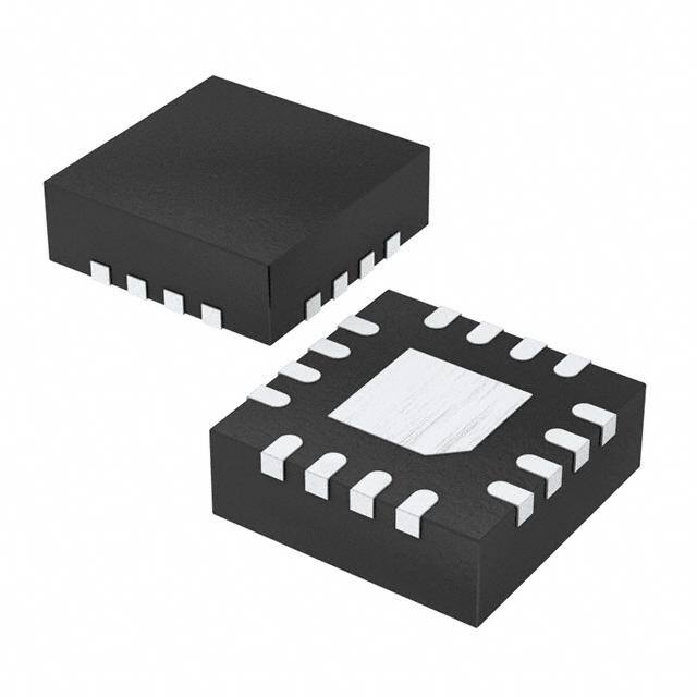
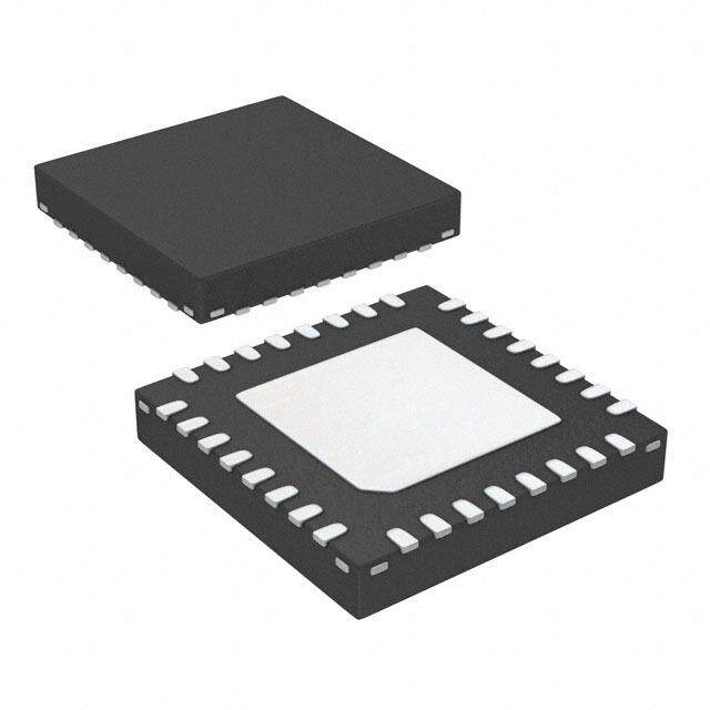
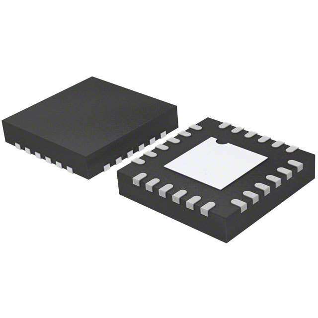
| 供应商器件封装 | 16-VQFN(3x3) |
| 其它名称 | SST12LP15B-QVCECT |
| 包装 | 剪切带 (CT) |
| 噪声系数 | - |
| 增益 | 32dB |
| 封装/外壳 | 16-VFQFN 裸露焊盘 |
| 标准包装 | 1 |
| 测试频率 | - |
| 电压-电源 | 3 V ~ 4.2 V |
| 电流-电源 | 370mA |
| 频率 | 2.4GHz |


- 商务部:美国ITC正式对集成电路等产品启动337调查
- 曝三星4nm工艺存在良率问题 高通将骁龙8 Gen1或转产台积电
- 太阳诱电将投资9.5亿元在常州建新厂生产MLCC 预计2023年完工
- 英特尔发布欧洲新工厂建设计划 深化IDM 2.0 战略
- 台积电先进制程称霸业界 有大客户加持明年业绩稳了
- 达到5530亿美元!SIA预计今年全球半导体销售额将创下新高
- 英特尔拟将自动驾驶子公司Mobileye上市 估值或超500亿美元
- 三星加码芯片和SET,合并消费电子和移动部门,撤换高东真等 CEO
- 三星电子宣布重大人事变动 还合并消费电子和移动部门
- 海关总署:前11个月进口集成电路产品价值2.52万亿元 增长14.8%


PDF Datasheet 数据手册内容提取
2.4 GHz WLAN 802.11b,g,n, 256 QAM Power Amplifier SST12LP15B Data Sheet SST12LP15B is a versatile power amplifier based on the highly-reliable InGaP/ GaAs HBT technology. Easily configured for high-linear operation meeting the EVM requirements for 256 QAM applications, and for high-efficiency applications with excellent power-added efficiency while operating over the 2.4- 2.5 GHz fre- quency band. Configured for high efficiency, SST12LP15B will typically meet the 802.11g spectrum mask at 23 dBm with 270 mA. Configured for high linearity, SST12LP15B will provide less than 2.5% EVM, up to 20 dBm, with MCS7-HT40 modulation, and less than 1.75% EVM, up to 18 dBm, with MCS9-VHT40 modula- tion. This power amplifier also features easy board-level usage along with high- speed power-up/down control through the reference voltage pins. The SST12LP15B is offered in both a 3mm x 3mm, 16-contact VQFN package and a 2mmx 2mm, 12-contact XQFN package. Features • High Gain: (cid:129) High temperature stability –More than 32 dB gain across 2.4–2.5 GHz over tempera- –Typically 1 dB gain/power variation between 0°C to ture -40°C to +85°C +85°C (cid:129) Configured for High Linearity (cid:129) Excellent On-chip power detection –20 dBm at 2.5% DEVM, MCS7-HT40, 200mA –20 dB linear dynamic range –18 dBm at 1.8% DEVM, MCS9-VHT40, 180 mA –Temperature- and VSWR-insensitive –23 dBm typical spectrum mask compliance, MCS0-20 (cid:129) Simple input/output matching (cid:129) Configured for High Efficiency (cid:129) Packages available –23 dBm at 3% DEVM, 802.11g OFDM 54 Mbps, 310mA –25.5 dBm typical spectrum mask compliance, 802.11b, –16-contact VQFN – 3mm x 3mm 1Mbps –12-contact XQFN – 2mm x 2mm –>29 dBm P1dB –Meets 802.11g OFDM ACPR requirement up to 26 dBm (cid:129) All non-Pb (lead-free) devices are RoHS compliant (cid:129) High power-added efficiency/Low operating current Applications (cid:129) Low I current for power-up/down control REF –I <2 mA REF (cid:129) WLAN (IEEE 802.11b/g/n/256 QAM) (cid:129) High-speed power-up/down (cid:129) Cordless phones –Turn on/off time (10%- 90%) <100 ns –Typical power-up/down delay with driver delay included (cid:129) 2.4 GHz ISM wireless equipment <200 ns (cid:129) Low Shut-down Current:2µA www.microchip.com ©2014 Silicon Storage Technology, Inc. DS70005029C 07/15
2.4 GHz WLAN 802.11b,g,n, 256 QAM Power Amplifier SST12LP15B Data Sheet Product Description SST12LP15B is a versatile power amplifier based on the highly-reliable InGaP/GaAs HBT technology. This power amplifier can be easily configured for both high-efficiency with low EVM for high data rate applications and for high power-added efficiency (PAE) while operating over the 2.4- 2.5 GHz fre- quency band. There are two application circuits provided to show this versatility. Configured for high power-added efficiency, SST12LP15B provides more than 32 dB gain and typically meets 3% EVM up to 23 dBm output power for 54 Mbps 802.11g operation. This power amplifier also meets spectral mask compliance output power up to 25 dBm for 802.11g and up to 25.5 dBm for 802.11b operation. At 4.5V operation, the SST12LP15B-VQFN provides up to 24 dBm at 3% EVM. Configured for high linearity, SST12LP15B provides more than 34 dB gain. It typically meets 2.5% EVM up to 20 dBm using MCS7-HT40 modulation and meets 1.8% EVM up to 18 dBm using MCS9- VHT40 modulation. This device also features easy board-level usage along with high-speed power-up/down control through the reference voltage pins. Ultra-low reference current (total I ~2 mA) makes the REF SST12LP15B controllable by an on/off switching signal directly from the baseband chip. These fea- tures coupled with low operating current make SST12LP15B ideal for the final stage power amplifica- tion in battery-powered 802.11b/g/n/256 QAM WLAN transmitter applications. The power amplifier has an excellent, wide dynamic range (>20 dB), dB-wise linear on-chip power detector. The excellent on-chip power detector provides a reliable solution to board-level power control. The SST12LP15B is offered in both 16-contact VQFN (3mm x 3mm) and 12-contact XQFN (2mm x 2mm) packages. See Figures 3 and 4 for pin assignments and Tables 1 and 2 for pin descriptions. ©2014 Silicon Storage Technology, Inc. DS70005029C 07/15 2
2.4 GHz WLAN 802.11b,g,n, 256 QAM Power Amplifier SST12LP15B Data Sheet Functional Blocks 1 2 C C C C C C V N V N 16 15 14 13 NC 1 12 VCC3 RFIN 2 11 RFOUT RFIN 3 10 RFOUT Bias Circuit NC 4 9 Det 5 6 7 8 V V V D C R R N C E E U 1424 B2.1 b F F 1 2 Figure 1: Functional Block Diagram for 3mm x 3mm, 16-contact VQFN (QVC) ©2014 Silicon Storage Technology, Inc. DS70005029C 07/15 3
2.4 GHz WLAN 802.11b,g,n, 256 QAM Power Amplifier SST12LP15B Data Sheet 1 2 C C C C C V N V 12 11 10 NC 1 9 VCC3 RFIN 2 8 RFOUT/VCC2 VCCb 3 Bias Circuit 7 NC 4 5 6 V V D R R E E E T F F 1 2 75029 B1.2 Figure 2: Functional Block Diagram for 2mm x 2mm, 12-contact XQFN (QXB) ©2014 Silicon Storage Technology, Inc. DS70005029C 07/15 4
2.4 GHz WLAN 802.11b,g,n, 256 QAM Power Amplifier SST12LP15B Data Sheet Pin Assignments and Pin Descriptions 1 2 C C C C C C V N V N 16 15 14 13 NC 1 12 VCC3 Top View RFIN 2 (contacts facing down) 11 RFOUT RFIN 3 10 RFOUT RF and DC GND 0 NC 4 9 Det 5 6 7 8 V V V D C R R N C E E U 1424 16-vqfn P1.0 b F F 1 2 Figure 3: Pin Assignments for 3mm x 3mm, 16-contact VQFN (QVC) Table 1: Pin Description for 3mm x 3mm,16-contact VQFN Symbol Pin No. Pin Name Type1 Function GND 0 Ground The center pad should be connected to RF ground with several low inductance, low resistance vias. NC 1 No Connection Unconnected pins. RFIN 2 I RF input, DC decoupled RFIN 3 I RF input, DC decoupled NC 4 No Connection Unconnected pins. VCCb 5 Power Supply PWR Supply voltage for bias circuit VREF1 6 PWR 1st and 2nd stage idle current control VREF2 7 PWR 3rd stage idle current control DNU 8 Do Not Use Do not use or connect Det 9 O On-chip power detector RFOUT 10 O RF output RFOUT 11 O RF output VCC3 12 Power Supply PWR Power supply, 3rd stage NC 13 No Connection Unconnected pins. VCC2 14 Power Supply PWR Power supply, 2nd stage NC 15 No Connection Unconnected pins. VCC1 16 Power Supply PWR Power supply, 1st stage T1.075029 1. I=Input, O=Output ©2014 Silicon Storage Technology, Inc. DS70005029C 07/15 5
2.4 GHz WLAN 802.11b,g,n, 256 QAM Power Amplifier SST12LP15B Data Sheet 1 2 C C C C C V N V 12 11 10 NC 1 9 VCC3 Top View RFIN 2 8 RFOUT (Contacts facing down) VCCb 3 7 NC 4 5 6 V V D R R E E E T F F 1 2 1424 P.10 Figure 4: Pin Assignments for 2mm x 2mm, 12-contact XQFN (QXB) Table 2: Pin Description for 2mm x 2mm,12-contact XQFN Symbol Pin No. Pin Name Type1 Function GND 0 Ground Low-inductance ground pad NC 1 No Connection Unconnected pin RFIN 2 I RF input, DC decoupled VCCb 3 Power Supply PWR Supply voltage for bias circuit VREF1 4 PWR 1st and 2nd stage idle current control VREF2 5 PWR 3rd stage idle current control DET 6 O On-chip power detector NC 7 No Connection Unconnected pin RFOUT 8 O RF output, DC decoupled VCC3 9 Power Supply PWR Power supply, 3rd stage VCC2 10 Power Supply PWR Power supply, 2nd stage NC 11 No Connection Unconnected pin VCC1 12 Power Supply PWR Power supply, 1st stage T2.075029 1. I=Input, O=Output ©2014 Silicon Storage Technology, Inc. DS70005029C 07/15 6
2.4 GHz WLAN 802.11b,g,n, 256 QAM Power Amplifier SST12LP15B Data Sheet Electrical Specifications The DC and RF specifications for the power amplifier are specified below. Absolute Maximum Stress Ratings (Applied conditions greater than those listed under “Absolute Maximum Stress Ratings” may cause permanent damage to the device. This is a stress rating only and functional operation of the device at these conditions or conditions greater than those defined in the operational sections of this data sheet is not implied. Exposure to absolute maximum stress rating con- ditions may affect device reliability.) Average Input power (P )1 . . . . . . . . . . . . . . . . . . . . . . . . . . . . . . . . . . . . . . . . . . . . . . . . . . . +5 dBm IN Average output power (P )1. . . . . . . . . . . . . . . . . . . . . . . . . . . . . . . . . . . . . . . . . . . . . . . . +28 dBm OUT Supply Voltage (V , V ,V , V ). . . . . . . . . . . . . . . . . . . . . . . . . . . . . . . . . . . -0.3V to +5.0V2 CCb CC1 CC2 CC3 Reference voltage (V , V ) . . . . . . . . . . . . . . . . . . . . . . . . . . . . . . . . . . . . . . . . .-0.3V to +3.3V REF1 REF2 DC supply current (I )3 . . . . . . . . . . . . . . . . . . . . . . . . . . . . . . . . . . . . . . . . . . . . . . . . . . . . . 500 mA CC Operating Temperature (T ). . . . . . . . . . . . . . . . . . . . . . . . . . . . . . . . . . . . . . . . . . . . . -40ºC to +85ºC A Storage Temperature (T ) . . . . . . . . . . . . . . . . . . . . . . . . . . . . . . . . . . . . . . . . . . . -40ºC to +120ºC STG Maximum Junction Temperature (T ). . . . . . . . . . . . . . . . . . . . . . . . . . . . . . . . . . . . . . . . . . . . .+150ºC J Surface Mount Solder Reflow Temperature. . . . . . . . . . . . . . . . . . . . . . . . . . . . 260°C for 10 seconds 1. Never measure with CW source. Pulsed single-tone source with <50% duty cycle is recommended. Exceeding the max- imum rating of average output power could cause permanent damage to the device. 2. Output power must be limited to 20 dBm at 5V VCC and limited to 26 dBm at 4.5V VCC 3. Measured with 100% duty cycle 54 Mbps 802.11g OFDM Signal Table 3: Operating Range Range Ambient Temp V CC Industrial -40°C to +85°C 3.0V to 4.5V T3.175029 Table 4 shows the DC and RF characteristics for the configuration that achieves high linearity for 802.11n and 256 QAM applications. The associated schematic is shown in Figure 25 for the16-contact VQFN package. The RF performance is shown in figures 20 through 24. Table 5 shows the DC and RF characteristics for the configuration that achieves high power-added efficiency (PAE). The associated schematic is shown in Figure 18 for the 16-contact VQFN package. The RF perfor- mance is shown in figures 13 through 17. ©2014 Silicon Storage Technology, Inc. DS70005029C 07/15 7
2.4 GHz WLAN 802.11b,g,n, 256 QAM Power Amplifier SST12LP15B Data Sheet 3mm x 3mm, 16-contact VQFN High-Linearity, Low EVM Applications Typical Performance Characteristics for High Linear Output Power for 16-con- tact VQFN package (Schematic in Figure 11) Table 4: DC and RF Characteristics for High-Linearity Performance at 25°C, at 3.3V VCC unless otherwise noted, for 16-contact VQFN (Schematic in Figure 25) Symbol Parameter Min. Typ Max. Unit V Supply Voltage at pins 5, 12, 14, and 16 3.0 3.3 4.5 V CC I Idle current with no RF 135 mA CQ V Reference Voltage 2.80 2.85 2.95 V REG Current Consumption at 18 dBm, 256 QAM 180 mA I Current Consumption at 20 dBm, MCS7-HT40 200 mA CC Current Consumption at 23 dBm, MCS0-HT20 365 mA F Frequency range 2412 2484 MHz L-U G Small signal gain 34 37 dB G Gain variation over band (2412–2484 MHz) ±0.5 dB VAR1 G Gain ripple over channel (20 MHz) 0.2 dB VAR2 2f -43 3f -25 dBm/ Harmonics at 25 dBm, without external filters 4f -30 MHz 5f -30 EVM @ 22 dBm Output Power with 802.11g OFDM 54 Mbps signal 3 % EVM @ 24 dBm Output Power with 802.11g OFDM 54 Mbps at 4.5V V 3 % CC EVM EVM @ 20 dBm Output Power with MCS7-HT40 2.5 % EVM @ 18 dBm Output Power with MCS9-VHT40 1.8 % Output Power to meet 802.11g OFDM 6 Mbps spectrum mask 23.5 dBm Output Power to meet 802.11b DSSS 1 Mbps spectrum mask 24 dBm P OUT Output Power to meet MCS0-HT20 spectrum mask 23 dBm Output Power to meet 802.11b CCK 1 Mbps spectrum mask at 4.5V V 27 dBm CC T4.1 75029 ©2014 Silicon Storage Technology, Inc. DS70005029C 07/15 8
2.4 GHz WLAN 802.11b,g,n, 256 QAM Power Amplifier SST12LP15B Data Sheet 3mm x 3mm, 16-contact VQFN High-Linearity Configuration (continued) Test Conditions: V = 3.3V, V = 2.85V, T = 25°C, unless otherwise specified CC REG A S11 versus Frequency S12 versus Frequency 0 0 -10 -5 -20 -10 S11 (dB) -15 S12 (dB) --4300 -50 -20 -60 -25 -70 -30 -80 0.0 1.0 2.0 3.0 4.0 5.0 6.0 7.0 8.0 0.0 1.0 2.0 3.0 4.0 5.0 6.0 7.0 8.0 Frequency (GHz) Frequency (GHz) S21 versus Frequency S22 versus Frequency 40 0 30 -5 20 -10 dB) 10 B) S21 ( 0 22 (d-15 S -10 -20 -20 -25 -30 -40 -30 0.0 1.0 2.0 3.0 4.0 5.0 6.0 7.0 8.0 0.0 1.0 2.0 3.0 4.0 5.0 6.0 7.0 8.0 Frequency (GHz) Frequency (GHz) 1424 S-Parms. 3.0 Figure 5: S-Parameters ©2014 Silicon Storage Technology, Inc. DS70005029C 07/15 9
2.4 GHz WLAN 802.11b,g,n, 256 QAM Power Amplifier SST12LP15B Data Sheet 3mm x 3mm, 16-contact VQFN High-Linearity Configuration (continued) Test Conditions: V = 3.3V, V = 2.85V, T = 25°C, MCS7-HT40 802.11n Signal, CC REG A unless otherwise noted Dynamic EVM versus Output Power 10 9 8 2412 MHz 7 2442 MHz ) 6 2472 MHz % ( M 5 V E 4 3 2 1 0 5 6 7 8 9 10 11 12 13 14 15 16 17 18 19 20 21 22 23 24 Output Power (dBm) 1424 F11.0 Figure 6: Dynamic EVM versus Output Power measured with sequence only 10 9 8 2412 MHz 7 2442 MHz %) 6 2472, MHz ( M 5 V E 4 3 2 1 0 5 6 7 8 9 10 11 12 13 14 15 16 17 18 19 20 21 22 23 24 Output Power (dBm) 1424 F22.0 Figure 7: Dynamic EVM versus Output Power for 256 QAM with MCS9-VHT40 Modulation ©2014 Silicon Storage Technology, Inc. DS70005029C 07/15 10
2.4 GHz WLAN 802.11b,g,n, 256 QAM Power Amplifier SST12LP15B Data Sheet 3mm x 3mm, 16-contact VQFN High-Linearity Configuration (continued) Test Conditions: V = 3.3V, V = 2.85V, T = 25°C, MCS7-HT40 802.11n Signal, CC REG A unless otherwise noted Power Gain versus Output Power 45 44 43 42 41 40 B) 39 d 38 n ( 37 ai 36 G 35 r 34 e 33 w 2412 MHz o 32 P 31 30 2442 MHz 29 28 2472 MHz 27 26 25 10 11 12 13 14 15 16 17 18 19 20 21 22 23 24 Output Power (dBm) 1424 F12.1 Figure 8: Gain versus Output Power Instantaneous Current versus Output Power 260 250 240 230 2412 MHz A) 220 m 210 2442 MHz ( t 200 n e 190 2472 MHz r r 180 u C 170 y pl 160 p 150 u S 140 130 120 110 100 0 1 2 3 4 5 6 7 8 9 10 11 12 13 14 15 16 17 18 19 20 21 22 23 24 Output Power (dBm) 1424 F13.1 Figure 9: Total Current Consumption ©2014 Silicon Storage Technology, Inc. DS70005029C 07/15 11
2.4 GHz WLAN 802.11b,g,n, 256 QAM Power Amplifier SST12LP15B Data Sheet 3mm x 3mm, 16-contact VQFN High-Linearity Configuration (continued) Test Conditions: V = 3.3V, V = 2.85V, T = 25°C, MCS7-HT40 802.11n Signal, CC REG A unless otherwise noted Instantaneous Vdet versus Output Power 0.8 2412 MHz 0.7 2442 MHz V) 0.6 ( e 2472 MHz g 0.5 a t ol V 0.4 r o ct 0.3 e et D 0.2 0.1 0.0 0 1 2 3 4 5 6 7 8 9 10 1112131415161718192021222324 Output Power (dBm) 1424 F15.1 Figure 10:Detector Characteristics versus Output Power 0.1 μF 4.7 μF Vcc 0.1 μF 0.1 μF Length = 220 mil, Width = 10 mil trace 16 15 14 13 1 12 SST12LP15B 50 /20mil 2 11 50 /125 mil 3x3 16L VQFN 50 RFin 50 RFout Top View 3 10 2.7pF R5=68 * 4 9 R4=7.5K Suggested operation conditions: 5 6 7 8 1 VCC = 3.3V 2. VREG1=VREG2=2.85V R3=100 0.1 μF 100pF 100pF *Could be removed if -7 dB return loss is acceptable R1=200 Ω R2=200 Ω 1424 Schematic.4.0 VREG1 VREG2 Det Figure 11:Typical Schematic for High-Linearity, 802.11b/g/n/256 QAM Applications for 16- contact VQFN, 3.3V ©2014 Silicon Storage Technology, Inc. DS70005029C 07/15 12
2.4 GHz WLAN 802.11b,g,n, 256 QAM Power Amplifier SST12LP15B Data Sheet 3mm x 3mm, 16-contact VQFN High-Linearity Configuration (continued) 0.1 μF 0.1 μF 4.7 μF Vcc 1.2 nH 0.1 μF 0 16 15 14 13 1 12 SST12LP15B 2 11 50 /125 mil 3x3 16L VQFN 50 RFin 50 RFout Top View 3 10 2.7pF 1.8 nH 4 9 5 6 7 8 Suggested operation conditions: 1 VCC = 4.5V 7.5K 2. VREG1=VREG2=2.85V 0.1 μF 100 100pF 100pF 249 56 VREG1 VREG2 Det_Ref Det 1424 Schematic.7.0 Figure 12:Typical Schematic for High-Linearity, 802.11b/g/n/256 QAM Applications for 16- contact VQFN, 4.5V ©2014 Silicon Storage Technology, Inc. DS70005029C 07/15 13
2.4 GHz WLAN 802.11b,g,n, 256 QAM Power Amplifier SST12LP15B Data Sheet 3mm x 3mm, 16-contact VQFN High-Efficiency Configuration Typical Performance Characteristics for High Linear Power, with Good PAE Configuration, for 16-contact VQFN package (Schematic in Figure 18) Table 5: DC and RF Characteristics for High Linear Power, with Good PAE Performance at 25°C, for 16-contact VQFN (Schematic in Figure 18) Symbol Parameter Min. Typ Max. Unit V Supply Voltage at pins 5, 12, 14, and 16 3.0 3.3 4.5 V CC Idle current to meet EVM ~3.5% @ 23 dBm Output Power with 802.11g 80 mA I CQ OFDM 54 Mbps signal V Reference Voltage for pin 6, with 806 resistor 2.75 2.85 2.95 V REG1 V Reference Voltage for pin 7, with 806 resistor 2.75 2.85 2.95 V REG2 Current Consumption to meet 802.11g OFDM 6 Mbps Spectrum mask 330 mA @ 25 dBm Output Power I CC Current Consumption to meet 802.11b DSSS 1 Mbps Spectrum mask 310 mA @ 24 dBm Output Power F Frequency range 2412 2484 MHz L-U G Small signal gain 35 36 dB G Gain variation over band (2412–2484 MHz) ±0.5 dB VAR1 G Gain ripple over channel (20 MHz) 0.2 dB VAR2 2f -43 dBm/ 3f -25 MHz Harmonics at 25 dBm, without external filters 4f -30 5f -30 EVM Added EVM @ 23 dBm Output Power with 802.11g OFDM 54 Mbps signal 3.5 % Output Power to meet 802.11g OFDM 6 Mbps spectrum mask 24 25 dBm P OUT Output Power to meet 802.11b DSSS 1 Mbps spectrum mask 23 24 dBm T5.175029 ©2014 Silicon Storage Technology, Inc. DS70005029C 07/15 14
2.4 GHz WLAN 802.11b,g,n, 256 QAM Power Amplifier SST12LP15B Data Sheet 3mm x 3mm, 16-contact VQFN High-Efficiency Configuration (continued) Test Conditions: V = 3.3V, V = 2.85V, T = 25°C, unless otherwise specified CC REG A S11 versus Frequency S12 versus Frequency 0 0 -10 -5 -20 -10 S11 (dB) -15 S12 (dB) --4300 -50 -20 -60 -25 -70 -30 -80 0.0 1.0 2.0 3.0 4.0 5.0 6.0 7.0 8.0 0.0 1.0 2.0 3.0 4.0 5.0 6.0 7.0 8.0 Frequency (GHz) Frequency (GHz) S21 versus Frequency S22 versus Frequency 40 0 30 -5 20 -10 dB) 10 B) S21 ( 0 22 (d-15 S -10 -20 -20 -25 -30 -40 -30 0.0 1.0 2.0 3.0 4.0 5.0 6.0 7.0 8.0 0.0 1.0 2.0 3.0 4.0 5.0 6.0 7.0 8.0 Frequency (GHz) Frequency (GHz) 1424 S-Parms. 2.0 Figure 13:S-Parameters ©2014 Silicon Storage Technology, Inc. DS70005029C 07/15 15
2.4 GHz WLAN 802.11b,g,n, 256 QAM Power Amplifier SST12LP15B Data Sheet 3mm x 3mm, 16-contact VQFN High-Efficiency Configuration (continued) Test Conditions: V = 3.3V, V = 2.85V, T = 25°C, 54 Mbps 802.11g OFDM Signal CC REG A EVM versus Output Power 10 9 Freq=2.412 GHz 8 Freq=2.442 GHz Freq=2.472 GHz 7 ) 6 % ( M 5 V E 4 3 2 1 0 0 1 2 3 4 5 6 78 9 10 11 12 13 14 15 16 17 18 19 20 21 22 23 24 25 26 27 28 Output Power (dBm) 1424 F6.0 Figure 14:EVM versus Output Power measured with equalizer training set to sequence only Gain versus Output Power 40 38 36 34 32 ) 30 B d ( 28 n ai 26 G Freq=2.412 GHz 24 Freq=2.442 GHz Freq=2.472 GHz 22 20 0 1 2 3 4 5 6 78 9 10 11 12 13 14 15 16 17 18 19 20 21 22 23 24 25 26 27 28 Output Power (dBm) 1424 F7.0 Figure 15:Gain versus Output Power ©2014 Silicon Storage Technology, Inc. DS70005029C 07/15 16
2.4 GHz WLAN 802.11b,g,n, 256 QAM Power Amplifier SST12LP15B Data Sheet 3mm x 3mm, 16-contact VQFN High-Efficiency Configuration (continued) Supply Current versus Output Power 480 460 440 Freq=2.412 GHz 420 Freq=2.442 GHz 400 ) 380 Freq=2.472 GHz A 360 m 340 t ( 320 n 300 e 280 r r 260 u C 240 y 220 pl 200 180 p u 160 S 140 120 100 80 60 40 0 1 2 3 4 5 6 7 8 9 10 11 12 13 14 15 16 17 18 19 20 21 22 23 24 25 26 27 28 Output Power (dBm) 1424 F8.0 Figure 16:Total Current Consumption for 802.11g operation versus Output Power Detector Voltage versus Output Power 1.3 1.2 Freq=2.412 GHz 1.1 Freq=2.442 GHz ) V Freq=2.472 GHz ( 1.0 e g a 0.9 t ol V 0.8 r o 0.7 t c e t 0.6 e D 0.5 0.4 0.3 0 1 2 3 4 5 6 78 9 10 11 12 13 14 15 16 17 18 19 20 21 22 23 24 25 26 27 28 Output Power (dBm) 1424 F10.0 Figure 17:Detector Characteristics versus Output Power ©2014 Silicon Storage Technology, Inc. DS70005029C 07/15 17
2.4 GHz WLAN 802.11b,g,n, 256 QAM Power Amplifier SST12LP15B Data Sheet 3mm x 3mm, 16-contact VQFN High-Efficiency Configuration (continued) 0.1 μF 4.7 μF Vcc 0.1 μF 0.1 μF Length = 220 mil, Width = 10 mil trace 16 15 14 13 1 12 SST12LP15B 50 /20mil 2 11 50 /125 mil 3x3 16L VQFN 50 RFin 50 RFout Top View 3 10 2.7pF 3.3nH* 4 9 R4=7.5K Suggested operation conditions: 5 6 7 8 1 VCC = 3.3V 2. VREG1=VREG2=2.85V R3=100 0.1 μF 100pF 100pF *Could be removed if -7 dB return loss is acceptable R1=806 R2=806 VREG1 VREG2 Det 1424 Schematic.3.2 Figure 18:Typical Schematic for 3.3V, High-Efficiency 802.11b/g/n Applications for 16-con- tact VQFN ©2014 Silicon Storage Technology, Inc. DS70005029C 07/15 18
2.4 GHz WLAN 802.11b,g,n, 256 QAM Power Amplifier SST12LP15B Data Sheet 3mm x 3mm, 16-contact VQFN High-Efficiency Configuration (continued) 0.1 μF 10 μF Vcc 0.1 μF 12 nH 0.1 μF** 16 15 14 13 0.1 μF** 1 12 SST12LP15B 50 / 0.8 2 3x3 16L VQFN 11 50 /6 50 RFin 50(cid:31) RFout Top View 3 10 2.7pF 1.8nH* 4 9 R4=7.5K Suggested operation conditions: 5 6 7 8 1 VCC = 4.5V 2. VREG1=VREG2=2.85V R3=100 0.1 μF 100pF 100pF * Could be removed if -7 dB return loss is acceptable R1=249 R2=56 **Position close to the PA VREG1 VREG2 Det 1424 Schematic.6.0 Figure 19:Typical Schematic for 4.5V, High-Efficiency 802.11b/g/n Applications for 16-con- tact VQFN ©2014 Silicon Storage Technology, Inc. DS70005029C 07/15 19
2.4 GHz WLAN 802.11b,g,n, 256 QAM Power Amplifier SST12LP15B Data Sheet 2mm x 2mm, 12-contact XQFN High-Linearity Configuration Typical Performance Characteristics for High-Spectrum Mask Compliant Output Power Configuration for 12-contact XQFN package (Schematic in Figure 25) Table 6: DC and RF Characteristics for High-Spectrum Mask Compliant Output Power, Performance at 25°C, for 12-contact XQFN (Schematic in Figure 25) Symbol Parameter Min. Typ Max. Unit V Supply Voltage at pins 3, 9, 10, and 12 3.0 3.3 4.5 V CC Idle current to meet EVM ~3.5% @ 23 dBm Output Power with 802.11g 190 mA I CQ OFDM 54 Mbps signal V Reference Voltage for pin 4 2.75 2.85 2.95 V REG1 V Reference Voltage for pin 5 2.75 2.85 2.95 V REG2 Current Consumption to meet 802.11g OFDM 6 Mbps Spectrum mask 380 mA @ 25.5 dBm Output Power I CC Current Consumption to meet 3% EVM, 54 Mbps@ 23 dBm Output 310 mA Power 2412 248 MHz F Frequency range L-U 4 G Small signal gain 31 32 dB G Gain variation over band (2412–2484 MHz) ±0.5 dB VAR1 G Gain ripple over channel (20 MHz) 0.2 dB VAR2 2f -43 dBm 3f -25 / Harmonics at 25 dBm, without external filters MHz 4f -30 5f -30 Added EVM @ 23 dBm Output Power with 802.11g OFDM 54 Mbps 3.0 % EVM signal Output Power to meet 802.11g OFDM 6 Mbps spectrum mask 24.5 25.5 dBm P OUT Output Power to meet 802.11b DSSS 1 Mbps spectrum mask 24.5 25.5 dBm T6.175029 ©2014 Silicon Storage Technology, Inc. DS70005029C 07/15 20
2.4 GHz WLAN 802.11b,g,n, 256 QAM Power Amplifier SST12LP15B Data Sheet 2mm x 2mm, 12-contact XQFN High-Linearity Configuration (continued) Test Conditions: V = 3.3V, V = 2.85V, T = 25°C, unless otherwise specified CC REG A S11 versus Frequency S12 versus Frequency 0 0 -10 -5 -20 -10 -30 S11 (dB) -15 S12 (dB)--5400 -20 -60 -25 -70 -30 -80 0.0 1.0 2.0 3.0 4.0 5.0 6.0 7.0 8.0 0.0 1.0 2.0 3.0 4.0 5.0 6.0 7.0 8.0 Frequency (GHz) Frequency (GHz) S21 versus Frequency S22 versus Frequency 40 0 30 -5 20 -10 10 dB) B) S21 ( 0 22 (d-15 -10 S -20 -20 -25 -30 -40 -30 0.0 1.0 2.0 3.0 4.0 5.0 6.0 7.0 8.0 0.0 1.0 2.0 3.0 4.0 5.0 6.0 7.0 8.0 Frequency (GHz) Frequency (GHz) 1424 S-Parms. 4.2 Figure 20:S-Parameters ©2014 Silicon Storage Technology, Inc. DS70005029C 07/15 21
2.4 GHz WLAN 802.11b,g,n, 256 QAM Power Amplifier SST12LP15B Data Sheet 2mm x 2mm, 12-contact XQFN High-Linearity Configuration (continued) Test Conditions: V = 3.3V, V = 2.85V, T = 25°C, 54 Mbps 802.11g OFDM Sig- CC REG A nal unless otherwise noted EVM versus Output Power 10 9 Freq=2.412 GHz 8 Freq=2.442 GHz 7 Freq=2.472 GHz %) 6 M ( 5 V E 4 3 2 1 0 0 1 2 3 4 5 6 7 8 9 10111213141516171819202122232425262728 Output Power (dBm) 1424 F18.0 Figure 21:EVM versus Output Power measured with equalizer training set to sequence only ©2014 Silicon Storage Technology, Inc. DS70005029C 07/15 22
2.4 GHz WLAN 802.11b,g,n, 256 QAM Power Amplifier SST12LP15B Data Sheet 2mm x 2mm, 12-contact XQFN High-Linearity Configuration (continued) Test Conditions: V = 3.3V, V = 2.85V, T = 25°C, 54 Mbps 802.11g OFDM Sig- CC REG A nal unless otherwise noted Power Gain versus Output Power 40 38 36 B) 34 d n ( 32 ai G 30 r we 28 o P 26 Freq=2.412 GHz 24 Freq=2.442 GHz 22 Freq=2.472 GHz 20 0 1 2 3 4 5 6 7 8 9 10111213141516171819202122232425262728 Output Power (dBm) 1424 F16.1 Figure 22:Gain versus Output Power Supply Current versus Output Power 480 460 440 Freq=2.412 GHz 420 400 Freq=2.442 GHz 380 A) 360 Freq=2.472 GHz m 340 nt ( 330200 e 280 r ur 260 C 240 y 220 pl 200 p 180 u 160 S 140 120 100 80 60 40 0 1 2 3 4 5 6 7 8 9 10111213141516171819202122232425262728 Output Power (dBm) 1424 F19.1 Figure 23:Total Current Consumption for 802.11g operation versus Output Power ©2014 Silicon Storage Technology, Inc. DS70005029C 07/15 23
2.4 GHz WLAN 802.11b,g,n, 256 QAM Power Amplifier SST12LP15B Data Sheet 2mm x 2mm, 12-contact XQFN High-Linearity Configuration (continued) Test Conditions: V = 3.3V, V = 2.85V, T = 25°C, 54 Mbps 802.11g OFDM Sig- CC REG A nal unless otherwise noted Detector Voltage versus Output Power 1.3 1.2 Freq=2.412 GHz 1.1 Freq=2.442 GHz (V) 1.0 Freq=2.472 GHz e g a 0.9 t ol V 0.8 r o ct 0.7 e et 0.6 D 0.5 0.4 0.3 0 1 2 3 4 5 6 7 8 9 10111213141516171819202122232425262728 Output Power (dBm) 1424 F20.1 Figure 24:Detector Characteristics versus Output Power Vcc 0.1 µF 0.1 µF 0.1 µF 10 µF 5mm 12 11 10 1 9 SST12LP15B 2x2 12L XQFN 50Ω/ 2.7 mm RFin 2 8 RFout Top View 3.0pF 68Ω 3 7 4 5 6 100Ω 100pF 100pF Suggested operation conditions: 0.1 µF 1 VCC = 3.3V 2. VREG1=VREG2=2.85V 51Ω 91Ω VREG1 VREG2 VDet 1424 Schematic.5.1 Figure 25:Typical Schematic for High-Linearity, 802.11b/g/n/256 QAM Applications for 12- contact XQFN ©2014 Silicon Storage Technology, Inc. DS70005029C 07/15 24
2.4 GHz WLAN 802.11b,g,n, 256 QAM Power Amplifier SST12LP15B Data Sheet Product Ordering Information SST 12 LP 15B - QVCE XX XX XXX - XXXX Environmental Attribute E1 = non-Pb contact (lead) finish Package Modifier C = 16 contact B = 12 contact Package Type QV = VQFN (3mm x 3mm) QX = XQFN (2mm x 2mm) Product Family Identifier Product Type P = Power Amplifier Voltage L = 3.0-3.6V Frequency of Operation 2 = 2.4 GHz Product Line 1 = RF Products 1. Environmental suffix “E” denotes non-Pb sol- der. SST non-Pb solder devices are “RoHS Compliant”. Valid combinations for SST12LP15B SST12LP15B-QVCE SST12LP15B-QXBE SST12LP15B Evaluation Kits SST12LP15B-QVCE-K SST12LP15B-QXBE-K Note:Valid combinations are those products in mass production or will be in mass production. Consult your SST sales representative to confirm availability of valid combinations and to determine availability of new combi- nations. ©2014 Silicon Storage Technology, Inc. DS70005029C 07/15 25
2.4 GHz WLAN 802.11b,g,n, 256 QAM Power Amplifier SST12LP15B Data Sheet Packaging Diagrams 16-Lead Very Thin Quad Flatpack No-Leads (QVCE/F) - 3x3 mm Body [VQFN] Note: For the most current package drawings, please see the Microchip Packaging Specification located at http://www.microchip.com/packaging 16-vqfn-3x3-QVC-2.0 Note: 1. Complies with JEDEC JEP95 MO-220J, variant VEED-4 except external paddle nominal dimensions. 2. From the bottom view, the pin #1 indicator may be either a 45-degree chamfer or a half-circle notch. 3. The external paddle is electrically connected to the die back-side and possibly to certain VSS leads. This paddle can be soldered to the PC board; it is suggested to connect this paddle to the VSS of the unit. Connection of this paddle to any other voltage potential can result in shorts and/or electrical malfunction of the device. 4. Untoleranced dimensions are nominal target dimensions. 5. All linear dimensions are in millimeters (max/min). Microchip Technology Drawing C04-14015A Sheet 1 of 1 Figure 26:16-contact Very-thin Quad Flat No-lead (VQFN) Package Code: QVC ©2014 Silicon Storage Technology, Inc. DS70005029C 07/15 26
2.4 GHz WLAN 802.11b,g,n, 256 QAM Power Amplifier SST12LP15B Data Sheet 12-Lead Extremely Thin Quad Flatpack No-Leads (QXBE/F) - 2x2 mm Body [XQFN] Note: For the most current package drawings, please see the Microchip Packaging Specification located at http://www.microchip.com/packaging Note: 1. Complies with JEDEC JEP95 MO-220J, variant VEED-4 except external paddle nominal dimensions and pull-back of terminals from body edge. 2. The topside pin #1 indicator is laser engraved; its approximate shape and location is as shown. 3. From the bottom view, the pin #1 indicator may be either a curved indent or a 45-degree chamfer. 4. The external paddle is electrically connected to the die back-side and possibly to certain VSS leads. This paddle must be soldered to the PC board; it is required to connect this paddle to the VSS of the unit. Connection of this paddle to any other voltage potential will result in shorts and electrical malfunction of the device. 5. Untoleranced dimensions are nominal target dimensions. 6. All linear dimensions are in millimeters (max/min). Microchip Technology Drawing C04-14012A Sheet 1 of 1 Figure 27:12-contact Extremely-thin Quad Flat No-lead (XQFN) Package Code: QXB ©2014 Silicon Storage Technology, Inc. DS70005029C 07/15 27
2.4 GHz WLAN 802.11b,g,n, 256 QAM Power Amplifier SST12LP15B Data Sheet Table 7:Revision History Revision Description Date 00 (cid:129) Initial release of data sheet Mar 2010 01 (cid:129) Added QVC package to the data sheet. This required changes through- Oct 2010 out the document and the addition of the following: Figures 1, 3, 13-18, and 27; Tables 1, 5, and 8. (cid:129) Changed document status from “Data Sheet” to “Preliminary Specifica- tion” 02 (cid:129) Added Figures 20 - 25 and Tables 4 and 7 Jan 2011 03 (cid:129) Updated document status from “Preliminary Specification” to “Data Feb 2011 Sheet” A (cid:129) Applied new document format Oct 2012 (cid:129) Released document under letter revision system (cid:129) Updated spec number S71424 to DS75029 (cid:129) Updated XQFN information in Figures 20- 25 (cid:129) Added package dimensions throughout. B (cid:129) Added information for 4.5V. Jul 2014 C (cid:129) Modified Features and Applications on page 1 Jul 2015 (cid:129) Updated “Electrical Specifications” on page7 (cid:129) Revised Table4 on page8 (cid:129) Replaced Figures 6,8,9,10 and added Figure 7. Updated Figure 11. (cid:129) Updated Test Conditions throughout. ISBN:978-1-63277-576-4 © 2015 Microchip Technology Inc. SST, Silicon Storage Technology, the SST logo, SuperFlash, and MTP are registered trademarks of Microchip Technology, Inc. MPF, SQI, Serial Quad I/O, and Z-Scale are trademarks of Microchip Technology, Inc. All other trademarks and registered trade- marks mentioned herein are the property of their respective owners. Specifications are subject to change without notice. Refer to www.microchip.com for the most recent documentation. For the most current package drawings, please see the Packaging Specification located at http://www.microchip.com/packaging. Memory sizes denote raw storage capacity; actual usable capacity may be less. Microchip makes no warranty for the use of its products other than those expressly contained in the Standard Terms and Conditions of Sale. For sales office locations and information, please see www.microchip.com. www.microchip.com ©2014 Silicon Storage Technology, Inc. DS70005029C 07/15 28