 Datasheet下载
- 型号: SRV05-4HTG
- 制造商: Littelfuse
- 库位|库存: xxxx|xxxx
- 要求:
| 数量阶梯 | 香港交货 | 国内含税 |
| +xxxx | $xxxx | ¥xxxx |
查看当月历史价格
查看今年历史价格
SRV05-4HTG产品简介:
ICGOO电子元器件商城为您提供SRV05-4HTG由Littelfuse设计生产,在icgoo商城现货销售,并且可以通过原厂、代理商等渠道进行代购。 SRV05-4HTG价格参考¥1.40-¥1.75。LittelfuseSRV05-4HTG封装/规格:TVS - 二极管, 15V Clamp 10A (8/20µs) Ipp Tvs Diode Surface Mount SOT-23-6。您可以下载SRV05-4HTG参考资料、Datasheet数据手册功能说明书,资料中有SRV05-4HTG 详细功能的应用电路图电压和使用方法及教程。
Littelfuse Inc. 的 SRV05-4HTG 是一款瞬态电压抑制(TVS)二极管阵列,专为高速数据线路的静电放电(ESD)和浪涌保护设计。该器件属于TVS二极管类别,采用紧凑的封装形式,适用于空间受限的便携式电子设备。

SRV05-4HTG 主要应用于需要高可靠性ESD防护的场景,典型用途包括智能手机、平板电脑、笔记本电脑、数码相机等消费类电子产品中的USB接口(如USB 2.0和USB 3.0)、HDMI端口、音频/麦克风插孔和其它高速数据线保护。其低电容特性确保了对信号完整性的最小影响,支持高速数据传输。

此外,该器件也常用于工业控制设备、通信模块和便携医疗设备中,防止因人体接触或环境因素引起的静电损坏。SRV05-4HTG 符合IEC 61000-4-2(±15kV空气放电,±8kV接触放电)等国际ESD标准,具备优异的瞬态吸收能力,可有效钳制过电压,保护下游敏感集成电路。

总之,SRV05-4HTG 广泛应用于各类带高速接口的电子设备中,提供高效、可靠的ESD和瞬态电压保护,提升产品耐用性和安全性。
| 参数 | 数值 |
| 产品目录 | |
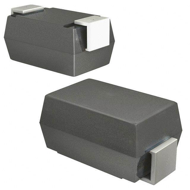
| 描述 | TVS DIODE 6VWM 15VC SOT23-6TVS二极管阵列 6V 0.1uA 20kV ESD Contact |
| 产品分类 | |
| 品牌 | Littelfuse Inc |
| 产品手册 | |
| 产品图片 |
|
| rohs | 符合RoHS无铅 / 符合限制有害物质指令(RoHS)规范要求 |
| 产品系列 | 二极管与整流器,TVS二极管,TVS二极管阵列,Littelfuse SRV05-4HTGSRV05, SPA® |
| 数据手册 | |
| 产品型号 | SRV05-4HTG |
| 不同频率时的电容 | - |
| 产品培训模块 | http://www.digikey.cn/PTM/IndividualPTM.page?site=cn&lang=zhs&ptm=22970http://www.digikey.cn/PTM/IndividualPTM.page?site=cn&lang=zhs&ptm=25590 |
| 产品种类 | TVS二极管阵列 |
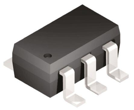
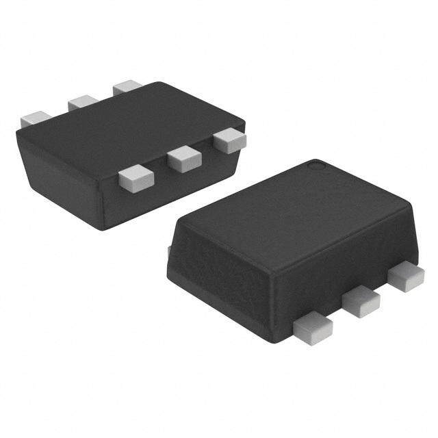
| 供应商器件封装 | SOT-23-6 |
| 其它名称 | F4204DKR |
| 功率-峰值脉冲 | 150W |
| 包装 | Digi-Reel® |
| 单向通道 | - |
| 双向通道 | 4 |
| 商标 | Littelfuse |
| 安装类型 | 表面贴装 |
| 安装风格 | SMD/SMT |
| 封装 | Reel |
| 封装/外壳 | SOT-23-6 |
| 封装/箱体 | SOT-23-6 |
| 尺寸 | 3 mm W x 3 mm L x 1.45 mm H |
| 峰值浪涌电流 | 10 A |
| 峰值脉冲功率耗散 | 150 W |
| 工作温度 | -40°C ~ 125°C (TJ) |
| 工作电压 | 6 V |
| 工厂包装数量 | 3000 |
| 应用 | 通用 |
| 最大工作温度 | + 85 C |
| 最小工作温度 | - 40 C |
| 极性 | Bidirectional |
| 标准包装 | 1 |
| 电压-击穿(最小值) | - |
| 电压-反向关态(典型值) | 6V (最小值) |
| 电压-箝位(最大值)@Ipp | 15V |
| 电流-峰值脉冲(10/1000µs) | 10A (8/20µs) |
| 电源线路保护 | 是 |
| 端接类型 | SMD/SMT |
| 类型 | 转向装置(轨至轨) |
| 系列 | SRV05 |
| 通道 | 4 Channels |
| 钳位电压 | 15 V |
| 零件号别名 | SP3050-04HTG |


- 商务部:美国ITC正式对集成电路等产品启动337调查
- 曝三星4nm工艺存在良率问题 高通将骁龙8 Gen1或转产台积电
- 太阳诱电将投资9.5亿元在常州建新厂生产MLCC 预计2023年完工
- 英特尔发布欧洲新工厂建设计划 深化IDM 2.0 战略
- 台积电先进制程称霸业界 有大客户加持明年业绩稳了
- 达到5530亿美元!SIA预计今年全球半导体销售额将创下新高
- 英特尔拟将自动驾驶子公司Mobileye上市 估值或超500亿美元
- 三星加码芯片和SET,合并消费电子和移动部门,撤换高东真等 CEO
- 三星电子宣布重大人事变动 还合并消费电子和移动部门
- 海关总署:前11个月进口集成电路产品价值2.52万亿元 增长14.8%

PDF Datasheet 数据手册内容提取
TVS Diode Arrays (SPA® Diodes) Low Capacitance ESD Protection - SRV05 Series SRV05 Series 6V 10A Diode Array RoHS Pb GREEN Description The SRV05 integrates low capacitance rail-to-rail diodes with an additional zener diode to protect each I/O pin against ESD and high surge events. This robust device can safely absorb surge current per IEC61000-4-5 (t =8/20µs) without P performance degradation and a minimum ±20kV ESD per IEC61000-4-2. Their very low loading capacitance also makes them ideal for protecting high speed signal pins. Features • E SD, IEC61000-4-2, • L ow capacitance of 2pF ±20kV contact, ±30kV air (TYP) per I/O • EFT, IEC61000-4-4, 40A • Low leakage current of Pinout (5/50ns) 0.5μA (MAX) at 5V • L ightning, IEC61000-4-5, • S mall SOT23-6 (JEDEC 10A (8/20μs) MO-178) packaging I/O 1 I/O 4 Applications GND V CC • LCD/PDP TVs • Firewire • Monitors • Set Top Boxes I/O 2 I/O 3 • Notebooks • Flat Panel Displays • 10/100/1000 Ethernet • Portable Medical Functional Block Diagram 10/100 Ethernet Differential Protection RJ45 ApplicaTtXi +on Examples Unused 6 5 4 10/100 UTTXnXu -+sed work EtPhHerYnetTX - USB DualR RPTTort ProtecStR12i3Vo0n5-4HTG6V54BUS DVD -B+US RXUP +oSrBt wisted-Pair Net ConUtSrRoXB l+ler CT CT VBUSSRV05-4HTG GND URnXu -sed To T Unused 75 75 75VBUS75 VRCXC - VCRCT VDB +US USB 1 2 3 GND RT D - Port CT CT GND Additional Information 10/100/1000 Ethernet Protection RJ45 Unused TX + Unused 10/100/1000 TTXX -+ work Datasheet Resources Samples EtPhHerYnetTX - 123 654 RX + wisted-Pair Net RX + SRV05-4HTG URnXu -sed To T Unused 75 75 75 75 RX - VCC Life Support Note: VCC Not Intended for Use in Life Support or Life Saving Applications GND The products shown herein are not designed for use in life sustaining or life saving applications unless otherwise expressly indicated. © 2017 Littelfuse, Inc. Specifications are subject to change without notice. Revised: 02/23/17
TVS Diode Arrays (SPA® Diodes) Low Capacitance ESD Protection - SRV05 Series Absolute Maximum Ratings Thermal Information Symbol Parameter Value Units Parameter Rating Units I Peak Current (t=8/20μs)1 10 A Storage Temperature Range –55 to 150 °C PP p Maximum Junction Temperature 150 °C P Peak Pulse Power (t=8/20μs) 150 W PK p Maximum Lead Temperature 260 °C T Operating Temperature –40 to 125 °C OP (Soldering 20-40s) T Storage Temperature –55 to 150 °C STOR CAUTION: Stresses above those listed in “Absolute Maximum Ratings” may cause permanent damage to the device. This is a stress only rating and operation of the device at these or any other conditions above those indicated in the operational sections of this specification is not implied. 1Non-repetitive pulse per waveform on page 3 Electrical Characteristics (T =25ºC) OP Parameter Symbol Test Conditions Min Typ Max Units Reverse Standoff Voltage V I ≤ 1µA 6.0 V RWM R Reverse Voltage Drop V I = 1mA 8.0 V R R Reverse Leakage Current I V =5V 0.1 0.5 µA LEAK R I =1A, t=8/20µs, I/O to GND2 8.8 10.0 V PP p Clamp Voltage1 V I =5A, t=8/20µs, I/O to GND2 11.5 13.0 V C PP p I =8A, t=8/20µs, I/O to GND2 13.2 15.0 V PP p Dynamic Resistance R (V - V ) / (I - I ) 0.7 Ω DYN C2 C1 PP2 PP1 IEC61000-4-2 (Contact) ±20 kV ESD Withstand Voltage1 V ESD IEC61000-4-2 (Air) ±30 kV Reverse Bias=0V 2.4 3.0 pF Diode Capacitance1 C I/O-GND Reverse Bias=1.65V 2.0 pF Diode Capacitance1 C Reverse Bias=0V 1.2 pF I/O-I/O Notes: 1 Parameter is guaranteed by design and/or device characterization. 2 Repetitive pulse per waveform on page 3. Clamping Voltage vs. I Product Characteristics PP 20.0 Lead Plating Matte Tin 18.0 Lead Material Copper Alloy 16.0 V)C 14.0 Lead Coplanarity 0.0004 inches (0.102mm) ge ( 12.0 Substitute Material Silicon a olt 10.0 p V 8.0 Body Material Molded Epoxy m Cla 6.0 Flammability UL 94 V-0 4.0 Notes : 2.0 1. All dimensions are in millimeters 0.0 2. Dimensions include solder plating. 1 2 3 4 5 6 7 8 9 10 3. Dimensions are exclusive of mold flash & metal burr. Peak Pulse Current-I (A) PP 4. Blo is facing up for mold and facing down for trim/form, i.e. reverse trim/form. 5. Package surface matte finish VDI 11-13. © 2017 Littelfuse, Inc. Specifications are subject to change without notice. Revised: 02/23/17
TVS Diode Arrays (SPA® Diodes) Low Capacitance ESD Protection - SRV05 Series Capacitance vs. Reverse Bias Pulse Waveform 3.0 110% 100% 2.5 90% VCC=Float 80% Capacitance (pF)112...050 VCC =3.3V VCC =5V Percent of IPP 45670000%%%% 30% 0.5 20% 10% 0.0 0% 0.0 0.5 1.0 1.5 2.0 2.5 3.0 3.5 4.0 4.5 5.0 0.0 5.0 10.0 15.0 20.0 25.0 30.0 DC Bias (V) Time (μs) Soldering Parameters Reflow Condition Pb – Free assembly tP TP CCrriittiiccaall ZZoonnee - Temperature Min (Ts(min)) 150°C e RRaammpp--uupp TTLL ttoo TTPP Pre Heat -- TTeimmep e(mraitnu rteo Mmaaxx )( T(ts()max)) 2600 0–° C180 secs rutare TS(mTaxL) tL s pm RRaammpp--ddoown Average ramp up rate (Liquidus) Temp e PPrreehheeaatt 3°C/second max T (TL) to peak TS(min) tS T to T - Ramp-up Rate 3°C/second max S(max) L Reflow -- TTeemmppeerraattuurree ((TtL)) (Liquidus) 26107 –° C1 50 seconds 25 time to peak temperature Time L Peak Temperature (T ) 260+0/-5 °C P Time within 5°C of actual peak 20 – 40 seconds Temperature (t ) p Ramp-down Rate 6°C/second max Time 25°C to peak Temperature (T ) 8 minutes Max. P Do not exceed 260°C Part Numbering System Part Marking System L*4 SRV05 – 4 H T G L*4 Product Series Number of Channels LL == SSRV05 G= Green Assembly Site T= Tape & Reel ((VVaarriieess)) Series Package Ordering Information Number of H: SOT23-6 Channels Part Number Package Marking Min. Order Qty. SRV05-4HTG SOT23-6 L*4 3000 © 2017 Littelfuse, Inc. Specifications are subject to change without notice. Revised: 02/23/17
TVS Diode Arrays (SPA® Diodes) Low Capacitance ESD Protection - SRV05 Series Package Dimensions — SOT23-6 Package SOT23-6 Pins 6 JEDEC MO-178 Millimeters Inches Notes Min Max Min Max A 0.900 1.450 0.035 0.057 - A1 0.000 0.150 0.000 0.006 - A2 0.900 1.300 0.035 0.051 - b 0.350 0.500 0.0138 0.0196 - C 0.080 0.220 0.0031 0.009 - D 2.800 3.000 0.11 0.118 3 E 2.600 3.000 0.102 0.118 - E1 1.500 1.750 0.06 0.069 3 e 0.95 Ref 0.0374 ref - e1 1.9 Ref 0.0748 Ref - L 0.100 0.600 0.004 0.023 4,5 N 6 6 6 Recommended Solder Pad Layout a 0º 10º 0º 10º - M 2.590 0.102 - O 0.690 .027 TYP - P 0.990 .039 TYP - M R 0.950 0.038 - Notes: 1. Dimensioning and tolerances per ANSI 14.5M-1982. 2. Package conforms to EIAJ SC-74 (1992). P 3. Dimensions D and E1 are exclusive of mold flash, protrusions, or gate burrs. 4. Footlenth L measured at reference to seating plane. 5. “L” is the length of flat foot surface for soldering to substrate. R 6. “N” is the number of terminal positions. 7. Controling dimension: MILLIMETER. Converted inch dimensions are not necessarily exact. O Embossed Carrier Tape & Reel Specification — SOT23-6 8mm TAPE AND REEL ACCESS HOLE DIA1..5 HmOmLE 4.0mm 2.0mm 1.75mm 14.4mm 8mm CL 4.0mm 13mm SOT-23 (8mm POCKET PITCH) GENERAL INFORMATION 1. 3000 PIECES PER REEL. 2. ORDER IN MULTIPLES OF FULL REELS ONLY. 180mm 60mm 3. MEETS EIA-481 REVISION "A" SPECIFICATIONS. 8.4mm USER DIRECTION OF FEED PIN 1 Disclaimer Notice - Information furnished is believed to be accurate and reliable. However, users should independently evaluate the suitability of and test each product selected for their own applications. Littelfuse products are not designed for, and may not be used in, all applications. Read complete Disclaimer Notice at www.littelfuse.com/disclaimer-electronics. © 2017 Littelfuse, Inc. Specifications are subject to change without notice. Revised: 02/23/17 COVER TAPE