 Datasheet下载
- 型号: SP1001-05JTG
- 制造商: Littelfuse
- 库位|库存: xxxx|xxxx
- 要求:
| 数量阶梯 | 香港交货 | 国内含税 |
| +xxxx | $xxxx | ¥xxxx |
查看当月历史价格
查看今年历史价格
SP1001-05JTG产品简介:
ICGOO电子元器件商城为您提供SP1001-05JTG由Littelfuse设计生产,在icgoo商城现货销售,并且可以通过原厂、代理商等渠道进行代购。 SP1001-05JTG价格参考¥1.73-¥3.50。LittelfuseSP1001-05JTG封装/规格:TVS - 二极管, 。您可以下载SP1001-05JTG参考资料、Datasheet数据手册功能说明书,资料中有SP1001-05JTG 详细功能的应用电路图电压和使用方法及教程。
Littelfuse Inc.的SP1001-05JTG是一款瞬态电压抑制(TVS)二极管,主要用于保护电子设备免受静电放电(ESD)、感应雷击和其它瞬态电压脉冲的损害。该型号的具体应用场景如下:

 1. 消费电子产品
   SP1001-05JTG广泛应用于各种消费类电子产品中,如智能手机、平板电脑、笔记本电脑等。它能够有效保护这些设备中的敏感电路,防止因静电或电源波动引起的损坏。例如,在手机的USB接口、耳机插孔、触摸屏等部位,SP1001-05JTG可以提供可靠的ESD保护,确保设备在日常使用中不会因为静电而出现故障。

 2. 通信设备
   在通信设备中,如路由器、调制解调器、交换机等,SP1001-05JTG用于保护网络接口、天线端口等关键部件。这些设备通常暴露在复杂的电磁环境中,容易受到雷击感应或电力波动的影响。通过安装SP1001-05JTG,可以有效抑制瞬态电压,确保通信系统的稳定性和可靠性。

 3. 工业自动化
   在工业自动化领域,SP1001-05JTG可用于保护传感器、控制器、PLC(可编程逻辑控制器)等设备。工业环境中的电气干扰较为严重,尤其是在存在大型电机、变频器等设备的情况下,瞬态电压可能会对控制系统造成损害。SP1001-05JTG能够迅速响应并抑制这些瞬态电压,确保工业设备的正常运行。

 4. 汽车电子
   汽车电子系统中,如车载信息娱乐系统、导航系统、车身控制模块等,也广泛应用了SP1001-05JTG。汽车内部的电气环境复杂,尤其是发动机启动时产生的瞬态电压可能对电子设备造成影响。SP1001-05JTG能够在这些场景下提供有效的保护,确保汽车电子系统的稳定性和安全性。

 5. 医疗设备
   医疗设备对可靠性的要求极高,任何瞬态电压都可能导致设备故障,进而影响患者的健康。SP1001-05JTG可用于保护心电图仪、监护仪、超声波设备等医疗仪器的关键电路,确保其在各种环境下都能正常工作。

总之,SP1001-05JTG凭借其快速响应时间和低箝位电压特性,成为众多电子设备中不可或缺的保护元件,适用于多种需要高可靠性和安全性的应用场景。
| 参数 | 数值 |
| 产品目录 | |
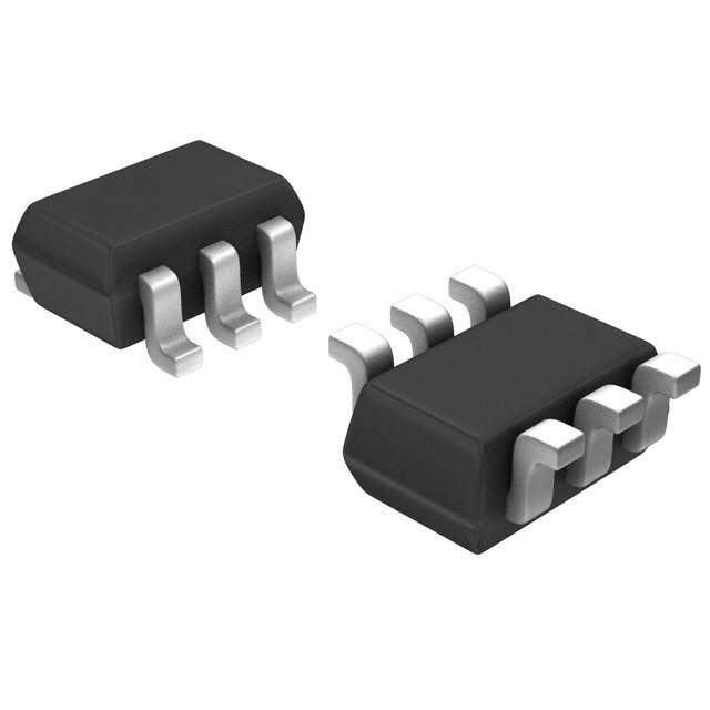
| 描述 | TVS DIODE 5.5VWM 13VC SC706TVS二极管阵列 5 channels |
| 产品分类 | |
| 品牌 | Littelfuse |
| 产品手册 | |
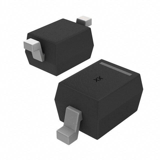
| 产品图片 |
|
| rohs | 符合RoHS无铅 / 符合限制有害物质指令(RoHS)规范要求 |
| 产品系列 | 二极管与整流器,TVS二极管,TVS二极管阵列,Littelfuse SP1001-05JTGSP1001, SPA® |
| 数据手册 | |
| 产品型号 | SP1001-05JTG |
| 不同频率时的电容 | - |
| 产品培训模块 | http://www.digikey.cn/PTM/IndividualPTM.page?site=cn&lang=zhs&ptm=22970http://www.digikey.cn/PTM/IndividualPTM.page?site=cn&lang=zhs&ptm=25590 |
| 产品目录绘图 |
|
| 产品目录页面 | |
| 产品种类 | TVS二极管阵列 |
| 供应商器件封装 | SC-70-6 |
| 其它名称 | F2897DKR |
| 击穿电压 | 5.5 V |
| 功率-峰值脉冲 | - |
| 包装 | Digi-Reel® |
| 单向通道 | 5 |
| 双向通道 | - |
| 商标 | Littelfuse |
| 商标名 | SPA |
| 安装类型 | 表面贴装 |
| 安装风格 | SMD/SMT |
| 封装 | Reel |
| 封装/外壳 | 6-TSSOP,SC-88,SOT-363 |
| 封装/箱体 | SC-70-6 |
| 尺寸 | 1.35 mm W x 2.25 mm L x 1 mm H |
| 峰值浪涌电流 | 2 A |
| 工作温度 | -40°C ~ 125°C (TJ) |
| 工作电压 | 5.5 V |
| 工厂包装数量 | 3000 |
| 应用 | 通用 |
| 最大工作温度 | + 85 C |
| 最小工作温度 | - 40 C |
| 极性 | Unidirectional |
| 标准包装 | 1 |
| 特色产品 | http://www.digikey.com/cn/zh/ph/Littelfuse/SP1000.html |
| 电压-击穿(最小值) | 7V |
| 电压-反向关态(典型值) | 5.5V(最小值) |
| 电压-箝位(最大值)@Ipp | 13V |
| 电容 | 8 pF |
| 电流-峰值脉冲(10/1000µs) | 2A (8/20µs) |
| 电源线路保护 | 无 |
| 端接类型 | SMD/SMT |
| 类型 | 齐纳 |
| 系列 | SP1001 |
| 通道 | 5 Channels |
| 钳位电压 | 9.7 V |


PDF Datasheet 数据手册内容提取
TVS Diode Arrays (SPA® Diodes) General Purpose ESD Protection - SP1001 Series SP1001 Series - 8pF 15kV Unidirectional TVS Array RoHS Pb GREEN Description Zener diodes fabricated in a proprietary silicon avalanche technology protect each I/O pin to provide a high level of protection for electronic equipment that may experience destructive electrostatic discharges (ESD). These robust diodes can safely absorb repetitive ESD strikes above the maximum level specified in the IEC 61000-4-2 international standard (Level 4, ±8kV contact discharge) without performance degradation. Their very low loading capacitance also makes them ideal for protecting high- speed signal pins. Features Pinout • Low capacitance of 8pF 0.5 to 0.1μA (MAX) at 5V (TYP) per I/O • Small package saves *SP1001-02 *SP1001-04 *SP1001-05 SP1001-02 • ESD protection of ±15kV board space (SC70-3) (SC70-5) (SC70-6) (SOT 553) 1 1 5 1 6 NC 5 contact discharge, ±30kV • Lightning protection, IEC air discharge, (Level 4, 61000-4-5, 2nd edition 2A 3 2 2 5 2 IEC 61000-4-2) (8/20µs) 2 3 4 3 4 NC 4 • EFT protection, IEC • AEC-Q101 qualified 61000-4-4, 40A (SC70-x packages) SP1001-04 SP1001-05 SP1001-05 (5/50ns) • RoHS compliant and lead- (SOT 553) (SOT 563) (SOT 963) • Low leakage current of free 1 5 1 6 1 6 2 2 5 2 5 Applications 3 4 3 4 3 4 • Computer Peripherals • LCD/PDP TVs *Note: AEC-Q101 qualified • Mobile Phones • Set Top Boxes • Digital Cameras • DVD Players Functional Block Diagram • Desktops/Notebooks • MP3/PMP SP1001-02 SP1001-02 1 2 5 4 Application Example Input LCD module Controller D1 3 2 D2 O D3 u ts D4 SP1001-04 SP1001-05 id 5 4 6 5 4 e W o r ld SP 1001-04JTG (SC70-5) SP 1001-04XTG (SOT553) Signal Shield Ground Ground 1 2 3 1 2 3 Additional Information Life Support Note: Not Intended for Use in Life Support or Life Saving Applications The products shown herein are not designed for use in life sustaining or life saving applications unless otherwise expressly indicated. Resources Samples © 2017 Littelfuse, Inc. Specifications are subject to change without notice. Revised: 05/12/17
TVS Diode Arrays (SPA® Diodes) General Purpose ESD Protection - SP1001 Series Absolute Maximum Ratings Thermal Information Symbol Parameter Value Units Parameter Rating Units I Peak Current (t=8/20μs) 2 A Storage Temperature Range –55 to 150 °C PP p TOP Operating Temperature –40 to 125 °C Maximum Junction Temperature 150 °C T Storage Temperature –55 to 150 °C STOR Maximum Lead Temperature (Soldering 260 °C 20s-40s) CAUTION: Stresses above those listed in “Absolute Maximum Ratings” may cause permanent damage to the device. This is a stress only rating and operation of the device at these or any other conditions above those indicated in the operational sections of this specification is not implied. Electrical Characteristics (T = 25°C) OP Parameter Symbol Test Conditions Min Typ Max Units Forward Voltage Drop V I=10mA 0.7 0.9 1.2 V F F Reverse Voltage Drop V I =1mA 6.0 8.5 V R R Reverse Standoff Voltage V I ≤1µA 5.5 V RWM R Reverse Leakage Current I V =5V 0.1 µA LEAK R I =1A, t=8/20µs, Fwd 8.0 11.0 V Clamp Voltage1 V PP p C I =2A, t=8/20µs, Fwd 9.7 13.0 V PP p Dynamic Resistance R (V - V ) / (I - I ) 1.7 Ω DYN C2 C1 PP2 PP1 IEC61000-4-2 (Contact) ±15 kV ESD Withstand Voltage1,2 V ESD IEC61000-4-2 (Air) ±30 kV Reverse Bias=0V 12 pF Diode Capacitance1 C Reverse Bias=2.5V 8 pF D Reverse Bias=5V 7 pF Notes: 1 Parameter is guaranteed by device characterization 2 A minimum of 1,000 ESD pulses are applied at 1s intervals between the anode and common cathode of each diode Capacitance vs. Reverse Bias Design Consideration Because of the fast rise-time of the ESD transient, 14 placement of ESD devices is a key design consideration. 12 To achieve optimal ESD suppression, the devices should be placed on the circuit board as close to the source of the ESD 10 transient as possible. Install the ESD suppressors directly pF) behind the connector so that they are the first board-level ce ( 8 circuit component encountered by the ESD transient. They n acita 6 are connected from signal/data line to ground. p a C 4 2 0 0 0.5 1 1.5 2 2.5 3 3.5 4 4.5 5 5.5 6 DC Bias (V) © 2017 Littelfuse, Inc. Specifications are subject to change without notice. Revised: 05/12/17
TVS Diode Arrays (SPA® Diodes) General Purpose ESD Protection - SP1001 Series Soldering Parameters Reflow Condition Pb – Free assembly - Temperature Min (T ) 150°C s(min) Pre Heat - Temperature Max (T ) 200°C s(max) - Time (min to max) (t) 60 – 180 secs s Average ramp up rate (Liquidus) Temp 3°C/second max (T) to peak L T to T - Ramp-up Rate 3°C/second max S(max) L - Temperature (T) (Liquidus) 217°C Reflow L - Temperature (t) 60 – 150 seconds L Peak Temperature (T ) 260+0/-5 °C P Time within 5°C of actual peak 20 – 40 seconds Temperature (t ) p Ramp-down Rate 6°C/second max Time 25°C to peak Temperature (T ) 8 minutes max. P Do not exceed 260°C Part Numbering System Product Characteristics SP1001- 0**TG Matte Tin (SC70-x) Pre-Plated Frame Lead Plating (SOT5x3, SOT963) TVS Diode Arrays (SPA® Diodes) G= Green Lead Material Copper Alloy T= Tape & Reel Package Lead Coplanarity 0.0004 inches (0.102mm) Series J = SC70-3, SC70-5 or SC70-6 Number of Channels X = SOT553 or SOT563 Substitute Silicon 02 = 2 Channel V = SOT963 Material 04 = 4 Channel 05 = 5 Channel Body Material Molded Epoxy Flammability UL 94 V-0 Part Marking System Notes : 1. All dimensions are in millimeters A* * 2. Dimensions include solder plating. 3. Dimensions are exclusive of mold flash & metal burr. A** Product Series Number of Channels 4. Blo is facing up for mold and facing down for trim/form, i.e. reverse trim/form. A = SP1001 series (varies) 5. Package surface matte finish VDI 11-13. Assembly Site (varies) Ordering Information Part Number Package Marking Min. Order Qty. SP1001-02JTG SC70-3 A*2 3000 SP1001-02XTG SOT553 A*2 3000 SP1001-04JTG SC70-5 A*4 3000 SP1001-04XTG SOT553 A*4 3000 SP1001-05JTG SC70-6 A*5 3000 SP1001-05VTG SOT963 A*5 8000 SP1001-05XTG SOT563 A*5 3000 © 2017 Littelfuse, Inc. Specifications are subject to change without notice. Revised: 05/12/17
TVS Diode Arrays (SPA® Diodes) General Purpose ESD Protection - SP1001 Series Package Dimensions — SC70 Package SC70-3 SC70-3 Pins 3 B Solder Pad Layout JEDEC MO-203 3 Millimeters Inches E HE Min Max Min Max A 0.80 1.10 0.031 0.043 1 2 e e A1 0.00 0.10 0.000 0.004 A2 0.70 1.00 0.028 0.039 D B 0.15 0.30 0.006 0.012 c 0.08 0.25 0.003 0.010 A2A D 1.85 2.25 0.073 0.089 A1 E 1.15 1.35 0.045 0.053 e 0.66 BSC 0.026 BSC C HE 2.00 2.40 0.079 0.094 L L 0.26 0.46 0.010 0.018 e e SC70-5 Package SC70-5 6 5 4 Solder Pad Layout Pins 5 not used JEDEC MO-203 E HE Millimeters Inches Min Max Min Max 1 2 3 A 0.80 1.10 0.031 0.043 B A1 0.00 0.10 0.000 0.004 A2 0.70 1.00 0.028 0.039 D B 0.15 0.30 0.006 0.012 A2 A c 0.08 0.25 0.003 0.010 D 1.85 2.25 0.073 0.089 A1 E 1.15 1.35 0.045 0.053 e 0.65 BSC 0.026 BSC C HE 2.00 2.40 0.079 0.094 L 0.26 0.46 0.010 0.018 L B B SC70-6 Package SC70-6 6 5 4 Solder Pad Layout Pins 6 JEDEC MO-203 E HE Millimeters Inches Min Max Min Max 1 2 3 A 0.80 1.10 0.031 0.043 B A1 0.00 0.10 0.000 0.004 D A2 0.70 1.00 0.028 0.039 B 0.15 0.30 0.006 0.012 A2A c 0.08 0.25 0.003 0.010 A1 D 1.85 2.25 0.073 0.089 E 1.15 1.35 0.045 0.053 C e 0.65 BSC 0.026 BSC HE 2.00 2.40 0.079 0.094 L L 0.26 0.46 0.010 0.018 © 2017 Littelfuse, Inc. Specifications are subject to change without notice. Revised: 05/12/17
TVS Diode Arrays (SPA® Diodes) General Purpose ESD Protection - SP1001 Series Package Dimensions — SOT553 and SOT563 A Package SOT 553 D L Pins 5 SOT 553 Millimeters Inches 6 (not 5used) 4 E HE Solder Pad Layout Min Max Min Max 2 3 A 0.50 0.60 0.020 0.024 B 0.17 0.27 0.007 0.011 e c c 0.08 0.18 0.003 0.007 B D 1.50 1.70 0.059 0.067 E 1.10 1.30 0.043 0.051 e 0.50 BSC 0.020 BSC L 0.10 0.30 0.004 0.012 HE 1.50 1.70 0.059 0.067 A Package SOT 563 D L SOT 563 Pins 6 6 5 4 Solder Pad Layout Millimeters Inches E HE Min Max Min Max 2 3 A 0.50 0.60 0.020 0.024 B 0.17 0.27 0.007 0.011 e c c 0.08 0.18 0.003 0.007 B D 1.50 1.70 0.059 0.067 E 1.10 1.30 0.043 0.051 e 0.50 BSC 0.020 BSC L 0.10 0.30 0.004 0.012 HE 1.50 1.70 0.059 0.067 Package Dimensions — SOT963 Package SOT 963 Pins 6 Millimeters Inches Min Nom Max Min Nom Max A 0.44 0.48 0.50 0.0173 0.0189 0.0197 B 0.10 0.15 0.20 0.004 0.006 0.008 c 0.05 0.10 0.15 0.002 0.004 0.006 D 0.95 1.00 1.05 0.037 0.039 0.041 E 0.75 0.80 0.85 0.029 0.031 0.033 E1 0.95 1.00 1.05 0.037 0.039 0.041 e 0.35 BSC 0.014 BSC L 0.05 0.10 0.15 0.002 0.004 0.006 L1 0.125 0.15 0.175 0.005 0.006 0.007 ø 3 º 5 º 7 º 3 º 5 º 7 º Recommanded Solder Pad Layout © 2017 Littelfuse, Inc. Specifications are subject to change without notice. Revised: 05/12/17
TVS Diode Arrays (SPA® Diodes) General Purpose ESD Protection - SP1001 Series Embossed Carrier Tape & Reel Specification — SC70-3 Dimensions Millimetres Inches Min Max Min Max E 1.65 1.85 0.065 0.073 F 3.45 3.55 0.135 0.139 P2 1.95 2.05 0.077 0.081 D 1.40 1.60 0.055 0.063 D1 1.00 1.25 0.039 0.049 P0 3.90 4.10 0.154 0.161 10P0 40.0 ± 0.20 1.574 ± 0.008 W 7.70 8.10 0.303 0.318 P 3.90 4.10 0.153 0.161 A0 2.30 2.50 0.090 0.098 A1 1.00 Ref 0.039 Ref B0 2.30 2.50 0.090 0.098 B1 1.90 Ref 0.074 K0 1.10 1.30 0.043 0.051 K1 0.60 Ref 0.023 Ref t 0.27 max 0.010 Embossed Carrier Tape & Reel Specification — SC70-5 and SC70-6 Dimensions Millimetres Inches Min Max Min Max E 1.65 1.85 0.065 0.073 F 3.45 3.55 0.135 0.139 P2 1.95 2.05 0.077 0.081 D 1.40 1.60 0.055 0.063 D1 1.00 1.25 0.039 0.049 P0 3.90 4.10 0.154 0.161 10P0 40.0 ± 0.20 1.574 ± 0.008 W 7.70 8.10 0.303 0.318 P 3.90 4.10 0.153 0.161 A0 2.14 2.34 0.084 0.092 B0 2.24 2.44 0.088 0.096 K0 1.12 1.32 0.044 0.052 t 0.27 max 0.010 max © 2017 Littelfuse, Inc. Specifications are subject to change without notice. Revised: 05/12/17
TVS Diode Arrays (SPA® Diodes) General Purpose ESD Protection - SP1001 Series Embossed Carrier Tape & Reel Specification — SOT553 and SOT563 Dimensions Millimetres Inches Min Max Min Max E 1.65 1.85 0.065 0.073 F 3.45 3.55 0.135 0.139 P2 1.95 2.05 0.077 0.081 D 1.40 1.60 0.055 0.063 D1 0.45 0.55 0.017 0.021 P0 3.90 4.1 0.154 0.161 10P0 40.0 ± 0.20 1.574 ± 0.008 W 7.70 8.10 0.303 0.318 P 3.90 4.10 0.153 0.161 A0 1.73 1.83 0.068 0.072 B0 1.73 1.83 0.068 0.072 K0 0.64 0.74 0.025 0.029 t 0.22 max .009 max Embossed Carrier Tape & Reel Specification – SOT963 PO D P2 /o t Dimensions Millimetres Inches Symbol E Min Max Min Max E 1.65 1.85 0.065 0.073 W F 3.45 3.55 0.136 0.140 D1 0.45 0.55 0.018 0.022 F D 1.50 min 0.059 min P0 3.90 4.10 0.154 0.161 o/D1 O 10P0 40.0 ± 0.20 1.575 ± 0.008 P B P 1.95 2.05 0.077 0.081 AO P2 1.95 2.05 0.077 0.081 W 7.90 8.20 0.311 0.323 A0 1.11 1.21 0.044 0.048 B0 1.11 1.21 0.044 0.048 K0 0.58 0.68 0.023 0.027 O K t 0.22 max 0.009 max Disclaimer Notice - Information furnished is believed to be accurate and reliable. However, users should independently evaluate the suitability of and test each product selected for their own applications. Littelfuse products are not designed for, and may not be used in, all applications. Read complete Disclaimer Notice at www.littelfuse.com/disclaimer-electronics. © 2017 Littelfuse, Inc. Specifications are subject to change without notice. Revised: 05/12/17