ICGOO在线商城 > 集成电路(IC) > 逻辑 - 缓冲器,驱动器,接收器,收发器 > SN74LVTH244ADW
 Datasheet下载
- 型号: SN74LVTH244ADW
- 制造商: Texas Instruments
- 库位|库存: xxxx|xxxx
- 要求:
| 数量阶梯 | 香港交货 | 国内含税 |
| +xxxx | $xxxx | ¥xxxx |
查看当月历史价格
查看今年历史价格
SN74LVTH244ADW产品简介:
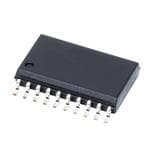
ICGOO电子元器件商城为您提供SN74LVTH244ADW由Texas Instruments设计生产,在icgoo商城现货销售,并且可以通过原厂、代理商等渠道进行代购。 SN74LVTH244ADW价格参考¥3.31-¥4.63。Texas InstrumentsSN74LVTH244ADW封装/规格:逻辑 - 缓冲器,驱动器,接收器,收发器, Buffer, Non-Inverting 2 Element 4 Bit per Element 3-State Output 20-SOIC。您可以下载SN74LVTH244ADW参考资料、Datasheet数据手册功能说明书,资料中有SN74LVTH244ADW 详细功能的应用电路图电压和使用方法及教程。
SN74LVTH244ADW 是 Texas Instruments 生产的一款逻辑缓冲器/驱动器芯片,属于 SN74LVTH 系列。它主要应用于需要信号缓冲、电平转换或驱动能力增强的场景。以下是其典型应用场景:

 1. 数据总线缓冲
   - SN74LVTH244ADW 可用于计算机系统或嵌入式设备中的数据总线缓冲。它支持 8 位并行数据传输,能够将输入信号进行缓冲后输出,从而避免信号在长距离传输或复杂电路中衰减。
   - 适用于多主从设备通信场景,例如扩展微控制器或 FPGA 的数据总线。

 2. 信号驱动增强
   - 在需要驱动高负载(如 LED 阵列、继电器或其他外设)的应用中,该芯片可以增强信号的驱动能力。它具有较高的输出电流能力,确保信号能够可靠地驱动外部设备。

 3. 电平转换
   - 由于支持不同的电压范围(1.65V 至 5.5V),SN74LVTH244ADW 可用于不同电压逻辑电路之间的电平转换。例如,在低功耗 MCU(3.3V)与传统外围设备(5V)之间实现兼容性。

 4. 多路信号隔离
   - 在复杂的数字系统中,多个信号可能需要独立控制和隔离。SN74LVTH244ADW 提供了方向控制引脚(G 和 /G),可以通过使能/禁用功能选择性地传递信号,避免信号干扰。

 5. 存储器接口扩展
   - 在设计带有扩展存储器的系统时,该芯片可以用作地址或数据总线的缓冲器,以提高系统的稳定性和可靠性。

 6. 工业控制与通信
   - 在工业自动化领域,SN74LVTH244ADW 可用于 PLC、数据采集模块或通信接口中,作为信号调理或驱动元件,确保信号的完整性和抗干扰能力。

 7. 消费电子设备
   - 在家用电器、显示面板或音频设备中,该芯片可用于驱动显示屏、键盘矩阵或其他外设接口,提供稳定的信号输出。

 总结
SN74LVTH244ADW 的主要优势在于其高集成度、宽电压范围和较强的驱动能力,适合用于需要信号缓冲、驱动增强或电平转换的各种数字电路中。它广泛应用于计算机、通信、工业控制和消费电子等领域。
| 参数 | 数值 |
| 产品目录 | 集成电路 (IC)半导体 |
| 描述 | IC BUFF/DVR TRI-ST DUAL 20SOIC缓冲器和线路驱动器 Tri-State ABT Octal |
| 产品分类 | |
| 品牌 | Texas Instruments |
| 产品手册 | |
| 产品图片 |
|
| rohs | 符合RoHS无铅 / 符合限制有害物质指令(RoHS)规范要求 |
| 产品系列 | 逻辑集成电路,缓冲器和线路驱动器,Texas Instruments SN74LVTH244ADW74LVTH |
| 数据手册 | |
| 产品型号 | SN74LVTH244ADW |
| 产品目录页面 | |
| 产品种类 | 缓冲器和线路驱动器 |
| 传播延迟时间 | 2.3 ns at 3.3 V |
| 低电平输出电流 | 64 mA |
| 供应商器件封装 | 20-SOIC |
| 元件数 | 2 |
| 其它名称 | 296-1270-5 |
| 包装 | 管件 |
| 单位重量 | 500.700 mg |
| 商标 | Texas Instruments |
| 安装类型 | 表面贴装 |
| 安装风格 | SMD/SMT |
| 封装 | Tube |
| 封装/外壳 | 20-SOIC(0.295",7.50mm 宽) |
| 封装/箱体 | SOIC-20 |
| 工作温度 | -40°C ~ 85°C |
| 工厂包装数量 | 25 |
| 最大工作温度 | + 85 C |
| 最小工作温度 | - 40 C |
| 极性 | Non-Inverting |
| 标准包装 | 25 |
| 每元件位数 | 4 |
| 每芯片的通道数量 | 8 |
| 电压-电源 | 2.7 V ~ 3.6 V |
| 电流-输出高,低 | 32mA,64mA |
| 电源电压-最大 | 3.6 V |
| 电源电压-最小 | 2.7 V |
| 电源电流 | 0.005 mA |
| 系列 | SN74LVTH244A |
| 输入线路数量 | 8 |
| 输出类型 | 3-State |
| 输出线路数量 | 3 |
| 逻辑类型 | 缓冲器/线路驱动器,非反相 |
| 逻辑系列 | LVT |
| 高电平输出电流 | - 32 mA |


- 商务部:美国ITC正式对集成电路等产品启动337调查
- 曝三星4nm工艺存在良率问题 高通将骁龙8 Gen1或转产台积电
- 太阳诱电将投资9.5亿元在常州建新厂生产MLCC 预计2023年完工
- 英特尔发布欧洲新工厂建设计划 深化IDM 2.0 战略
- 台积电先进制程称霸业界 有大客户加持明年业绩稳了
- 达到5530亿美元!SIA预计今年全球半导体销售额将创下新高
- 英特尔拟将自动驾驶子公司Mobileye上市 估值或超500亿美元
- 三星加码芯片和SET,合并消费电子和移动部门,撤换高东真等 CEO
- 三星电子宣布重大人事变动 还合并消费电子和移动部门
- 海关总署:前11个月进口集成电路产品价值2.52万亿元 增长14.8%


PDF Datasheet 数据手册内容提取
SN54LVTH244A, SN74LVTH244A 3.3-V ABT OCTAL BUFFERS/DRIVERS WITH 3-STATE OUTPUTS SCAS586J − DECEMBER 1996 − REVISED OCTOBER 2003 (cid:2) (cid:2) Support Mixed-Mode Signal Operation (5-V Bus Hold on Data Inputs Eliminates the Input and Output Voltages With 3.3-V V ) Need for External Pullup/Pulldown CC (cid:2) Typical V (Output Ground Bounce) Resistors OLP <0.8 V at V = 3.3 V, T = 25°C (cid:2) Latch-Up Performance Exceeds 500 mA Per CC A (cid:2) Support Unregulated Battery Operation JESD 17 (cid:2) Down to 2.7 V ESD Protection Exceeds JESD 22 (cid:2) − 2000-V Human-Body Model (A114-A) I and Power-Up 3-State Support Hot off − 200-V Machine Model (A115-A) Insertion SN54LVTH244A...J OR W PACKAGE SN74LVTH244A...RGY PACKAGE SN54LVTH244A...FK PACKAGE SN74LVTH244A...DB, DW, NS, (TOP VIEW) (TOP VIEW) OR PW PACKAGE (TOP VIEW) OE CC Y4 A1 OE CCOE 1 V 2 1 1V 2 1OE 1 20 VCC 1 20 3 2 1 20 19 1A1 2 19 2OE 1A1 2 19 2OE 1A2 4 18 1Y1 2Y4 3 18 1Y1 2Y4 3 18 1Y1 2Y3 5 17 2A4 1A2 4 17 2A4 1A2 4 17 2A4 1A3 6 16 1Y2 2Y3 5 16 1Y2 2Y3 5 16 1Y2 2Y2 7 15 2A3 1A3 6 15 2A3 1A3 6 15 2A3 1A4 8 14 1Y3 2Y2 7 14 1Y3 2Y2 7 14 1Y3 9 10 11 12 13 1A4 8 13 2A2 1A4 8 13 2A2 1 D 14 2 2Y1 9 12 1Y4 Y N AY A 2Y1 9 12 1Y4 2 G 21 2 GND 10 11 2A1 10 11 D 1 N A G 2 description/ordering information These octal buffers and line drivers are designed specifically for low-voltage (3.3-V) V operation, but with the CC capability to provide a TTL interface to a 5-V system environment. ORDERING INFORMATION ORDERABLE TA PACKAGE† PART NUMBER TOP-SIDE MARKING QFN − RGY Tape and reel SN74LVTH244ARGYR LXH244A Tube SN74LVTH244ADW SSOOIICC − DDWW LLVVTTHH224444AA Tape and reel SN74LVTH244ADWR SOP − NS Tape and reel SN74LVTH244ANSR LVTH244A −4400°°CC ttoo 8855°°CC SSOP − DB Tape and reel SN74LVTH244ADBR LXH244A TSSOP − PW Tape and reel SN74LVTH244APWR LXH244A VFBGA − GQN SN74LVTH244AGQNR TTaappee aanndd rreeeell LLXXHH224444AA VFBGA − ZQN (Pb-free) SN74LVTH244AZQNR CDIP − J Tube SNJ54LVTH244AJ SNJ54LVTH244AJ −55°C to 125°C CFP − W Tube SNJ54LVTH244AW SNJ54LVTH244AW LCCC − FK Tube SNJ54LVTH244AFK SNJ54LVTH244AFK †Package drawings, standard packing quantities, thermal data, symbolization, and PCB design guidelines are available at www.ti.com/sc/package. Please be aware that an important notice concerning availability, standard warranty, and use in critical applications of TexasInstruments semiconductor products and disclaimers thereto appears at the end of this data sheet. PRODUCTION DATA information is current as of publication date. Copyright © 2003, Texas Instruments Incorporated Products conform to specifications per the terms of Texas Instruments On products compliant to MIL-PRF-38535, all parameters are tested standard warranty. Production processing does not necessarily include unless otherwise noted. On all other products, production testing of all parameters. processing does not necessarily include testing of all parameters. POST OFFICE BOX 655303 • DALLAS, TEXAS 75265 1
SN54LVTH244A, SN74LVTH244A 3.3-V ABT OCTAL BUFFERS/DRIVERS WITH 3-STATE OUTPUTS SCAS586J − DECEMBER 1996 − REVISED OCTOBER 2003 description/ordering information (continued) The ’LVTH244A devices are organized as two 4-bit line drivers with separate output-enable (OE) inputs. When OE is low, the devices pass data from the A inputs to the Y outputs. When OE is high, the outputs are in the high-impedance state. To ensure the high-impedance state during power up or power down, OE should be tied to V through a pullup CC resistor; the minimum value of the resistor is determined by the current-sinking capability of the driver. Active bus-hold circuitry is provided to hold unused or floating data inputs at a valid logic level. Use of pullup or pulldown resistors with the bus-hold circuitry is not recommended. These devices are fully specified for hot-insertion applications using I and power-up 3-state. The I circuitry off off disables the outputs, preventing damaging current backflow through the devices when they are powered down. The power-up 3-state circuitry places the outputs in the high-impedance state during power up and power down, which prevents driver conflict. SN74LVTH244A...GQN OR ZQN PACKAGE (TOP VIEW) terminal assignments 1 2 3 4 1 2 3 4 A A 1A1 1OE VCC 2OE B B 1A2 2A4 2Y4 1Y1 C C 1A3 2Y3 2A3 1Y2 D D 1A4 2A2 2Y2 1Y3 E GND 2Y1 2A1 1Y4 E FUNCTION TABLE (each buffer) INPUTS OOUUTTPPUUTT OE A Y L H H L L L H X Z 2 POST OFFICE BOX 655303 • DALLAS, TEXAS 75265
SN54LVTH244A, SN74LVTH244A 3.3-V ABT OCTAL BUFFERS/DRIVERS WITH 3-STATE OUTPUTS SCAS586J − DECEMBER 1996 − REVISED OCTOBER 2003 logic diagram (positive logic) 1 19 1OE 2OE 2 18 11 9 1A1 1Y1 2A1 2Y1 4 16 13 7 1A2 1Y2 2A2 2Y2 6 14 15 5 1A3 1Y3 2A3 2Y3 8 12 17 3 1A4 1Y4 2A4 2Y4 Pin numbers shown are for the DB, DW, FK, J, NS, PW, RGY, and W packages. absolute maximum ratings over operating free-air temperature range (unless otherwise noted)† Supply voltage range, V . . . . . . . . . . . . . . . . . . . . . . . . . . . . . . . . . . . . . . . . . . . . . . . . . . . . . . . . . −0.5 V to 4.6 V CC Input voltage range, V (see Note 1) . . . . . . . . . . . . . . . . . . . . . . . . . . . . . . . . . . . . . . . . . . . . . . . . . . −0.5 V to 7 V I Voltage range applied to any output in the high-impedance or power-off state, VO (see Note 1) . . . . . . . . . . . . . . . . . . . . . . . . . . . . . . . . . . . . . . . . . . . . . . . . . −0.5 V to 7 V Voltage range applied to any output in the high state, VO (see Note 1) . . . . . . . . . . . . . −0.5 V to VCC + 0.5 V Current into any output in the low state, I : SN54LVTH244A . . . . . . . . . . . . . . . . . . . . . . . . . . . . . . . . . . 96 mA O SN74LVTH244A . . . . . . . . . . . . . . . . . . . . . . . . . . . . . . . . . 128 mA Current into any output in the high state, IO (see Note 2): SN54LVTH244A . . . . . . . . . . . . . . . . . . . . . . 48 mA SN74LVTH244A . . . . . . . . . . . . . . . . . . . . . . 64 mA Input clamp current, IIK (VI < 0) . . . . . . . . . . . . . . . . . . . . . . . . . . . . . . . . . . . . . . . . . . . . . . . . . . . . . . . . . . . −50 mA Output clamp current, IOK (VO < 0) . . . . . . . . . . . . . . . . . . . . . . . . . . . . . . . . . . . . . . . . . . . . . . . . . . . . . . . . −50 mA Package thermal impedance, θJA (see Note 3): DB package . . . . . . . . . . . . . . . . . . . . . . . . . . . . . . . . . 70°C/W (see Note 3): DW package . . . . . . . . . . . . . . . . . . . . . . . . . . . . . . . . . 58°C/W (see Note 3): GQN/ZQN package . . . . . . . . . . . . . . . . . . . . . . . . . . . 78°C/W (see Note 3): NS package . . . . . . . . . . . . . . . . . . . . . . . . . . . . . . . . . 60°C/W (see Note 3): PW package . . . . . . . . . . . . . . . . . . . . . . . . . . . . . . . . . 83°C/W (see Note 4): RGY package . . . . . . . . . . . . . . . . . . . . . . . . . . . . . . . . 37°C/W Storage temperature range, T . . . . . . . . . . . . . . . . . . . . . . . . . . . . . . . . . . . . . . . . . . . . . . . . . . . −65°C to 150°C stg †Stresses beyond those listed under “absolute maximum ratings” may cause permanent damage to the device. These are stress ratings only, and functional operation of the device at these or any other conditions beyond those indicated under “recommended operating conditions” is not implied. Exposure to absolute-maximum-rated conditions for extended periods may affect device reliability. NOTES: 1. The input and output negative-voltage ratings may be exceeded if the input and output clamp-current ratings are observed. 2. This current flows only when the output is in the high state and VO > VCC. 3. The package thermal impedance is calculated in accordance with JESD 51-7. 4. The package thermal impedance is calculated in accordance with JESD 51-5. POST OFFICE BOX 655303 • DALLAS, TEXAS 75265 3
SN54LVTH244A, SN74LVTH244A 3.3-V ABT OCTAL BUFFERS/DRIVERS WITH 3-STATE OUTPUTS SCAS586J − DECEMBER 1996 − REVISED OCTOBER 2003 recommended operating conditions (see Note 5) SN54LVTH244A SN74LVTH244A UUNNIITT MIN MAX MIN MAX VCC Supply voltage 2.7 3.6 2.7 3.6 V VIH High-level input voltage 2 2 V VIL Low-level input voltage 0.8 0.8 V VI Input voltage 5.5 5.5 V IOH High-level output current −24 −32 mA IOL Low-level output current 48 64 mA Δt/Δv Input transition rise or fall rate Outputs enabled 10 10 ns/V Δt/ΔVCC Power-up ramp rate 200 200 μs/V TA Operating free-air temperature −55 125 −40 85 °C NOTE 5: All unused control inputs of the device must be held at VCC or GND to ensure proper device operation. Refer to the TI application report, Implications of Slow or Floating CMOS Inputs, literature number SCBA004. 4 POST OFFICE BOX 655303 • DALLAS, TEXAS 75265
SN54LVTH244A, SN74LVTH244A 3.3-V ABT OCTAL BUFFERS/DRIVERS WITH 3-STATE OUTPUTS SCAS586J − DECEMBER 1996 − REVISED OCTOBER 2003 electrical characteristics over recommended operating free-air temperature range (unless otherwise noted) SN54LVTH244A SN74LVTH244A PPAARRAAMMEETTEERR TTEESSTT CCOONNDDIITTIIOONNSS UUNNIITT MIN TYP† MAX MIN TYP† MAX VIK VCC = 2.7 V, II = −18 mA −1.2 −1.2 V VCC = 2.7 V to 3.6 V, IOH = −100 μA VCC−0.2 VCC−0.2 VCC = 2.7 V, IOH = −8 mA 2.4 2.4 VVOH IOH = −24 mA 2 VV VVCC = 33 VV IOH = −32 mA 2 IOL = 100 μA 0.2 0.2 VVCC = 22.77 VV IOL = 24 mA 0.5 0.5 IOL = 16 mA 0.4 0.4 VVOL IOL = 32 mA 0.5 0.5 VV VVCC = 33 VV IOL = 48 mA 0.55 IOL = 64 mA 0.55 VCC = 0 or 3.6 V, VI = 5.5 V 50 10 CCoonnttrrooll iinnppuuttss VCC = 3.6 V, VI = VCC or GND ±1 ±1 III VI = VCC 1 1 μAA DDaattaa iinnppuuttss VVCC = 33.66 VV VI = 0 −5 −5 Ioff VCC = 0, VI or VO = 0 to 4.5 V ±100 μA VI = 0.8 V 75 75 IIII((hholldd)) DDaattaa iinnppuuttss VVCC = 33 VV VI = 2 V −75 −75 μμAA 500 VCC = 3.6 V‡, VI = 0 to 3.6 V −750 IOZH VCC = 3.6 V, VO = 3 V 5 5 μA IOZL VCC = 3.6 V, VO = 0.5 V −5 −5 μA IOZPU VOCEC = = d 0o nto’t 1c.a5r eV, VO = 0.5 V to 3 V, ±100∗ ±100 μA IOZPD VOCEC = = d 1o.n5’ tV c atore 0, VO = 0.5 V to 3 V, ±100∗ ±100 μA Outputs high 0.39 0.19 VVCCCC == 33..66 VV,, IICCCC IIOO = 00,, Outputs low 14 5 mmAA VI = VCC or GND Outputs disabled 0.39 0.19 ΔICC§ VOCthCe =r i3n pVu ttso a3t. 6V CVC, O onr eG iNnpDut at VCC − 0.6 V, 0.2 0.2 mA Ci VI = 3 V or 0 3 3 pF Co VO = 3 V or 0 7 7 pF ∗ On products compliant to MIL-PRF-38535, this parameter is not production tested. †All typical values are at VCC = 3.3 V, TA = 25°C. ‡This is the bus-hold maximum dynamic current. It is the minimum overdrive current required to switch the input from one state to another. §This is the increase in supply current for each input that is at the specified TTL voltage level, rather than VCC or GND. POST OFFICE BOX 655303 • DALLAS, TEXAS 75265 5
SN54LVTH244A, SN74LVTH244A 3.3-V ABT OCTAL BUFFERS/DRIVERS WITH 3-STATE OUTPUTS SCAS586J − DECEMBER 1996 − REVISED OCTOBER 2003 switching characteristics over recommended operating free-air temperature range, C = 50 pF L (unless otherwise noted) (see Figure 1) SN54LVTH244A SN74LVTH244A PARAMETER ((IIFNNRPPOUUMTT)) ((OOUUTTTOPPUUTT)) VC±C 0=. 33 .V3 V VCC = 2.7 V VC±C 0=. 33 .V3 V VCC = 2.7 V UNIT MIN MAX MIN MAX MIN TYP† MAX MIN MAX tPLH 0.5 3.8 4.1 1.1 2.3 3.5 3.8 AA YY nnss tPHL 0.5 3.8 3.9 1.3 2.1 3.3 3.6 tPZH 0.8 5 6 1.1 2.5 4.5 5.3 OOEE YY nnss tPZL 0.8 5 5.4 1.4 2.7 4.4 4.9 tPHZ 1.3 5.5 5.8 1.9 2.8 4.4 4.5 OOEE YY nnss tPLZ 1.2 4.7 4.8 1.8 2.9 4.4 4.4 †All typical values are at VCC = 3.3 V, TA = 25°C. 6 POST OFFICE BOX 655303 • DALLAS, TEXAS 75265
SN54LVTH244A, SN74LVTH244A 3.3-V ABT OCTAL BUFFERS/DRIVERS WITH 3-STATE OUTPUTS SCAS586J − DECEMBER 1996 − REVISED OCTOBER 2003 PARAMETER MEASUREMENT INFORMATION 6 V TEST S1 500 Ω S1 Open From Output tPLH/tPHL Open Under Test GND tPLZ/tPZL 6 V CL = 50 pF 500 Ω tPHZ/tPZH GND (see Note A) 2.7 V LOAD CIRCUIT Timing Input 1.5 V 0 V tw tsu th 2.7 V 2.7 V Input 1.5 V 1.5 V Data Input 1.5 V 1.5 V 0 V 0 V VOLTAGE WAVEFORMS VOLTAGE WAVEFORMS PULSE DURATION SETUP AND HOLD TIMES 2.7 V 2.7 V Output Input 1.5 V 1.5 V 1.5 V 1.5 V Control 0 V 0 V tPLH tPHL tPZL tPLZ VOH Output 3 V Output 1.5 V 1.5 V VOL (WseaeSv eN1f ooatrte m6 B V1) 1.5 V VOL + 0.3 V VOL tPHL tPLH tPZH tPHZ Output Output 1.5 V 1.5 V VOH WSa1v eafto GrmN D2 1.5 V VOH − 0.3 V VOH VOL (see Note B) ≈0 V VOLTAGE WAVEFORMS VOLTAGE WAVEFORMS PROPAGATION DELAY TIMES ENABLE AND DISABLE TIMES INVERTING AND NONINVERTING OUTPUTS LOW- AND HIGH-LEVEL ENABLING NOTES: A. CL includes probe and jig capacitance. B. Waveform 1 is for an output with internal conditions such that the output is low except when disabled by the output control. Waveform2 is for an output with internal conditions such that the output is high except when disabled by the output control. C. All input pulses are supplied by generators having the following characteristics: PRR ≤ 10 MHz, ZO = 50 Ω, tr ≤ 2.5 ns, tf≤ 2.5 ns. D. The outputs are measured one at a time with one transition per measurement. E. All parameters and waveforms are not applicable to all devices. Figure 1. Load Circuit and Voltage Waveforms POST OFFICE BOX 655303 • DALLAS, TEXAS 75265 7
PACKAGE OPTION ADDENDUM www.ti.com 24-Aug-2018 PACKAGING INFORMATION Orderable Device Status Package Type Package Pins Package Eco Plan Lead/Ball Finish MSL Peak Temp Op Temp (°C) Device Marking Samples (1) Drawing Qty (2) (6) (3) (4/5) 5962-9584401Q2A ACTIVE LCCC FK 20 1 TBD POST-PLATE N / A for Pkg Type -55 to 125 5962- 9584401Q2A SNJ54LVTH 244AFK 5962-9584401QRA ACTIVE CDIP J 20 1 TBD A42 N / A for Pkg Type -55 to 125 5962-9584401QR A SNJ54LVTH244AJ 5962-9584401QSA ACTIVE CFP W 20 1 TBD A42 N / A for Pkg Type -55 to 125 5962-9584401QS A SNJ54LVTH244AW 5962-9584401V2A ACTIVE LCCC FK 20 1 TBD POST-PLATE N / A for Pkg Type -55 to 125 5962- 9584401V2A SNV54LVTH 244AFK 5962-9584401VRA ACTIVE CDIP J 20 1 TBD A42 N / A for Pkg Type -55 to 125 5962-9584401VR A SNV54LVTH244AJ 5962-9584401VSA ACTIVE CFP W 20 1 TBD A42 N / A for Pkg Type -55 to 125 5962-9584401VS A SNV54LVTH244AW SN74LVTH244ADB ACTIVE SSOP DB 20 70 Green (RoHS CU NIPDAU Level-1-260C-UNLIM LXH244A & no Sb/Br) SN74LVTH244ADBR ACTIVE SSOP DB 20 2000 Green (RoHS CU NIPDAU Level-1-260C-UNLIM -40 to 85 LXH244A & no Sb/Br) SN74LVTH244ADBRE4 ACTIVE SSOP DB 20 2000 Green (RoHS CU NIPDAU Level-1-260C-UNLIM -40 to 85 LXH244A & no Sb/Br) SN74LVTH244ADBRG4 ACTIVE SSOP DB 20 2000 Green (RoHS CU NIPDAU Level-1-260C-UNLIM -40 to 85 LXH244A & no Sb/Br) SN74LVTH244ADW ACTIVE SOIC DW 20 25 Green (RoHS CU NIPDAU Level-1-260C-UNLIM -40 to 85 LVTH244A & no Sb/Br) SN74LVTH244ADWE4 ACTIVE SOIC DW 20 25 Green (RoHS CU NIPDAU Level-1-260C-UNLIM -40 to 85 LVTH244A & no Sb/Br) SN74LVTH244ADWG4 ACTIVE SOIC DW 20 25 Green (RoHS CU NIPDAU Level-1-260C-UNLIM -40 to 85 LVTH244A & no Sb/Br) Addendum-Page 1
PACKAGE OPTION ADDENDUM www.ti.com 24-Aug-2018 Orderable Device Status Package Type Package Pins Package Eco Plan Lead/Ball Finish MSL Peak Temp Op Temp (°C) Device Marking Samples (1) Drawing Qty (2) (6) (3) (4/5) SN74LVTH244ADWR ACTIVE SOIC DW 20 2000 Green (RoHS CU NIPDAU Level-1-260C-UNLIM -40 to 85 LVTH244A & no Sb/Br) SN74LVTH244ADWRG4 ACTIVE SOIC DW 20 2000 Green (RoHS CU NIPDAU Level-1-260C-UNLIM -40 to 85 LVTH244A & no Sb/Br) SN74LVTH244ANSR ACTIVE SO NS 20 2000 Green (RoHS CU NIPDAU Level-1-260C-UNLIM -40 to 85 LVTH244A & no Sb/Br) SN74LVTH244APW ACTIVE TSSOP PW 20 70 Green (RoHS CU NIPDAU Level-1-260C-UNLIM -40 to 85 LXH244A & no Sb/Br) SN74LVTH244APWG4 ACTIVE TSSOP PW 20 70 Green (RoHS CU NIPDAU Level-1-260C-UNLIM -40 to 85 LXH244A & no Sb/Br) SN74LVTH244APWR ACTIVE TSSOP PW 20 2000 Green (RoHS CU NIPDAU | CU SN Level-1-260C-UNLIM -40 to 85 LXH244A & no Sb/Br) SN74LVTH244APWRE4 ACTIVE TSSOP PW 20 2000 Green (RoHS CU NIPDAU Level-1-260C-UNLIM -40 to 85 LXH244A & no Sb/Br) SN74LVTH244APWRG4 ACTIVE TSSOP PW 20 2000 Green (RoHS CU NIPDAU Level-1-260C-UNLIM -40 to 85 LXH244A & no Sb/Br) SN74LVTH244ARGYR ACTIVE VQFN RGY 20 3000 Green (RoHS CU NIPDAU Level-2-260C-1 YEAR -40 to 85 LXH244A & no Sb/Br) SN74LVTH244AZQNR ACTIVE BGA ZQN 20 1000 Green (RoHS SNAGCU Level-1-260C-UNLIM -40 to 85 LXH244A MICROSTAR & no Sb/Br) JUNIOR SNJ54LVTH244AFK ACTIVE LCCC FK 20 1 TBD POST-PLATE N / A for Pkg Type -55 to 125 5962- 9584401Q2A SNJ54LVTH 244AFK SNJ54LVTH244AJ ACTIVE CDIP J 20 1 TBD A42 N / A for Pkg Type -55 to 125 5962-9584401QR A SNJ54LVTH244AJ SNJ54LVTH244AW ACTIVE CFP W 20 1 TBD A42 N / A for Pkg Type -55 to 125 5962-9584401QS A SNJ54LVTH244AW (1) The marketing status values are defined as follows: ACTIVE: Product device recommended for new designs. LIFEBUY: TI has announced that the device will be discontinued, and a lifetime-buy period is in effect. NRND: Not recommended for new designs. Device is in production to support existing customers, but TI does not recommend using this part in a new design. PREVIEW: Device has been announced but is not in production. Samples may or may not be available. OBSOLETE: TI has discontinued the production of the device. Addendum-Page 2
PACKAGE OPTION ADDENDUM www.ti.com 24-Aug-2018 (2) RoHS: TI defines "RoHS" to mean semiconductor products that are compliant with the current EU RoHS requirements for all 10 RoHS substances, including the requirement that RoHS substance do not exceed 0.1% by weight in homogeneous materials. Where designed to be soldered at high temperatures, "RoHS" products are suitable for use in specified lead-free processes. TI may reference these types of products as "Pb-Free". RoHS Exempt: TI defines "RoHS Exempt" to mean products that contain lead but are compliant with EU RoHS pursuant to a specific EU RoHS exemption. Green: TI defines "Green" to mean the content of Chlorine (Cl) and Bromine (Br) based flame retardants meet JS709B low halogen requirements of <=1000ppm threshold. Antimony trioxide based flame retardants must also meet the <=1000ppm threshold requirement. (3) MSL, Peak Temp. - The Moisture Sensitivity Level rating according to the JEDEC industry standard classifications, and peak solder temperature. (4) There may be additional marking, which relates to the logo, the lot trace code information, or the environmental category on the device. (5) Multiple Device Markings will be inside parentheses. Only one Device Marking contained in parentheses and separated by a "~" will appear on a device. If a line is indented then it is a continuation of the previous line and the two combined represent the entire Device Marking for that device. (6) Lead/Ball Finish - Orderable Devices may have multiple material finish options. Finish options are separated by a vertical ruled line. Lead/Ball Finish values may wrap to two lines if the finish value exceeds the maximum column width. Important Information and Disclaimer:The information provided on this page represents TI's knowledge and belief as of the date that it is provided. TI bases its knowledge and belief on information provided by third parties, and makes no representation or warranty as to the accuracy of such information. Efforts are underway to better integrate information from third parties. TI has taken and continues to take reasonable steps to provide representative and accurate information but may not have conducted destructive testing or chemical analysis on incoming materials and chemicals. TI and TI suppliers consider certain information to be proprietary, and thus CAS numbers and other limited information may not be available for release. In no event shall TI's liability arising out of such information exceed the total purchase price of the TI part(s) at issue in this document sold by TI to Customer on an annual basis. OTHER QUALIFIED VERSIONS OF SN54LVTH244A, SN54LVTH244A-SP, SN74LVTH244A : •Catalog: SN74LVTH244A, SN54LVTH244A •Enhanced Product: SN74LVTH244A-EP, SN74LVTH244A-EP •Military: SN54LVTH244A •Space: SN54LVTH244A-SP NOTE: Qualified Version Definitions: •Catalog - TI's standard catalog product Addendum-Page 3
PACKAGE OPTION ADDENDUM www.ti.com 24-Aug-2018 •Enhanced Product - Supports Defense, Aerospace and Medical Applications •Military - QML certified for Military and Defense Applications •Space - Radiation tolerant, ceramic packaging and qualified for use in Space-based application Addendum-Page 4
PACKAGE MATERIALS INFORMATION www.ti.com 12-Feb-2019 TAPE AND REEL INFORMATION *Alldimensionsarenominal Device Package Package Pins SPQ Reel Reel A0 B0 K0 P1 W Pin1 Type Drawing Diameter Width (mm) (mm) (mm) (mm) (mm) Quadrant (mm) W1(mm) SN74LVTH244ADBR SSOP DB 20 2000 330.0 16.4 8.2 7.5 2.5 12.0 16.0 Q1 SN74LVTH244ADWR SOIC DW 20 2000 330.0 24.4 10.8 13.3 2.7 12.0 24.0 Q1 SN74LVTH244ANSR SO NS 20 2000 330.0 24.4 8.4 13.0 2.5 12.0 24.0 Q1 SN74LVTH244APWR TSSOP PW 20 2000 330.0 16.4 6.95 7.1 1.6 8.0 16.0 Q1 SN74LVTH244ARGYR VQFN RGY 20 3000 330.0 12.4 3.8 4.8 1.6 8.0 12.0 Q1 SN74LVTH244AZQNR BGAMI ZQN 20 1000 330.0 12.4 3.3 4.3 1.6 8.0 12.0 Q1 CROSTA RJUNI OR PackMaterials-Page1
PACKAGE MATERIALS INFORMATION www.ti.com 12-Feb-2019 *Alldimensionsarenominal Device PackageType PackageDrawing Pins SPQ Length(mm) Width(mm) Height(mm) SN74LVTH244ADBR SSOP DB 20 2000 367.0 367.0 38.0 SN74LVTH244ADWR SOIC DW 20 2000 367.0 367.0 45.0 SN74LVTH244ANSR SO NS 20 2000 367.0 367.0 45.0 SN74LVTH244APWR TSSOP PW 20 2000 364.0 364.0 27.0 SN74LVTH244ARGYR VQFN RGY 20 3000 367.0 367.0 35.0 SN74LVTH244AZQNR BGAMICROSTAR ZQN 20 1000 350.0 350.0 43.0 JUNIOR PackMaterials-Page2
None
None
None
None
None
PACKAGE OUTLINE DB0020A TSSOP - 2 mm max height SCALE 2.000 SMALL OUTLINE PACKAGE C 8.2 TYP 7.4 A 0.1 C PIN 1 INDEX AREA SEATING PLANE 18X 0.65 20 1 2X 7.5 5.85 6.9 NOTE 3 10 11 0.38 20X 0.22 5.6 B 0.1 C A B 5.0 NOTE 4 2 MAX (0.15) TYP 0.25 SEE DETAIL A GAGE PLANE 0 -8 0.95 0.05 MIN 0.55 DETA 15AIL A TYPICAL 4214851/A 12/2017 NOTES: 1. All linear dimensions are in millimeters. Any dimensions in parenthesis are for reference only. Dimensioning and tolerancing per ASME Y14.5M. 2. This drawing is subject to change without notice. 3. This dimension does not include mold flash, protrusions, or gate burrs. Mold flash, protrusions, or gate burrs shall not exceed 0.15 mm per side. 4. This dimension does not include interlead flash. Interlead flash shall not exceed 0.25 mm per side. 5. Reference JEDEC registration MO-150. www.ti.com
EXAMPLE BOARD LAYOUT DB0020A TSSOP - 2 mm max height SMALL OUTLINE PACKAGE 20X (1.85) SYMM (R0.05) TYP 1 20X (0.45) 20 SYMM 18X (0.65) 10 11 (7) LAND PATTERN EXAMPLE EXPOSED METAL SHOWN SCALE: 10X SOLDER MASK METAL METAL UNDER SOLDER MASK OPENING SOLDER MASK OPENING EXPOSED METAL EXPOSED METAL 0.07 MAX 0.07 MIN ALL AROUND ALL AROUND NON-SOLDER MASK SOLDER MASK DEFINED DEFINED (PREFERRED) SOLDE15.000 R MASK DETAILS 4214851/A 12/2017 NOTES: (continued) 6. Publication IPC-7351 may have alternate designs. 7. Solder mask tolerances between and around signal pads can vary based on board fabrication site. www.ti.com
EXAMPLE STENCIL DESIGN DB0020A TSSOP - 2 mm max height SMALL OUTLINE PACKAGE 20X (1.85) SYMM (R0.05) TYP 1 20X (0.45) 20 SYMM 18X (0.65) 10 11 (7) SOLDER PASTE EXAMPLE BASED ON 0.125 mm THICK STENCIL SCALE: 10X 4214851/A 12/2017 NOTES: (continued) 8. Laser cutting apertures with trapezoidal walls and rounded corners may offer better paste release. IPC-7525 may have alternate design recommendations. 9. Board assembly site may have different recommendations for stencil design. www.ti.com
PACKAGE OUTLINE DW0020A SOIC - 2.65 mm max height SCALE 1.200 SOIC C 10.63 SEATING PLANE TYP 9.97 A PIN 1 ID 0.1 C AREA 18X 1.27 20 1 13.0 2X 12.6 11.43 NOTE 3 10 11 0.51 20X 7.6 0.31 2.65 MAX B 7.4 0.25 C A B NOTE 4 0.33 TYP 0.10 0.25 SEE DETAIL A GAGE PLANE 0.3 1.27 0 - 8 0.1 0.40 DETAIL A TYPICAL 4220724/A 05/2016 NOTES: 1. All linear dimensions are in millimeters. Dimensions in parenthesis are for reference only. Dimensioning and tolerancing per ASME Y14.5M. 2. This drawing is subject to change without notice. 3. This dimension does not include mold flash, protrusions, or gate burrs. Mold flash, protrusions, or gate burrs shall not exceed 0.15 mm per side. 4. This dimension does not include interlead flash. Interlead flash shall not exceed 0.43 mm per side. 5. Reference JEDEC registration MS-013. www.ti.com
EXAMPLE BOARD LAYOUT DW0020A SOIC - 2.65 mm max height SOIC 20X (2) SYMM 1 20 20X (0.6) 18X (1.27) SYMM (R0.05) TYP 10 11 (9.3) LAND PATTERN EXAMPLE SCALE:6X SOOPLEDNEINRG MASK METAL MSOELTDAEL RU NMDAESRK SOOPLEDNEINRG MASK 0.07 MAX 0.07 MIN ALL AROUND ALL AROUND NON SOLDER MASK SOLDER MASK DEFINED DEFINED SOLDER MASK DETAILS 4220724/A 05/2016 NOTES: (continued) 6. Publication IPC-7351 may have alternate designs. 7. Solder mask tolerances between and around signal pads can vary based on board fabrication site. www.ti.com
EXAMPLE STENCIL DESIGN DW0020A SOIC - 2.65 mm max height SOIC 20X (2) SYMM 1 20 20X (0.6) 18X (1.27) SYMM 10 11 (9.3) SOLDER PASTE EXAMPLE BASED ON 0.125 mm THICK STENCIL SCALE:6X 4220724/A 05/2016 NOTES: (continued) 8. Laser cutting apertures with trapezoidal walls and rounded corners may offer better paste release. IPC-7525 may have alternate design recommendations. 9. Board assembly site may have different recommendations for stencil design. www.ti.com
None
None
None
None
None
IMPORTANTNOTICEANDDISCLAIMER TIPROVIDESTECHNICALANDRELIABILITYDATA(INCLUDINGDATASHEETS),DESIGNRESOURCES(INCLUDINGREFERENCE DESIGNS),APPLICATIONOROTHERDESIGNADVICE,WEBTOOLS,SAFETYINFORMATION,ANDOTHERRESOURCES“ASIS” ANDWITHALLFAULTS,ANDDISCLAIMSALLWARRANTIES,EXPRESSANDIMPLIED,INCLUDINGWITHOUTLIMITATIONANY IMPLIEDWARRANTIESOFMERCHANTABILITY,FITNESSFORAPARTICULARPURPOSEORNON-INFRINGEMENTOFTHIRD PARTYINTELLECTUALPROPERTYRIGHTS. TheseresourcesareintendedforskilleddevelopersdesigningwithTIproducts.Youaresolelyresponsiblefor(1)selectingtheappropriate TIproductsforyourapplication,(2)designing,validatingandtestingyourapplication,and(3)ensuringyourapplicationmeetsapplicable standards,andanyothersafety,security,orotherrequirements.Theseresourcesaresubjecttochangewithoutnotice.TIgrantsyou permissiontousetheseresourcesonlyfordevelopmentofanapplicationthatusestheTIproductsdescribedintheresource.Other reproductionanddisplayoftheseresourcesisprohibited.NolicenseisgrantedtoanyotherTIintellectualpropertyrightortoanythird partyintellectualpropertyright.TIdisclaimsresponsibilityfor,andyouwillfullyindemnifyTIanditsrepresentativesagainst,anyclaims, damages,costs,losses,andliabilitiesarisingoutofyouruseoftheseresources. TI’sproductsareprovidedsubjecttoTI’sTermsofSale(www.ti.com/legal/termsofsale.html)orotherapplicabletermsavailableeitheron ti.comorprovidedinconjunctionwithsuchTIproducts.TI’sprovisionoftheseresourcesdoesnotexpandorotherwisealterTI’sapplicable warrantiesorwarrantydisclaimersforTIproducts. MailingAddress:TexasInstruments,PostOfficeBox655303,Dallas,Texas75265 Copyright©2019,TexasInstrumentsIncorporated