ICGOO在线商城 > 集成电路(IC) > 逻辑 - 缓冲器,驱动器,接收器,收发器 > 74LCX245WM

 Datasheet下载
- 型号: 74LCX245WM
- 制造商: Fairchild Semiconductor
- 库位|库存: xxxx|xxxx
- 要求:
| 数量阶梯 | 香港交货 | 国内含税 |
| +xxxx | $xxxx | ¥xxxx |
查看当月历史价格
查看今年历史价格
74LCX245WM产品简介:
ICGOO电子元器件商城为您提供74LCX245WM由Fairchild Semiconductor设计生产,在icgoo商城现货销售,并且可以通过原厂、代理商等渠道进行代购。 74LCX245WM价格参考¥询价-¥询价。Fairchild Semiconductor74LCX245WM封装/规格:逻辑 - 缓冲器,驱动器,接收器,收发器, Transceiver, Non-Inverting 1 Element 8 Bit per Element 3-State Output 20-SOIC。您可以下载74LCX245WM参考资料、Datasheet数据手册功能说明书,资料中有74LCX245WM 详细功能的应用电路图电压和使用方法及教程。
ON Semiconductor的74LCX245WM是一款高性能、低功耗的8位总线收发器,属于逻辑 - 缓冲器、驱动器、接收器和收发器类别。该器件广泛应用于需要高效数据传输和信号转换的场景中,特别适合于计算机系统、通信设备、工业控制和其他需要高速数据处理的应用。

 主要应用场景:

1. 计算机系统:
   74LCX245WM常用于计算机主板、扩展卡和外设接口中,用于实现不同总线之间的数据传输。它可以在CPU、内存和其他外围设备之间提供高效的双向数据传输,确保数据的完整性和可靠性。例如,在PCI、ISA等总线接口中,该芯片可以作为数据缓冲器和收发器,提高系统的稳定性和性能。

2. 通信设备:
   在网络通信设备中,如路由器、交换机和调制解调器,74LCX245WM用于管理和转换数据信号。它可以有效地隔离不同的信号路径,防止信号干扰,并确保数据在不同速率和协议下的正确传输。此外,该芯片还支持热插拔功能,使得在网络设备中进行模块化设计时更加灵活。

3. 工业控制系统:
   在工业自动化和控制系统中,74LCX245WM用于连接各种传感器、执行器和控制器。它可以处理来自不同设备的数据流,确保信号的准确传递。例如,在PLC(可编程逻辑控制器)中,该芯片可以帮助实现输入输出信号的转换和管理,提高系统的响应速度和精度。

4. 消费电子:
   在一些高端消费电子产品中,如智能电视、游戏主机和多媒体播放器,74LCX245WM用于实现内部组件之间的高效数据传输。它能够处理高带宽的数据流,确保视频、音频和其他多媒体内容的流畅播放。

5. 测试与测量设备:
   在测试仪器和测量设备中,74LCX245WM用于连接不同的测试模块和接口。它能够确保数据的实时传输和精确采集,适用于示波器、频谱分析仪等精密仪器。

总之,74LCX245WM凭借其低功耗、高速度和高可靠性,成为多种应用场景中不可或缺的关键元件,特别是在需要高效数据传输和信号转换的场合。
| 参数 | 数值 |
| 产品目录 | 集成电路 (IC)半导体 |
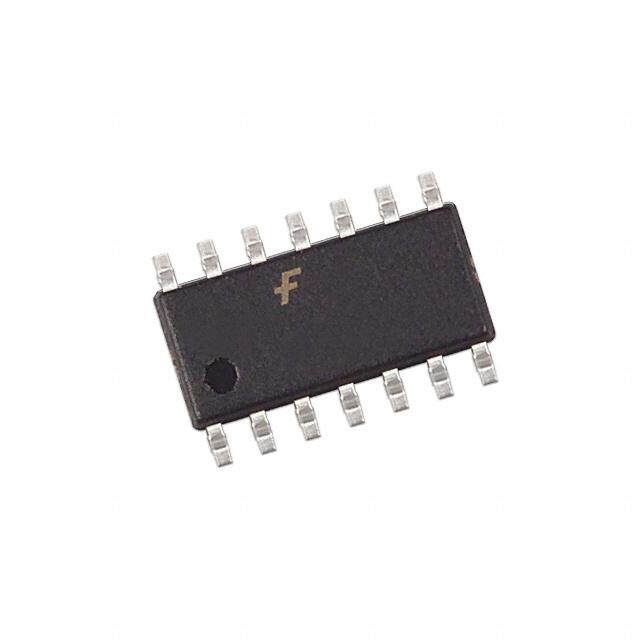
| 描述 | IC TRANSCVR BIDIR 8BIT 20SOIC总线收发器 Bidirectional Trans |
| 产品分类 | |
| 品牌 | Fairchild Semiconductor |
| 产品手册 | |
| 产品图片 |
|
| rohs | 符合RoHS无铅 / 符合限制有害物质指令(RoHS)规范要求 |
| 产品系列 | 逻辑集成电路,总线收发器,Fairchild Semiconductor 74LCX245WM74LCX |
| 数据手册 | |
| 产品型号 | 74LCX245WM |
| 产品目录页面 | |
| 产品种类 | 总线收发器 |
| 传播延迟时间 | 8 ns |
| 低电平输出电流 | 24 mA |
| 供应商器件封装 | 20-SOIC |
| 元件数 | 1 |
| 功能 | Transceiver |
| 包装 | 管件 |
| 单位重量 | 801 mg |
| 商标 | Fairchild Semiconductor |
| 安装类型 | 表面贴装 |
| 安装风格 | SMD/SMT |
| 封装 | Tube |
| 封装/外壳 | 20-SOIC(0.295",7.50mm 宽) |
| 封装/箱体 | SOIC-20 |
| 工作温度 | -40°C ~ 85°C |
| 工厂包装数量 | 36 |
| 最大工作温度 | + 85 C |
| 最小工作温度 | - 40 C |
| 极性 | Non-Inverting |
| 标准包装 | 36 |
| 每元件位数 | 8 |
| 每芯片的通道数量 | 8 |
| 电压-电源 | 2 V ~ 3.6 V |
| 电流-输出高,低 | 24mA,24mA |
| 电源电压-最大 | 3.6 V |
| 电源电压-最小 | 2 V |
| 电路数量 | 1 |
| 系列 | 74LCX245 |
| 输入电平 | LVTTL, TTL |
| 输出电平 | LVCMOS |
| 输出类型 | 3-State |
| 逻辑类型 | CMOS |
| 逻辑系列 | 74LCX |
| 零件号别名 | 74LCX245WM_NL |
| 高电平输出电流 | - 24 mA |


- 商务部:美国ITC正式对集成电路等产品启动337调查
- 曝三星4nm工艺存在良率问题 高通将骁龙8 Gen1或转产台积电
- 太阳诱电将投资9.5亿元在常州建新厂生产MLCC 预计2023年完工
- 英特尔发布欧洲新工厂建设计划 深化IDM 2.0 战略
- 台积电先进制程称霸业界 有大客户加持明年业绩稳了
- 达到5530亿美元!SIA预计今年全球半导体销售额将创下新高
- 英特尔拟将自动驾驶子公司Mobileye上市 估值或超500亿美元
- 三星加码芯片和SET,合并消费电子和移动部门,撤换高东真等 CEO
- 三星电子宣布重大人事变动 还合并消费电子和移动部门
- 海关总署:前11个月进口集成电路产品价值2.52万亿元 增长14.8%


PDF Datasheet 数据手册内容提取
Is Now Part of To learn more about ON Semiconductor, please visit our website at www.onsemi.com Please note: As part of the Fairchild Semiconductor integration, some of the Fairchild orderable part numbers will need to change in order to meet ON Semiconductor’s system requirements. Since the ON Semiconductor product management systems do not have the ability to manage part nomenclature that utilizes an underscore (_), the underscore (_) in the Fairchild part numbers will be changed to a dash (-). This document may contain device numbers with an underscore (_). Please check the ON Semiconductor website to verify the updated device numbers. The most current and up-to-date ordering information can be found at www.onsemi.com. Please email any questions regarding the system integration to Fairchild_questions@onsemi.com. ON Semiconductor and the ON Semiconductor logo are trademarks of Semiconductor Components Industries, LLC dba ON Semiconductor or its subsidiaries in the United States and/or other countries. ON Semiconductor owns the rights to a number of patents, trademarks, copyrights, trade secrets, and other intellectual property. A listing of ON Semiconductor’s product/patent coverage may be accessed at www.onsemi.com/site/pdf/Patent-Marking.pdf. ON Semiconductor reserves the right to make changes without further notice to any products herein. ON Semiconductor makes no warranty, representation or guarantee regarding the suitability of its products for any particular purpose, nor does ON Semiconductor assume any liability arising out of the application or use of any product or circuit, and specifically disclaims any and all liability, including without limitation special, consequential or incidental damages. Buyer is responsible for its products and applications using ON Semiconductor products, including compliance with all laws, regulations and safety requirements or standards, regardless of any support or applications information provided by ON Semiconductor. “Typical” parameters which may be provided in ON Semiconductor data sheets and/or specifications can and do vary in different applications and actual performance may vary over time. All operating parameters, including “Typicals” must be validated for each customer application by customer’s technical experts. ON Semiconductor does not convey any license under its patent rights nor the rights of others. ON Semiconductor products are not designed, intended, or authorized for use as a critical component in life support systems or any FDA Class 3 medical devices or medical devices with a same or similar classification in a foreign jurisdiction or any devices intended for implantation in the human body. Should Buyer purchase or use ON Semiconductor products for any such unintended or unauthorized application, Buyer shall indemnify and hold ON Semiconductor and its officers, employees, subsidiaries, affiliates, and distributors harmless against all claims, costs, damages, and expenses, and reasonable attorney fees arising out of, directly or indirectly, any claim of personal injury or death associated with such unintended or unauthorized use, even if such claim alleges that ON Semiconductor was negligent regarding the design or manufacture of the part. ON Semiconductor is an Equal Opportunity/Affirmative Action Employer. This literature is subject to all applicable copyright laws and is not for resale in any manner.
7 4 L C X December 2013 2 4 5 — 74LCX245 L o Low Voltage Bidirectional Transceiver with 5V Tolerant w V o Inputs and Outputs l t a g e Features General Description B i d ■ 5V tolerant inputs and outputs The LCX245 contains eight non-inverting bidirectional i r ■ 2.3V to 3.6V V specifications provided buffers with 3-STATE outputs and is intended for bus e CC c ■ 7.0ns tPD max. (VCC = 3.3V), 10µA ICC max. ovoriletangteed ( 2a.p5pVl icaantdio 3n.s3.V T) hVe d eavpipcleic aisti odness wiginthe dc afpoar bliolitwy tio ■ Power down high impedance inputs and outputs CC n of interfacing to a 5V signal environment. The T/R input a ■ Supports live insertion/withdrawal(1) determines the direction of data flow through the device. l T ■ ±24mA output drive (VCC = 3.0V) The OE input disables both the A and B ports by placing ra ■ Implements proprietary noise/EMI reduction circuitry them in a high impedance state. n s ■ Latch-up performance exceeds 500mA The LCX245 is fabricated with an advanced CMOS tech- c e ■ ESD performance: nology to achieve high speed operation while maintain- i v – Human body model > 2000V ing CMOS low power dissipation. e r – Machine model > 200V w i ■ Leadless DQFN package th 5 V Note: T 1. To ensure the high-impedance state during power up o l or down, OE should be tied to V through a pull-up e CC r resistor: the minimum value or the resistor is a n determined by the current-sourcing capability of the t driver. In p u t s Ordering Information a n d Package O Order Number Number Package Description u t p 74LCX245WM M20B 20-Lead Small Outline Integrated Circuit (SOIC), JEDEC MS-013, 0.300" Wide u t s 74LCX245SJ M20D 20-Lead Small Outline Package (SOP), EIAJ TYPE II, 5.3mm Wide 74LCX245BQX(2) MLP20B 20-Terminal Depopulated Quad Very-Thin Flat Pack No Leads (DQFN), JEDEC MO-241, 2.5 x 4.5mm 74LCX245MSA MSA20 20-Lead Shrink Small Outline Package (SSOP), JEDEC MO-150, 5.3mm Wide 74LCX245MTC MTC20 20-Lead Thin Shrink Small Outline Package (TSSOP), JEDEC MO-153, 4.4mm Wide Note: 2. DQFN package available in Tape and Reel only. Device also available in Tape and Reel. Specify by appending suffix letter “X” to the ordering number. All packages are lead free per JEDEC: J-STD-020B standard. ©1994 Fairchild Semiconductor Corporation www.fairchildsemi.com 74LCX245 Rev. 1.11.1
7 4 Connection Diagrams Logic Symbol L C X Pin Assignments for SOIC, SOP, SSOP, and TSSOP 2 4 5 — L o w V o l t a g e Truth Table B i d Inputs ir e c OE T/R Outputs t i o L L Bus B – B Data to Bus A – A n 0 7 0 7 a L H Bus A0 – A7 Data to Bus B0 – B7 l T r Pin Assignment for DQFN H X HIGH Z State on A – A , B – B (3) a 0 7 0 7 n s H = HIGH Voltage Level c e L = LOW Voltage Level i v X = Immaterial e r Z = High Impedance w i t h Note: 5 3. Unused bus terminals during HIGH Z State must be V held HIGH or LOW. T o l e r a Logic Diagram n t I n p u t s a n d O (Top Through View) (Bottom View) u t p u t s Pin Description Pin Description Names OE Output Enable Input T/R Transmit/Receive Input A –A Side A Inputs or 3-STATE Outputs 0 7 B –B Side B Inputs or 3-STATE Outputs 0 7 DAP No Connect Note: DAP (Die Attach Pad) ©1994 Fairchild Semiconductor Corporation www.fairchildsemi.com 74LCX245 Rev. 1.11.1 2
7 4 Absolute Maximum Ratings L C Stresses exceeding the absolute maximum ratings may damage the device. The device may not function or be X 2 operable above the recommended operating conditions and stressing the parts to these levels is not recommended. 4 In addition, extended exposure to stresses above the recommended operating conditions may affect device reliability. 5 The absolute maximum ratings are stress ratings only. — L Symbol Parameter Rating o w VCC Supply Voltage –0.5V to +7.0V V V DC Input Voltage –0.5V to +7.0V o I l t V DC Output Voltage a O g e Output in 3-STATE –0.5V to +7.0V B Output in HIGH or LOW State(4) –0.5V to V + 0.5V i CC d I DC Input Diode Current, V < GND –50mA ir IK I e c IOK DC Output Diode Current ti V < GND –50mA o O n VO > VCC +50mA al T I DC Output Source/Sink Current ±50mA r O a n ICC DC Supply Current per Supply Pin ±100mA s c IGND DC Ground Current per Ground Pin ±100mA e i v TSTG Storage Temperature –65°C to +150°C e r Note: w i 4. I Absolute Maximum Rating must be observed. t O h 5 V Recommended Operating Conditions(5) T o The Recommended Operating Conditions table defines the conditions for actual device operation. Recommended le r operating conditions are specified to ensure optimal performance to the datasheet specifications. Fairchild does not a n recommend exceeding them or designing to absolute maximum ratings. t I n Symbol Parameter Min. Max. Units p u VCC Supply Voltage ts Operating 2.0 3.6 V a n Data Retention 1.5 3.6 d V Input Voltage 0 5.5 V O I u VO Output Voltage tp u 3-STATE 0 5.5 V t s HIGH or LOW State 0 V CC IOH / IOL Output Current V = 3.0V–3.6V ±24 mA CC V = 2.7V–3.0V ±12 CC V = 2.3V–2.7V ±8 CC T Free-Air Operating Temperature –40 85 °C A ∆t / ∆V Input Edge Rate, VIN = 0.8V–2.0V, VCC = 3.0V 0 10 ns / V Note: 5. Unused inputs must be held HIGH or LOW. They may not float. ©1994 Fairchild Semiconductor Corporation www.fairchildsemi.com 74LCX245 Rev. 1.11.1 3
7 4 DC Electrical Characteristics L C X TA = –40°C to +85°C 2 4 Symbol Parameter V (V) Conditions Min. Max. Units 5 CC — V HIGH Level Input Voltage 2.3–2.7 1.7 V IH L 2.7–3.6 2.0 o w VIL LOW Level Input Voltage 2.3–2.7 0.7 V V o 2.7–3.6 0.8 l t VOH HIGH Level Output Voltage 2.3–3.6 IOH = –100µA VCC – 0.2 V ag e 2.3 IOH = –8mA 1.8 B 2.7 IOH = –12mA 2.2 id i 3.0 IOH = –18mA 2.4 re c I = –24mA 2.2 t OH i o V LOW Level Output Voltage 2.3–3.6 I = 100µA 0.2 V n OL OL a 2.3 IOL = 8mA 0.6 l T 2.7 IOL = 12mA 0.4 ra n 3.0 I = 16mA 0.4 s OL c I = 24mA 0.55 e OL i v I Input Leakage Current 2.3–3.6 0 ≤ V ≤ 5.5V ±5.0 µA e I I r I 3-STATE Output Leakage 2.3–3.6 0 ≤ V ≤ 5.5V, ±5.0 µA w OZ O VI = VIH or VIL ith IOFF Power-Off Leakage Current 0 VI or VO = 5.5V 10 µA 5 V ICC Quiescent Supply Current 2.3–3.6 VI = VCC or GND 10 µA T o 3.6V ≤ VI, VO ≤ 5.5V(6) ±10 le ∆ICC Increase in ICC per Input 2.3–3.6 VIH = VCC – 0.6V 500 µA ra n Note: t I n 6. Outputs disabled or 3-STATE only. p u t s AC Electrical Characteristics a n d T = –40°C to +85°C, R = 500Ω A L O V = 3.3V ± 0.3V, V = 2.7V, V = 2.5V ± 0.2V, u CC CC CC t C = 50pF C = 50pF C = 30pF p L L L u t Symbol Parameter Min. Max. Min. Max. Min. Max. Units s t , t Propagation Delay, 1.5 7.0 1.5 8.0 1.5 8.4 ns PHL PLH A to B or B to A n n n n t , t Output Enable Time 1.5 8.5 1.5 9.5 1.5 10.5 ns PZL PZH t , t Output Disable Time 1.5 7.5 1.5 8.5 1.5 9.0 ns PLZ PHZ t , t Output to Output Skew(7) 1.0 ns OSHL OSLH Note: 7. Skew is defined as the absolute value of the difference between the actual propagation delay for any two separate outputs of the same device. The specification applies to any outputs switching in the same direction, either HIGH-to-LOW (t ) or LOW-to-HIGH (t ). OSHL OSLH ©1994 Fairchild Semiconductor Corporation www.fairchildsemi.com 74LCX245 Rev. 1.11.1 4
7 4 Dynamic Switching Characteristics L C X TA = 25°C 2 4 Symbol Parameter V (V) Conditions Typical Unit 5 CC — V Quiet Output Dynamic Peak V 3.3 C = 50pF, V = 3.3V, V = 0V 0.8 V OLP OL L IH IL L 2.5 C = 30pF, V = 2.5V, V = 0V 0.6 o L IH IL w VOLV Quiet Output Dynamic Valley VOL 3.3 CL = 50pF, VIH = 3.3V, VIL = 0V –0.8 V V 2.5 C = 30pF, V = 2.5V, V = 0V –0.6 o L IH IL l t a g e B Capacitance id i r Symbol Parameter Conditions Typical Units e c t CIN Input Capacitance VCC = Open, VI = 0V or VCC 7.0 pF io n COUT Output Capacitance VCC = 3.3V, VI = 0V or VCC 8.0 pF a l C Power Dissipation Capacitance V = 3.3V, V = 0V or V , f = 10MHz 25.0 pF T PD CC I CC r a n s c e i v e r w i t h 5 V T o l e r a n t I n p u t s a n d O u t p u t s ©1994 Fairchild Semiconductor Corporation www.fairchildsemi.com 74LCX245 Rev. 1.11.1 5
7 4 AC Loading and Waveforms (Generic for LCX Family) LC X 2 Test Switch 4 5 t , t Open — PLH PHL tPZL, tPLZ 6V at VCC = 3.3 ± 0.3V L V x 2 at V = 2.5 ± 0.2V o CC CC w tPZH, tPHZ GND V o l t a g Figure 1. AC Test Circuit (C includes probe and jig capacitance) e L B i d i r e c t i o n a l T r a n s Waveform for Inverting and Non-Inverting Functions 3-STATE Output High Enable and c Disable Times for Logic e i v e r w i t h 5 V T o l e r a n t I n Propagation Delay. Pulse Width and t Waveforms Setup Time, Hold Time and Recovery Time for Logic p rec u t s a n d O u t p u t s 3-STATE Output Low Enable and t and t rise fall Disable Times for Logic V CC Symbol 3.3V ± 0.3V 2.7V 2.5V ± 0.2V Vmi 1.5V 1.5V VCC / 2 Vmo 1.5V 1.5V VCC / 2 V V + 0.3V V + 0.3V V + 0.15V x OL OL OL V V – 0.3V V – 0.3V V – 0.15V y OH OH OH Figure 2. Waveforms (Input Characteristics; f = 1MHz, t = t = 3ns) r f ©1994 Fairchild Semiconductor Corporation www.fairchildsemi.com 74LCX245 Rev. 1.11.1 6
7 4 Schematic Diagram (Generic for LCX Family) LC X 2 4 5 — L o w V o l t a g e B i d i r e c t i o n a l T r a n s c e i v e r w i t h 5 V T o l e r a n t I n p u t s a n d O u t p u t s ©1994 Fairchild Semiconductor Corporation www.fairchildsemi.com 74LCX245 Rev. 1.11.1 7
7 4 Tape and Reel Specification L C X Tape Format for DQFN 2 4 Package Designator Tape Section Number of Cavities Cavity Status Cover Tape Status 5 — BQX Leader (Start End) 125 (typ.) Empty Sealed L Carrier 3000 Filled Sealed o w Trailer (Hub End) 75 (typ.) Empty Sealed V o l t a Tape Dimension inches (millimeters) g e B i d i r e c t i o n a l T r a n s c e i v e r w i t h 5 V T o l e r a n t I n p u t s a n d O Reel Dimensions inches (millimeters) u t p u t s Tape Size A B C D N W1 W2 12mm 13.0 (330.0) 0.059 (1.50) 0.512 (13.00) 0.795 (20.20) 2.165 (55.00) 0.488 (12.4) 0.724 (18.4) ©1994 Fairchild Semiconductor Corporation www.fairchildsemi.com 74LCX245 Rev. 1.11.1 8
7 4 Physical Dimensions L C X 2 13.00 4 12.60 5 A — 11.43 L 20 11 o B w V o l t a 9.50 g e 10.65 7.60 10.00 7.40 B i d 2.25 ir e c t i o n 1 10 0.65 a PINONE 00..3551 1.27 1.27 l T INDICATOR r a 0.25 M C B A n LANDPATTERNRECOMMENDATION s c e i 2.65MAX v SEEDETAILA e r w 0.33 it C 0.20 h 5 0.30 0.10 C V 0.75 0.10 SEATINGPLANE T X45° o 0.25 l NOTES:UNLESSOTHERWISESPECIFIED e r a (R0.10) n A) THISPACKAGECONFORMSTOJEDEC (R0.10) GAGEPLANE MS-013,VARIATIONAC,ISSUEE t In B) ALLDIMENSIONSAREINMILLIMETERS. p 8° 0.25 u 0° C) DIMENSIONSDONOTINCLUDEMOLD t FLASHORBURRS. s 1.27 D) CONFORMSTOASMEY14.5M-1994 a n 0.40 SEATINGPLANE E) LANDPATTERNSTANDARD:SOIC127P1030X265-20L d (1.40) DETAILA F) DRAWINGFILENAME:MKT-M20BREV3 O u SCALE:2:1 t p u Figure 3. 20-Lead Small Outline Integrated Circuit (SOIC), JEDEC MS-013, 0.300" Wide t s Package drawings are provided as a service to customers considering Fairchild components. Drawings may change in any manner without notice. Please note the revision and/or date on the drawing and contact a Fairchild Semiconductor representative to verify or obtain the most recent revision. Package specifications do not expand the terms of Fairchild’s worldwide terms and conditions, specifically the warranty therein, which covers Fairchild products. Always visit Fairchild Semiconductor’s online packaging area for the most recent package drawings: http://www.fairchildsemi.com/packaging/ ©1994 Fairchild Semiconductor Corporation www.fairchildsemi.com 74LCX245 Rev. 1.11.1 9
7 4 Physical Dimensions (Continued) LC X 2 4 5 — L o w V o l t a g e B i d i r e c t i o n a l T r a n s c e i v e r w i t h 5 V T o l e r a n t I n p u t s a n d O u t p u t s Figure 4. 20-Lead Small Outline Package (SOP), EIAJ TYPE II, 5.3mm Wide Package drawings are provided as a service to customers considering Fairchild components. Drawings may change in any manner without notice. Please note the revision and/or date on the drawing and contact a Fairchild Semiconductor representative to verify or obtain the most recent revision. Package specifications do not expand the terms of Fairchild’s worldwide terms and conditions, specifically the warranty therein, which covers Fairchild products. Always visit Fairchild Semiconductor’s online packaging area for the most recent package drawings: http://www.fairchildsemi.com/packaging/ ©1994 Fairchild Semiconductor Corporation www.fairchildsemi.com 74LCX245 Rev. 1.11.1 10
7 4 Physical Dimensions (Continued) LC X 2 4 5 — L o w V o l t a g e B i d i r e c t i o n a l T r a n s c e i v e r w i t h 5 V T o l e r a n t I n p u t s a n d O u t p u t s Figure 5. 20-Terminal Depopulated Quad Very-Thin Flat Pack No Leads (DQFN), JEDEC MO-241, 2.5 x 4.5mm Package drawings are provided as a service to customers considering Fairchild components. Drawings may change in any manner without notice. Please note the revision and/or date on the drawing and contact a Fairchild Semiconductor representative to verify or obtain the most recent revision. Package specifications do not expand the terms of Fairchild’s worldwide terms and conditions, specifically the warranty therein, which covers Fairchild products. Always visit Fairchild Semiconductor’s online packaging area for the most recent package drawings: http://www.fairchildsemi.com/packaging/ ©1994 Fairchild Semiconductor Corporation www.fairchildsemi.com 74LCX245 Rev. 1.11.1 11
7 4 Physical Dimensions (Continued) LC X 2 4 5 — L o w V o l t a g e B i d i r e c t i o n a l T r a n s c e i v e r w i t h 5 V T o l e r a n t I n p u t s a n d O u t p u t s Figure 6. 20-Lead Shrink Small Outline Package (SSOP), JEDEC MO-150, 5.3mm Wide Package drawings are provided as a service to customers considering Fairchild components. Drawings may change in any manner without notice. Please note the revision and/or date on the drawing and contact a Fairchild Semiconductor representative to verify or obtain the most recent revision. Package specifications do not expand the terms of Fairchild’s worldwide terms and conditions, specifically the warranty therein, which covers Fairchild products. Always visit Fairchild Semiconductor’s online packaging area for the most recent package drawings: http://www.fairchildsemi.com/packaging/ ©1994 Fairchild Semiconductor Corporation www.fairchildsemi.com 74LCX245 Rev. 1.11.1 12
7 4 Physical Dimensions (Continued) LC X 2 4 5 — L o w V o l t a g e B i d i r e c t i o n a l T r a n s c e i v e r w i t h 5 V T o l e r a n t I n p u t s a n d O u t p u t s Figure 8. 20-Lead Thin Shrink Small Outline Package (TSSOP), JEDEC MO-153, 4.4mm Wide Package drawings are provided as a service to customers considering Fairchild components. Drawings may change in any manner without notice. Please note the revision and/or date on the drawing and contact a Fairchild Semiconductor representative to verify or obtain the most recent revision. Package specifications do not expand the terms of Fairchild’s worldwide terms and conditions, specifically the warranty therein, which covers Fairchild products. Always visit Fairchild Semiconductor’s online packaging area for the most recent package drawings: http://www.fairchildsemi.com/packaging/ ©1994 Fairchild Semiconductor Corporation www.fairchildsemi.com 74LCX245 Rev. 1.11.1 13
TRADEMARKS The following includes registered and unregistered trademarks and service marks, owned by Fairchild Semiconductor and/or its global subsidiaries, and is not intended to be an exhaustive list of all such trademarks. AccuPower(cid:2) F-PFS(cid:2) Sync-Lock™ AX-CAP®* FRFET® ® BitSiC(cid:2) Global Power ResourceSM PowerTrench® ®* Build it Now(cid:2) GreenBridge(cid:2) PowerXS™ TinyBoost® CorePLUS(cid:2) Green FPS(cid:2) Programmable Active Droop(cid:2) TinyBuck® CorePOWER(cid:2) Green FPS(cid:2) e-Series(cid:2) QFET® TinyCalc(cid:2) CROSSVOLT(cid:2) Gmax(cid:2) QS(cid:2) TinyLogic® CTL(cid:2) GTO(cid:2) Quiet Series(cid:2) TINYOPTO(cid:2) Current Transfer Logic(cid:2) IntelliMAX(cid:2) RapidConfigure(cid:2) TinyPower(cid:2) DEUXPEED® ISOPLANAR(cid:2) (cid:2) TinyPWM(cid:2) Dual Cool™ Making Small Speakers Sound Louder TinyWire(cid:2) EcoSPARK® and Better™ Saving our world, 1mW/W/kWat a time™ TranSiC(cid:2) EfficientMax(cid:2) MegaBuck(cid:2) SignalWise(cid:2) TriFault Detect(cid:2) ESBC(cid:2) MICROCOUPLER(cid:2) SmartMax(cid:2) TRUECURRENT®* ® MicroFET(cid:2) SMART START(cid:2) (cid:3)SerDes(cid:2) MicroPak(cid:2) Solutions for Your Success(cid:2) FFFFFFFFaAPAAEaasiiCSCSTrrtccB(cid:2)TvTThhC®e® iiQll noddcur ®eShi e(cid:2)(cid:2)et m Siecroiensd(cid:2)uc tor® MMMmOOOPpPWioilclttTTeroiSoorOOHDnaPPLiMvrTaOieLvk(cid:2)arAe2G®x (cid:2)N(cid:2) (cid:2)ICA ®R ® SSSSSSSSuTuuPuuypnppppEMecereeAe®rFrrrSL FMSSEOTEOOTOHTT(cid:2)TTS(cid:2)(cid:2)®(cid:2)(cid:2) ® - 3--68 UUUVVVXCioSHlnstrli™XuCtFaaa(cid:2)E ®g Fl MTe R(cid:2)PaFlx uE(cid:2) sT(cid:2) (cid:2) * Trademarks of System General Corporation, used under license by Fairchild Semiconductor. DISCLAIMER FAIRCHILD SEMICONDUCTOR RESERVES THE RIGHT TO MAKE CHANGES WITHOUT FURTHER NOTICE TO ANY PRODUCTS HEREIN TO IMPROVE RELIABILITY, FUNCTION, OR DESIGN. FAIRCHILD DOES NOT ASSUME ANY LIABILITY ARISING OUT OF THE APPLICATION OR USE OF ANY PRODUCT OR CIRCUIT DESCRIBED HEREIN; NEITHER DOES IT CONVEY ANY LICENSE UNDER ITS PATENT RIGHTS, NOR THE RIGHTS OF OTHERS. THESE SPECIFICATIONS DO NOT EXPAND THE TERMS OF FAIRCHILD’S WORLDWIDE TERMS AND CONDITIONS, SPECIFICALLY THE WARRANTY THEREIN, WHICH COVERS THESE PRODUCTS. LIFE SUPPORT POLICY FAIRCHILD’S PRODUCTS ARE NOT AUTHORIZED FOR USE AS CRITICAL COMPONENTS IN LIFE SUPPORT DEVICES OR SYSTEMS WITHOUT THE EXPRESS WRITTEN APPROVAL OF FAIRCHILD SEMICONDUCTOR CORPORATION. As used herein: 1. Life support devices or systems are devices or systems which, (a) are 2. A critical component in any component of a life support, device, or intended for surgical implant into the body or (b) support or sustain system whose failure to perform can be reasonably expected to life, and (c) whose failure to perform when properly used in cause the failure of the life support device or system, or to affect its accordance with instructions for use provided in the labeling, can be safety or effectiveness. reasonably expected to result in a significant injury of the user. ANTI-COUNTERFEITING POLICY Fairchild Semiconductor Corporation's Anti-Counterfeiting Policy. Fairchild's Anti-Counterfeiting Policy is also stated on our external website, www.fairchildsemi.com, under Sales Support. Counterfeiting of semiconductor parts is a growing problem in the industry. All manufacturers of semiconductor products are experiencing counterfeiting of their parts. Customers who inadvertently purchase counterfeit parts experience many problems such as loss of brand reputation, substandard performance, failed applications, and increased cost of production and manufacturing delays. Fairchild is taking strong measures to protect ourselves and our customers from the proliferation of counterfeit parts. Fairchild strongly encourages customers to purchase Fairchild parts either directly from Fairchild or from Authorized Fairchild Distributors who are listed by country on our web page cited above. Products customers buy either from Fairchild directly or from Authorized Fairchild Distributors are genuine parts, have full traceability, meet Fairchild's quality standards for handling and storage and provide access to Fairchild's full range of up-to-date technical and product information. Fairchild and our Authorized Distributors will stand behind all warranties and will appropriately address any warranty issues that may arise. Fairchild will not provide any warranty coverage or other assistance for parts bought from Unauthorized Sources. Fairchild is committed to combat this global problem and encourage our customers to do their part in stopping this practice by buying direct or from authorized distributors. PRODUCT STATUS DEFINITIONS Definition of Terms Datasheet Identification Product Status Definition Datasheet contains the design specifications for product development. Specifications may change Advance Information Formative / In Design in any manner without notice. Datasheet contains preliminary data; supplementary data will be published at a later date. Fairchild Preliminary First Production Semiconductor reserves the right to make changes at any time without notice to improve design. Datasheet contains final specifications. Fairchild Semiconductor reserves the right to make No Identification Needed Full Production changes at any time without notice to improve the design. Datasheet contains specifications on a product that is discontinued by Fairchild Semiconductor. Obsolete Not In Production The datasheet is for reference information only. Rev. I66 © Fairchild Semiconductor Corporation www.fairchildsemi.com
ON Semiconductor and are trademarks of Semiconductor Components Industries, LLC dba ON Semiconductor or its subsidiaries in the United States and/or other countries. ON Semiconductor owns the rights to a number of patents, trademarks, copyrights, trade secrets, and other intellectual property. A listing of ON Semiconductor’s product/patent coverage may be accessed at www.onsemi.com/site/pdf/Patent−Marking.pdf. ON Semiconductor reserves the right to make changes without further notice to any products herein. ON Semiconductor makes no warranty, representation or guarantee regarding the suitability of its products for any particular purpose, nor does ON Semiconductor assume any liability arising out of the application or use of any product or circuit, and specifically disclaims any and all liability, including without limitation special, consequential or incidental damages. Buyer is responsible for its products and applications using ON Semiconductor products, including compliance with all laws, regulations and safety requirements or standards, regardless of any support or applications information provided by ON Semiconductor. “Typical” parameters which may be provided in ON Semiconductor data sheets and/or specifications can and do vary in different applications and actual performance may vary over time. All operating parameters, including “Typicals” must be validated for each customer application by customer’s technical experts. ON Semiconductor does not convey any license under its patent rights nor the rights of others. ON Semiconductor products are not designed, intended, or authorized for use as a critical component in life support systems or any FDA Class 3 medical devices or medical devices with a same or similar classification in a foreign jurisdiction or any devices intended for implantation in the human body. Should Buyer purchase or use ON Semiconductor products for any such unintended or unauthorized application, Buyer shall indemnify and hold ON Semiconductor and its officers, employees, subsidiaries, affiliates, and distributors harmless against all claims, costs, damages, and expenses, and reasonable attorney fees arising out of, directly or indirectly, any claim of personal injury or death associated with such unintended or unauthorized use, even if such claim alleges that ON Semiconductor was negligent regarding the design or manufacture of the part. ON Semiconductor is an Equal Opportunity/Affirmative Action Employer. This literature is subject to all applicable copyright laws and is not for resale in any manner. PUBLICATION ORDERING INFORMATION LITERATURE FULFILLMENT: N. American Technical Support: 800−282−9855 Toll Free ON Semiconductor Website: www.onsemi.com Literature Distribution Center for ON Semiconductor USA/Canada 19521 E. 32nd Pkwy, Aurora, Colorado 80011 USA Europe, Middle East and Africa Technical Support: Order Literature: http://www.onsemi.com/orderlit Phone: 303−675−2175 or 800−344−3860 Toll Free USA/Canada Phone: 421 33 790 2910 Fax: 303−675−2176 or 800−344−3867 Toll Free USA/Canada Japan Customer Focus Center For additional information, please contact your local Email: orderlit@onsemi.com Phone: 81−3−5817−1050 Sales Representative © Semiconductor Components Industries, LLC www.onsemi.com www.onsemi.com 1
Mouser Electronics Authorized Distributor Click to View Pricing, Inventory, Delivery & Lifecycle Information: O N Semiconductor: 74LCX245SJX 74LCX245WMX 74LCX245SJ 74LCX245MTCX 74LCX245WM 74LCX245BQX 74LCX245MTC 74LCX245MSAX 74LCX245MSA