ICGOO在线商城 > 集成电路(IC) > 逻辑 - 缓冲器,驱动器,接收器,收发器 > 74HC2G17GW-Q100H
 Datasheet下载
- 型号: 74HC2G17GW-Q100H
- 制造商: NXP Semiconductors
- 库位|库存: xxxx|xxxx
- 要求:
| 数量阶梯 | 香港交货 | 国内含税 |
| +xxxx | $xxxx | ¥xxxx |
查看当月历史价格
查看今年历史价格
74HC2G17GW-Q100H产品简介:
ICGOO电子元器件商城为您提供74HC2G17GW-Q100H由NXP Semiconductors设计生产,在icgoo商城现货销售,并且可以通过原厂、代理商等渠道进行代购。 74HC2G17GW-Q100H价格参考。NXP Semiconductors74HC2G17GW-Q100H封装/规格:逻辑 - 缓冲器,驱动器,接收器,收发器, Buffer, Non-Inverting 2 Element 1 Bit per Element Push-Pull Output 6-TSSOP。您可以下载74HC2G17GW-Q100H参考资料、Datasheet数据手册功能说明书,资料中有74HC2G17GW-Q100H 详细功能的应用电路图电压和使用方法及教程。
Nexperia USA Inc. 生产的型号为 74HC2G17GW-Q100H 的逻辑器件,属于缓冲器、驱动器、接收器和收发器类别。以下是该型号的应用场景分析:

 1. 信号缓冲与隔离
   - 应用场景:在复杂的电路系统中,信号经过长距离传输或多次分叉后可能会衰减或失真。74HC2G17GW-Q100H 可用于信号缓冲,增强信号强度并保持其完整性。
   - 典型应用:时钟信号分配、数据总线扩展等。

 2. 电平转换
   - 应用场景:不同模块或芯片可能工作在不同的电压电平下(如 3.3V 和 5V)。该器件可以作为电平转换器,确保信号在不同电压域之间可靠传输。
   - 典型应用:嵌入式系统中的接口适配,例如 MCU 与外围设备之间的通信。

 3. 驱动能力增强
   - 应用场景:当负载需要更高的电流驱动能力时,该器件可以通过其较强的输出驱动能力来满足需求。
   - 典型应用:LED 驱动、继电器控制或其他高功耗负载的驱动。

 4. 数字信号处理
   - 应用场景:在数字电路中,该器件可用于实现基本的逻辑功能,例如信号延迟、同步或整形。
   - 典型应用:音频/视频信号处理、工业自动化控制系统中的信号调理。

 5. 汽车电子领域
   - 特点:型号后缀“-Q100H”表明该器件符合 AEC-Q100 标准,适用于汽车环境下的严苛条件。
   - 应用场景:车载信息娱乐系统、传感器接口、车身控制模块(BCM)等。

 6. 通信与网络设备
   - 应用场景:在网络交换机、路由器等设备中,该器件可用于信号中继或增强,以支持多通道数据传输。
   - 典型应用:数据总线扩展、串行通信接口设计。

 总结
74HC2G17GW-Q100H 是一款高性能的逻辑缓冲器,适用于多种场景,包括信号缓冲、电平转换、驱动增强和数字信号处理等。其符合汽车级标准的特点使其在汽车电子领域具有广泛的应用潜力,同时也能满足工业、消费电子和通信设备的需求。
| 参数 | 数值 |
| 产品目录 | 集成电路 (IC) |
| 描述 | IC BUFFER DUAL SCHM TRIG 6TSSOP |
| 产品分类 | |
| 品牌 | NXP Semiconductors |
| 数据手册 | |
| 产品图片 | |
| 产品型号 | 74HC2G17GW-Q100H |
| PCN封装 | |
| rohs | 无铅 / 符合限制有害物质指令(RoHS)规范要求 |
| 产品系列 | 74HC |
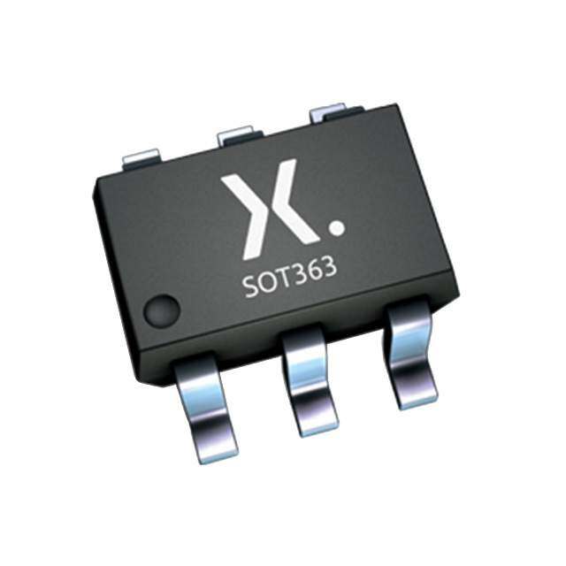
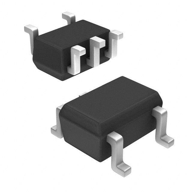
| 供应商器件封装 | 6-TSSOP |
| 元件数 | 2 |
| 其它名称 | 568-10358-2 |
| 包装 | 带卷 (TR) |
| 安装类型 | 表面贴装 |
| 封装/外壳 | 6-TSSOP,SC-88,SOT-363 |
| 工作温度 | -40°C ~ 125°C |
| 标准包装 | 3,000 |
| 每元件位数 | 1 |
| 电压-电源 | 2 V ~ 6 V |
| 电流-输出高,低 | 5.2mA,5.2mA |
| 逻辑类型 | 施密特触发器 - 缓冲器 |


- 商务部:美国ITC正式对集成电路等产品启动337调查
- 曝三星4nm工艺存在良率问题 高通将骁龙8 Gen1或转产台积电
- 太阳诱电将投资9.5亿元在常州建新厂生产MLCC 预计2023年完工
- 英特尔发布欧洲新工厂建设计划 深化IDM 2.0 战略
- 台积电先进制程称霸业界 有大客户加持明年业绩稳了
- 达到5530亿美元!SIA预计今年全球半导体销售额将创下新高
- 英特尔拟将自动驾驶子公司Mobileye上市 估值或超500亿美元
- 三星加码芯片和SET,合并消费电子和移动部门,撤换高东真等 CEO
- 三星电子宣布重大人事变动 还合并消费电子和移动部门
- 海关总署:前11个月进口集成电路产品价值2.52万亿元 增长14.8%


PDF Datasheet 数据手册内容提取
74HC2G17-Q100; 74HCT2G17-Q100 Dual non-inverting Schmitt trigger Rev. 1 — 22 May 2013 Product data sheet 1. General description The 74HC2G17-Q100; 74HCT2G17-Q100 are dual buffers with Schmitt-trigger inputs. Inputs include clamp diodes. This enables the use of current limiting resistors to interface inputs to voltages in excess of V . Schmitt trigger inputs transform slowly changing input CC signals into sharply defined jitter-free output signals. This product has been qualified to the Automotive Electronics Council (AEC) standard Q100 (Grade 1) and is suitable for use in automotive applications. 2. Features and benefits Automotive product qualification in accordance with AEC-Q100 (Grade 1) Specified from 40C to +85C and from 40C to +125C Input levels: For 74HC2G17-Q100: CMOS level For 74HCT2G17-Q100: TTL level Complies with JEDEC standard no. 7A High noise immunity ESD protection: MIL-STD-883, method 3015 exceeds 2000 V HBM JESD22-A114F exceeds 2000V MM JESD22-A115-A exceeds 200V (C = 200 pF, R = 0 ) Low power dissipation Balanced propagation delays Unlimited input rise and fall times Multiple package options 3. Applications Wave and pulse shaper for highly noisy environments Astable multivibrators Monostable multivibrators
74HC2G17-Q100; 74HCT2G17-Q100 Nexperia Dual non-inverting Schmitt trigger 4. Ordering information Table 1. Ordering info rmation Type number Package Temperature range Name Description Version 74HC2G17GW-Q100 40 C to +125 C SC-88 plastic surface-mounted package; 6 leads SOT363 74HC2G17GV-Q100 40 C to +125 C SC-74 plastic surface-mounted package (TSOP6); 6 leads SOT457 74HCT2G17GW-Q100 40 C to +125 C SC-88 plastic surface-mounted package; 6 leads SOT363 74HCT2G17GV-Q100 40 C to +125 C SC-74 plastic surface-mounted package (TSOP6); 6 leads SOT457 5. Marking Table 2. Marking Type number Marking code[1] 74HC2G17GW-Q100 HV 74HC2G17GV-Q100 HV 74HCT2G17GW-Q100 TV 74HCT2G17GV-Q100 TV [1] The pin 1 indicator is located on the lower left corner of the device, below the marking code. 6. Functional diagram 1 6 1 1A 1Y 6 3 2A 2Y 4 3 4 mnb066 mnb067 Fig 1. Logic symbol Fig 2. IEC logic symbol 1A 1Y 2A 2Y mnb068 Fig 3. Logic diagram 74HC_HCT2G17_Q100 All information provided in this document is subject to legal disclaimers. © Nexperia B.V. 2017. All rights reserved Product data sheet Rev. 1 — 22 May 2013 2 of 19
74HC2G17-Q100; 74HCT2G17-Q100 Nexperia Dual non-inverting Schmitt trigger 7. Pinning information 7.1 Pinning (cid:26)(cid:23)(cid:43)(cid:38)(cid:21)(cid:42)(cid:20)(cid:26)(cid:16)(cid:52)(cid:20)(cid:19)(cid:19) (cid:26)(cid:23)(cid:43)(cid:38)(cid:55)(cid:21)(cid:42)(cid:20)(cid:26)(cid:16)(cid:52)(cid:20)(cid:19)(cid:19) (cid:20)(cid:36) (cid:20) (cid:25) (cid:20)(cid:60) (cid:42)(cid:49)(cid:39) (cid:21) (cid:24) (cid:57)(cid:38)(cid:38) (cid:21)(cid:36) (cid:22) (cid:23) (cid:21)(cid:60) (cid:68)(cid:68)(cid:68)(cid:16)(cid:19)(cid:19)(cid:26)(cid:24)(cid:27)(cid:22) Fig 4. Pin configuration 7.2 Pin description Table 3. Pin descripti on Symbol Pin Description 1A 1 data input GND 2 ground (0V) 2A 3 data input 2Y 4 data output V 5 supply voltage CC 1Y 6 data output 8. Functional description Table 4. Function tab le[1] Input Output nA nY L L H H [1] H=HIGH voltage level; L=LOW voltage level. 74HC_HCT2G17_Q100 All information provided in this document is subject to legal disclaimers. © Nexperia B.V. 2017. All rights reserved Product data sheet Rev. 1 — 22 May 2013 3 of 19
74HC2G17-Q100; 74HCT2G17-Q100 Nexperia Dual non-inverting Schmitt trigger 9. Limiting values Table 5. Limiting valu es In accordance with the Absolute Maximum Rating System (IEC 60134). Voltages are referenced to GND (ground = 0 V). Symbol Parameter Conditions Min Max Unit V supply voltage 0.5 +7.0 V CC I input clamping current V < 0.5V or V >V +0.5 V [1] - 20 mA IK I I CC I output clamping current V <0.5V or V >V +0.5V [1] - 20 mA OK O O CC I output current V = 0.5V to V +0.5V [1] - 25 mA O O CC I supply current [1] - 50 mA CC I ground current [1] - 50 mA GND T storage temperature 65 +150 C stg P total power dissipation [2] - 250 mW tot [1] The minimum input and output voltage ratings may be exceeded if the input and output current ratings are observed. [2] For SC-88 and SC-74 packages: above 87.5C the value of Ptotderates linearly with 4.0mW/K. 10. Recommended operating conditions Table 6. Recommend ed operating conditions Symbol Parameter Conditions Min Typ Max Unit 74HC2G17-Q100 V supply voltage 2.0 5.0 6.0 V CC V input voltage 0 - V V I CC V output voltage 0 - V V O CC T ambient temperature 40 +25 +125 C amb 74HCT2G17-Q100 V supply voltage 4.5 5.0 5.5 V CC V input voltage 0 - V V I CC V output voltage 0 - V V O CC T ambient temperature 40 +25 +125 C amb 11. Static characteristics Table 7. Static charac teristics for 74HC2G17 At recommended operating conditions; voltages are referenced to GND (ground=0V). Symbol Parameter Conditions Min Typ Max Unit T = 25 C amb V HIGH-level output voltage V = V or V OH I T+ T I = 20A; V = 2.0V 1.9 2.0 - V O CC I = 20A; V = 4.5V 4.4 4.5 - V O CC I = 20A; V = 6.0V 5.9 6.0 - V O CC I = 4.0mA; V =4.5V 4.18 4.32 - V O CC I =5.2mA; V =6.0V 5.68 5.81 - V O CC 74HC_HCT2G17_Q100 All information provided in this document is subject to legal disclaimers. © Nexperia B.V. 2017. All rights reserved Product data sheet Rev. 1 — 22 May 2013 4 of 19
74HC2G17-Q100; 74HCT2G17-Q100 Nexperia Dual non-inverting Schmitt trigger Table 7. Static characteristics for 74HC2G17 …continued At recommended operating conditions; voltages are referenced to GND (ground=0V). Symbol Parameter Conditions Min Typ Max Unit V LOW-level output voltage V = V or V OL I T+ T I = 20A; V = 2.0V - 0 0.1 V O CC I = 20A; V = 4.5V - 0 0.1 V O CC I = 20A; V = 6.0V - 0 0.1 V O CC I = 4.0mA; V = 4.5V - 0.15 0.26 V O CC I = 5.2mA; V = 6.0V - 0.16 0.26 V O CC I input leakage current V = GND or V ; V = 6.0V - - 0.1 A I I CC CC I supply current V = GND or V ; I = 0 A; - - 1.0 A CC I CC O V = 6.0V CC C input capacitance - 2.0 - pF I T = 40C to +85C amb V HIGH-level output voltage V = V or V OH I T+ T I = 20A; V = 2.0V 1.9 - - V O CC I = 20A; V = 4.5V 4.4 - - V O CC I = 20A; V = 6.0V 5.9 - - V O CC I = 4.0mA; V = 4.5V 4.13 - - V O CC I = 5.2mA; V = 6.0V 5.63 - - V O CC V LOW-level output voltage V = V or V OL I T+ T I = 20A; V = 2.0V - - 0.1 V O CC I = 20A; V = 4.5V - - 0.1 V O CC I = 20A; V = 6.0V - - 0.1 V O CC I = 4.0mA; V = 4.5V - - 0.33 V O CC I = 5.2mA; V = 6.0V - - 0.33 V O CC I input leakage current V = GND or V ; V = 6.0V - - 1.0 A I I CC CC I supply current V = GND or V ; I = 0 A; - - 10.0 A CC I CC O V = 6.0V CC T = 40C to +125C amb V HIGH-level output voltage V = V or V OH I T+ T I = 20A; V = 2.0V 1.9 - - V O CC I = 20A; V = 4.5V 4.4 - - V O CC I = 20A; V = 6.0V 5.9 - - V O CC I = 4.0mA; V = 4.5V 3.7 - - V O CC I = 5.2mA; V = 6.0V 5.2 - - V O CC 74HC_HCT2G17_Q100 All information provided in this document is subject to legal disclaimers. © Nexperia B.V. 2017. All rights reserved Product data sheet Rev. 1 — 22 May 2013 5 of 19
74HC2G17-Q100; 74HCT2G17-Q100 Nexperia Dual non-inverting Schmitt trigger Table 7. Static characteristics for 74HC2G17 …continued At recommended operating conditions; voltages are referenced to GND (ground=0V). Symbol Parameter Conditions Min Typ Max Unit V LOW-level output voltage V = V or V OL I T+ T I = 20A; V = 2.0V - - 0.1 V O CC I = 20A; V = 4.5V - - 0.1 V O CC I = 20A; V = 6.0V - - 0.1 V O CC I = 4.0mA; V = 4.5V - - 0.4 V O CC I = 5.2mA; V = 6.0V - - 0.4 V O CC I input leakage current V = GND or V ; V = 6.0V - - 1.0 A I I CC CC I supply current V = GND or V ; I = 0 A; - - 20.0 A CC I CC O V = 6.0V CC Table 8. Static charac teristics for 74HCT2G17 At recommended operating conditions; voltages are referenced to GND (ground=0V). Symbol Parameter Conditions Min Typ Max Unit T = 25 C amb V HIGH-level output voltage V = V or V ; V = 4.5V OH I T+ T CC I = 20A 4.4 4.5 - V O I = 4.0mA 4.18 4.32 - V O V LOW-level output voltage V = V or V ; V = 4.5V OL I T+ T CC I = 20A - 0 0.1 V O I = 4.0mA - 0.15 0.26 V O I input leakage current V = GND or V ; V = 5.5V - - 0.1 A I I CC CC I supply current V = GND or V ; I = 0A; - - 1.0 A CC I CC O V = 5.5V CC I additional supply current V = V 2.1V; - - 300 A CC I CC V =4.5Vto 5.5V; I = 0 A CC O C input capacitance - 2.0 - pF I T = 40C to +85C amb V HIGH-level output voltage V = V or V ; V = 4.5V OH I T+ T CC I = 20A 4.4 - - V O I = 4.0mA 4.13 - - V O V LOW-level output voltage V = V or V ; V = 4.5V OL I T+ T CC I = 20A - - 0.1 V O I = 4.0mA - - 0.33 V O I input leakage current V = GND or V ; V = 5.5V - - 1.0 A I I CC CC I supply current V = GND or V ; I = 0A; - - 10.0 A CC I CC O V = 5.5V CC I additional supply current V = V 2.1V; - - 375 A CC I CC V =4.5Vto 5.5V; I = 0 A CC O 74HC_HCT2G17_Q100 All information provided in this document is subject to legal disclaimers. © Nexperia B.V. 2017. All rights reserved Product data sheet Rev. 1 — 22 May 2013 6 of 19
74HC2G17-Q100; 74HCT2G17-Q100 Nexperia Dual non-inverting Schmitt trigger Table 8. Static characteristics for 74HCT2G17 …continued At recommended operating conditions; voltages are referenced to GND (ground=0V). Symbol Parameter Conditions Min Typ Max Unit T = 40C to +125C amb V HIGH-level output voltage V = V or V ; V = 4.5V OH I T+ T CC I = 20A 4.4 - - V O I = 4.0mA 3.7 - - V O V LOW-level output voltage V = V or V ; V = 4.5V OL I T+ T CC I = 20A - - 0.1 V O I = 4.0mA - - 0.4 V O I input leakage current V = GND or V ; V = 5.5V - - 1.0 A I I CC CC I supply current V = GND or V ; I = 0A; - - 20.0 A CC I CC O V = 5.5V CC I additional supply current V = V 2.1V; - - 410 A CC I CC V =4.5Vto 5.5V; I = 0 A CC O 12. Dynamic characteristics Table 9. Dynamic cha racteristics Voltages are referenced to GND (ground=0V); for test circuit see Figure6. Symbol Parameter Conditions 25 C 40C to+125 C Unit Min Typ Max Min Max Max (85C) (125C) 74HC2G17-Q100 t propagation delay nA to nY; see Figure5 [1] pd V =2.0 V; C =50pF - 36 115 - 140 175 ns CC L V =4.5 V; C =50pF - 12 22 - 27 34 ns CC L V =6.0V; C =50pF - 10 18 - 22 28 ns CC L t transition time nY; see Figure5 [2] t V = 2.0V; C =50pF - 20 75 - 95 110 ns CC L V = 4.5V; C =50pF - 7 15 - 19 22 ns CC L V = 6.0V; C =50pF - 5 13 - 16 19 ns CC L C power dissipation V = GND to V [3] - 10 - - - - pF PD I CC capacitance 74HC_HCT2G17_Q100 All information provided in this document is subject to legal disclaimers. © Nexperia B.V. 2017. All rights reserved Product data sheet Rev. 1 — 22 May 2013 7 of 19
74HC2G17-Q100; 74HCT2G17-Q100 Nexperia Dual non-inverting Schmitt trigger Table 9. Dynamic characteristics …continued Voltages are referenced to GND (ground=0V); for test circuit see Figure6. Symbol Parameter Conditions 25 C 40C to+125 C Unit Min Typ Max Min Max Max (85C) (125C) 74HCT2G17-Q100 t propagation delay nA to nY; see Figure5 [1] pd V = 4.5V; C =50pF - 21 29 - 36 45 ns CC L t transition time nY; see Figure5 [2] t V =4.5V; C =50 pF - 6 15 - 19 22 ns CC L C power dissipation V = GND to V 1.5 V [3] - 10 - - - - pF PD I CC capacitance [1] t is the same as t and t pd PLH PHL [2] t is the same as t and t t TLH THL [3] CPD is used to determine the dynamic power dissipation (PD in W). PD=CPDVCC2fiN+(CLVCC2fo) where: f =input frequency in MHz; i f =output frequency in MHz; o C =output load capacitance in pF; L V =supply voltage in V; CC N=number of inputs switching; (CLVCC2fo)=sum of the outputs. 13. Waveforms VI nA input VM VM GND tPLH tPHL VOH 90 % 90 % nY output 10 % 10 % VOL tTLH tTHL 001aaf302 Measurement points are given in Table10. VOL and VOH are typical voltage output levels that occur with the output load. Fig 5. The data input (nA) to output (nY) propagation delays and output transition times Table 10. Measuremen t points Type Input Output V V t = t V M I r f M 74HC2G17-Q100 0.5V GND to V 6.0 ns 0.5V CC CC CC 74HCT2G17-Q100 1.3V GND to 3.0 V 6.0 ns 1.3V 74HC_HCT2G17_Q100 All information provided in this document is subject to legal disclaimers. © Nexperia B.V. 2017. All rights reserved Product data sheet Rev. 1 — 22 May 2013 8 of 19
74HC2G17-Q100; 74HCT2G17-Q100 Nexperia Dual non-inverting Schmitt trigger V V CC CC PULSE VI VO RL = 1 kΩ D.U.T open GENERATOR RT CL 50 pF mgk563 Test data is given in Table11. Definitions test circuit: RL = Load resistance. CL = Load capacitance including jig and probe capacitance. R = Termination resistance should be equal to output impedance Z of the pulse generator. T o Fig 6. Test circuit for measuring switching times Table 11. Test data Type Input Test V t, t t , t I r f PHL PLH 74HC2G17-Q100 GND to V 6ns open CC 74HCT2G17-Q100 GND to 3.0 V 6ns open 14. Transfer characteristics Table 12. Transfer cha racteristics Voltages are referenced to GND (ground=0V); for test circuit see Figure6. Symbol Parameter Conditions 25 C 40C to+125 C Unit Min Typ Max Min Max Max (85C) (125C) 74HC2G17-Q100 V positive-going see Figure7, Figure8 T+ threshold voltage V = 2.0 V 1.00 1.18 1.50 1.00 1.50 1.50 V CC V = 4.5 V 2.30 2.60 3.15 2.30 3.15 3.15 V CC V = 6.0 V 3.00 3.46 4.20 3.00 4.20 4.20 V CC V negative-going see Figure7, Figure8 T threshold voltage V = 2.0 V 0.30 0.60 0.90 0.30 0.90 0.90 V CC V = 4.5 V 1.13 1.47 2.00 1.13 2.00 2.00 V CC V = 6.0 V 1.50 2.06 2.60 1.50 2.60 2.60 V CC V hysteresis voltage V V ; see Figure7, H T+ T Figure8 and Figure9 V = 2.0 V 0.30 0.60 1.00 0.30 1.00 1.00 V CC V = 4.5 V 0.60 1.13 1.40 0.60 1.40 1.40 V CC V = 6.0 V 0.80 1.40 1.70 0.80 1.70 1.70 V CC 74HC_HCT2G17_Q100 All information provided in this document is subject to legal disclaimers. © Nexperia B.V. 2017. All rights reserved Product data sheet Rev. 1 — 22 May 2013 9 of 19
74HC2G17-Q100; 74HCT2G17-Q100 Nexperia Dual non-inverting Schmitt trigger Table 12. Transfer characteristics …continued Voltages are referenced to GND (ground=0V); for test circuit see Figure6. Symbol Parameter Conditions 25 C 40C to+125 C Unit Min Typ Max Min Max Max (85C) (125C) 74HCT2G17-Q100 V positive-going see Figure7 and Figure8 T+ threshold voltage V = 4.5 V 1.20 1.58 1.90 1.20 1.90 1.90 V CC V = 5.5 V 1.40 1.78 2.10 1.40 2.10 2.10 V CC V negative-going see Figure7 and Figure8 T threshold voltage V = 4.5 V 0.50 0.87 1.20 0.50 1.20 1.20 V CC V = 5.5 V 0.60 1.11 1.40 0.60 1.40 1.40 V CC V hysteresis voltage V V ; see Figure7, H T+ T Figure8 and Figure10 V = 4.5 V 0.40 0.71 - 0.40 - - V CC V = 5.5 V 0.40 0.67 - 0.40 - - V CC 15. Waveforms transfer characteristics VO VT+ VI VH VT− VO VH VI mnb155 VT− VT+ mnb154 V and V limits at 70% and 20%. T+ T Fig 7. Transfer characteristic Fig 8. Definition of V , V and V T+ T H 74HC_HCT2G17_Q100 All information provided in this document is subject to legal disclaimers. © Nexperia B.V. 2017. All rights reserved Product data sheet Rev. 1 — 22 May 2013 10 of 19
74HC2G17-Q100; 74HCT2G17-Q100 Nexperia Dual non-inverting Schmitt trigger mna028 mna029 100 1.0 ICC (mA) ICC (μA) 0.8 0.6 50 0.4 0.2 0 0 0 1.0 VI (V) 2.0 0 2.5 VI (V) 5.0 a. V = 2.0V b. V = 4.5V CC CC mna030 1.6 ICC (mA) 0.8 0 0 3.0 6.0 VI (V) c. V = 6.0V CC Fig 9. Typical 74HC2G17 transfer characteristics 74HC_HCT2G17_Q100 All information provided in this document is subject to legal disclaimers. © Nexperia B.V. 2017. All rights reserved Product data sheet Rev. 1 — 22 May 2013 11 of 19
74HC2G17-Q100; 74HCT2G17-Q100 Nexperia Dual non-inverting Schmitt trigger mna031 mna032 2.0 3.0 ICC (ImCAC) (mA) 2.0 1.0 1.0 0 0 0 2.5 5.0 0 3.0 6.0 VI (V) VI (V) a. V = 4.5V. b. V = 5.5V. CC CC Fig 10. Typical 74HCT2G17-Q100 transfer characteristics 16. Application information The slow input rise and fall times cause additional power dissipation which can be calculated using the following formula: P =f (t I +t I )V where: add i r CC(AV) f CC(AV) CC P =additional power dissipation (W); add f =input frequency (MHz); i t =input rise time (ns); 10%to90%; r t =input fall time (ns); 90%to10%; f I =average additional supply current (A). CC(AV) I differs with positive or negative input transitions, as shown inFigure11 and CC(AV) Figure12. 74HC_HCT2G17_Q100 All information provided in this document is subject to legal disclaimers. © Nexperia B.V. 2017. All rights reserved Product data sheet Rev. 1 — 22 May 2013 12 of 19
74HC2G17-Q100; 74HCT2G17-Q100 Nexperia Dual non-inverting Schmitt trigger mna036 200 ΔICC(AV) (μA) 150 positive-going edge 100 50 negative-going edge 0 0 2.0 4.0 6.0 VCC (V) Fig 11. I as a function of V for 74HC2G17-Q100; linear change of V between 0.1V to 0.9V CC(AV) CC I CC CC mna058 200 ΔICC(AV) (μA) 150 positive-going edge 100 negative-going 50 edge 0 0 2 4 VCC (V) 6 Fig 12. I as a function of V for 74HCT2G17-Q100; linear change of V between 0.1V to 0.9V CC(AV) CC I CC CC 74HC_HCT2G17_Q100 All information provided in this document is subject to legal disclaimers. © Nexperia B.V. 2017. All rights reserved Product data sheet Rev. 1 — 22 May 2013 13 of 19
74HC2G17-Q100; 74HCT2G17-Q100 Nexperia Dual non-inverting Schmitt trigger 17. Package outline Plastic surface-mounted package; 6 leads SOT363 D B E A X y HE v M A 6 5 4 Q pin 1 index A A1 1 2 3 c e1 bp w M B Lp e detail X 0 1 2 mm scale DIMENSIONS (mm are the original dimensions) A1 UNIT A max bp c D E e e1 HE Lp Q v w y 1.1 0.30 0.25 2.2 1.35 2.2 0.45 0.25 mm 0.1 1.3 0.65 0.2 0.2 0.1 0.8 0.20 0.10 1.8 1.15 2.0 0.15 0.15 OUTLINE REFERENCES EUROPEAN ISSUE DATE VERSION IEC JEDEC JEITA PROJECTION 04-11-08 SOT363 SC-88 06-03-16 Fig 13. Package outline SOT363 (SC-88) 74HC_HCT2G17_Q100 All information provided in this document is subject to legal disclaimers. © Nexperia B.V. 2017. All rights reserved Product data sheet Rev. 1 — 22 May 2013 14 of 19
74HC2G17-Q100; 74HCT2G17-Q100 Nexperia Dual non-inverting Schmitt trigger Plastic surface-mounted package (TSOP6); 6 leads SOT457 D B E A X y HE v M A 6 5 4 Q pin 1 index A A1 c 1 2 3 Lp e bp w M B detail X 0 1 2 mm scale DIMENSIONS (mm are the original dimensions) UNIT A A1 bp c D E e HE Lp Q v w y 1.1 0.1 0.40 0.26 3.1 1.7 3.0 0.6 0.33 mm 0.95 0.2 0.2 0.1 0.9 0.013 0.25 0.10 2.7 1.3 2.5 0.2 0.23 OUTLINE REFERENCES EUROPEAN ISSUE DATE VERSION IEC JEDEC JEITA PROJECTION 05-11-07 SOT457 SC-74 06-03-16 Fig 14. Package outline SOT457 (SC-74) 74HC_HCT2G17_Q100 All information provided in this document is subject to legal disclaimers. © Nexperia B.V. 2017. All rights reserved Product data sheet Rev. 1 — 22 May 2013 15 of 19
74HC2G17-Q100; 74HCT2G17-Q100 Nexperia Dual non-inverting Schmitt trigger 18. Abbreviations Table 13. Abbreviation s Acronym Description CMOS Complementary Metal Oxide Semiconductor TTL Transistor-Transistor Logic HBM Human Body Model ESD ElectroStatic Discharge MM Machine Model DUT Device Under Test MIL Military 19. Revision history T able 14. Revision history Document ID Release date Data sheet status Change notice Supersedes 74HC_HCT2G17_Q100 v.1 20130522 Product data sheet - - 74HC_HCT2G17_Q100 All information provided in this document is subject to legal disclaimers. © Nexperia B.V. 2017. All rights reserved Product data sheet Rev. 1 — 22 May 2013 16 of 19
74HC2G17-Q100; 74HCT2G17-Q100 Nexperia Dual non-inverting Schmitt trigger 20. Legal information 20.1 Data sheet status Document status[1][2] Product status[3] Definition Objective [short] data sheet Development This document contains data from the objective specification for product development. Preliminary [short] data sheet Qualification This document contains data from the preliminary specification. Product [short] data sheet Production This document contains the product specification. [1] Please consult the most recently issued document before initiating or completing a design. [2] The term ‘short data sheet’ is explained in section “Definitions”. [3] The product status of device(s) described in this document may have changed since this document was published and may differ in case of multiple devices. The latest product status information is available on the Internet at URLhttp://www.nexperia.com. 20.2 Definitions Suitability for use in automotive applications — This Nexperia product has been qualified for use in automotive applications. Unless otherwise agreed in writing, the product is not designed, Draft — The document is a draft version only. The content is still under authorized or warranted to be suitable for use in life support, life-critical or internal review and subject to formal approval, which may result in safety-critical systems or equipment, nor in applications where failure or modifications or additions. Nexperia does not give any malfunction of a Nexperia product can reasonably be expected representations or warranties as to the accuracy or completeness of to result in personal injury, death or severe property or environmental information included herein and shall have no liability for the consequences of damage. Nexperia and its suppliers accept no liability for use of such information. inclusion and/or use of Nexperia products in such equipment or Short data sheet — A short data sheet is an extract from a full data sheet applications and therefore such inclusion and/or use is at the customer's own with the same product type number(s) and title. A short data sheet is intended risk. for quick reference only and should not be relied upon to contain detailed and Applications — Applications that are described herein for any of these full information. For detailed and full information see the relevant full data products are for illustrative purposes only. Nexperia makes no sheet, which is available on request via the local Nexperia sales representation or warranty that such applications will be suitable for the office. In case of any inconsistency or conflict with the short data sheet, the specified use without further testing or modification. full data sheet shall prevail. Customers are responsible for the design and operation of their applications Product specification — The information and data provided in a Product and products using Nexperia products, and Nexperia data sheet shall define the specification of the product as agreed between accepts no liability for any assistance with applications or customer product Nexperia and its customer, unless Nexperia and design. It is customer’s sole responsibility to determine whether the Nexperia customer have explicitly agreed otherwise in writing. In no event however, product is suitable and fit for the customer’s applications and shall an agreement be valid in which the Nexperia product is products planned, as well as for the planned application and use of deemed to offer functions and qualities beyond those described in the customer’s third party customer(s). Customers should provide appropriate Product data sheet. design and operating safeguards to minimize the risks associated with their applications and products. 20.3 Disclaimers Nexperia does not accept any liability related to any default, damage, costs or problem which is based on any weakness or default in the customer’s applications or products, or the application or use by customer’s Limited warranty and liability — Information in this document is believed to third party customer(s). Customer is responsible for doing all necessary be accurate and reliable. However, Nexperia does not give any testing for the customer’s applications and products using Nexperia representations or warranties, expressed or implied, as to the accuracy or products in order to avoid a default of the applications and completeness of such information and shall have no liability for the the products or of the application or use by customer’s third party consequences of use of such information. Nexperia takes no customer(s). Nexperia does not accept any liability in this respect. responsibility for the content in this document if provided by an information source outside of Nexperia. Limiting values — Stress above one or more limiting values (as defined in the Absolute Maximum Ratings System of IEC60134) will cause permanent In no event shall Nexperia be liable for any indirect, incidental, damage to the device. Limiting values are stress ratings only and (proper) punitive, special or consequential damages (including - without limitation - lost operation of the device at these or any other conditions above those given in profits, lost savings, business interruption, costs related to the removal or the Recommended operating conditions section (if present) or the replacement of any products or rework charges) whether or not such Characteristics sections of this document is not warranted. Constant or damages are based on tort (including negligence), warranty, breach of repeated exposure to limiting values will permanently and irreversibly affect contract or any other legal theory. the quality and reliability of the device. Notwithstanding any damages that customer might incur for any reason Terms and conditions of commercial sale — Nexperia whatsoever, Nexperia’s aggregate and cumulative liability towards products are sold subject to the general terms and conditions of commercial customer for the products described herein shall be limited in accordance with the Terms and conditions of commercial sale of Nexperia. sale, as published at http://www.nexperia.com/profile/terms, unless otherwise agreed in a valid written individual agreement. In case an individual Right to make changes — Nexperia reserves the right to make agreement is concluded only the terms and conditions of the respective changes to information published in this document, including without agreement shall apply. Nexperia hereby expressly objects to limitation specifications and product descriptions, at any time and without applying the customer’s general terms and conditions with regard to the notice. This document supersedes and replaces all information supplied prior purchase of Nexperia products by customer. to the publication hereof. 74HC_HCT2G17_Q100 All information provided in this document is subject to legal disclaimers. © Nexperia B.V. 2017. All rights reserved Product data sheet Rev. 1 — 22 May 2013 17 of 19
74HC2G17-Q100; 74HCT2G17-Q100 Nexperia Dual non-inverting Schmitt trigger No offer to sell or license — Nothing in this document may be interpreted or Translations — A non-English (translated) version of a document is for construed as an offer to sell products that is open for acceptance or the grant, reference only. The English version shall prevail in case of any discrepancy conveyance or implication of any license under any copyrights, patents or between the translated and English versions. other industrial or intellectual property rights. Export control — This document as well as the item(s) described herein 20.4 Trademarks may be subject to export control regulations. Export might require a prior authorization from competent authorities. Notice: All referenced brands, product names, service names and trademarks are the property of their respective owners. 21. Contact information For more information, please visit: http://www.nexperia.com For sales office addresses, please send an email to: salesaddresses@nexperia.com 74HC_HCT2G17_Q100 All information provided in this document is subject to legal disclaimers. © Nexperia B.V. 2017. All rights reserved Product data sheet Rev. 1 — 22 May 2013 18 of 19
74HC2G17-Q100; 74HCT2G17-Q100 Nexperia Dual non-inverting Schmitt trigger 22. Contents 1 General description. . . . . . . . . . . . . . . . . . . . . . 1 2 Features and benefits . . . . . . . . . . . . . . . . . . . . 1 3 Applications. . . . . . . . . . . . . . . . . . . . . . . . . . . . 1 4 Ordering information. . . . . . . . . . . . . . . . . . . . . 2 5 Marking. . . . . . . . . . . . . . . . . . . . . . . . . . . . . . . . 2 6 Functional diagram . . . . . . . . . . . . . . . . . . . . . . 2 7 Pinning information. . . . . . . . . . . . . . . . . . . . . . 3 7.1 Pinning . . . . . . . . . . . . . . . . . . . . . . . . . . . . . . . 3 7.2 Pin description . . . . . . . . . . . . . . . . . . . . . . . . . 3 8 Functional description . . . . . . . . . . . . . . . . . . . 3 9 Limiting values. . . . . . . . . . . . . . . . . . . . . . . . . . 4 10 Recommended operating conditions. . . . . . . . 4 11 Static characteristics. . . . . . . . . . . . . . . . . . . . . 4 12 Dynamic characteristics. . . . . . . . . . . . . . . . . . 7 13 Waveforms . . . . . . . . . . . . . . . . . . . . . . . . . . . . . 8 14 Transfer characteristics . . . . . . . . . . . . . . . . . . 9 15 Waveforms transfer characteristics. . . . . . . . 10 16 Application information. . . . . . . . . . . . . . . . . . 12 17 Package outline. . . . . . . . . . . . . . . . . . . . . . . . 14 18 Abbreviations. . . . . . . . . . . . . . . . . . . . . . . . . . 16 19 Revision history. . . . . . . . . . . . . . . . . . . . . . . . 16 20 Legal information. . . . . . . . . . . . . . . . . . . . . . . 17 20.1 Data sheet status . . . . . . . . . . . . . . . . . . . . . . 17 20.2 Definitions. . . . . . . . . . . . . . . . . . . . . . . . . . . . 17 20.3 Disclaimers. . . . . . . . . . . . . . . . . . . . . . . . . . . 17 20.4 Trademarks. . . . . . . . . . . . . . . . . . . . . . . . . . . 18 21 Contact information. . . . . . . . . . . . . . . . . . . . . 18 22 Contents. . . . . . . . . . . . . . . . . . . . . . . . . . . . . . 19 © Nexperia B.V. 2017. All rights reserved For more information, please visit: http://www.nexperia.com For sales office addresses, please send an email to: salesaddresses@nexperia.com Date of release: 22 May 2013