ICGOO在线商城 > 集成电路(IC) > 逻辑 - 缓冲器,驱动器,接收器,收发器 > SN74LS244DWR

 Datasheet下载
- 型号: SN74LS244DWR
- 制造商: Texas Instruments
- 库位|库存: xxxx|xxxx
- 要求:
| 数量阶梯 | 香港交货 | 国内含税 |
| +xxxx | $xxxx | ¥xxxx |
查看当月历史价格
查看今年历史价格
SN74LS244DWR产品简介:
ICGOO电子元器件商城为您提供SN74LS244DWR由Texas Instruments设计生产,在icgoo商城现货销售,并且可以通过原厂、代理商等渠道进行代购。 SN74LS244DWR价格参考¥4.68-¥5.85。Texas InstrumentsSN74LS244DWR封装/规格:逻辑 - 缓冲器,驱动器,接收器,收发器, Buffer, Non-Inverting 2 Element 4 Bit per Element 3-State Output 20-SOIC。您可以下载SN74LS244DWR参考资料、Datasheet数据手册功能说明书,资料中有SN74LS244DWR 详细功能的应用电路图电压和使用方法及教程。
SN74LS244DWR是德州仪器(Texas Instruments)生产的一款八位缓冲器/驱动器,属于逻辑集成电路中的缓冲器、驱动器类别。该器件内部包含两个独立的四路非反相缓冲器,具有高驱动输出能力,适用于需要信号放大和隔离的数字系统。

主要应用场景包括:

1. 总线驱动:在微处理器或微控制器系统中,用于驱动地址总线或数据总线,增强信号传输能力,确保信号在长距离或多负载条件下仍能稳定传输。

2. 存储器接口:作为存储器与控制单元之间的缓冲,防止负载过重导致信号失真,提升系统稳定性。

3. 数字系统信号隔离:在复杂的数字电路中,用于隔离前后级电路,减少相互干扰,提高抗噪能力。

4. 工业控制设备:广泛应用于PLC(可编程逻辑控制器)、工控机等工业自动化设备中,用于电平转换和信号整形。

5. 通信系统:在低速通信接口中作为线路驱动器,增强信号驱动能力,保障数据可靠传输。

SN74LS244DWR采用SOIC-20封装,适合表面贴装工艺,工作温度范围为商业级(0°C 至 70°C),适用于对成本和功耗有一定要求的中低端数字系统。由于其基于LS(低功耗肖特基)工艺,具备较快的开关速度和较低的功耗,是传统TTL逻辑设计中的常用器件。
| 参数 | 数值 |
| 产品目录 | 集成电路 (IC)半导体 |
| 描述 | IC BUFF/DVR TRI-ST DUAL 20SOIC缓冲器和线路驱动器 Tri-State Octal |
| 产品分类 | |
| 品牌 | Texas Instruments |
| 产品手册 | |
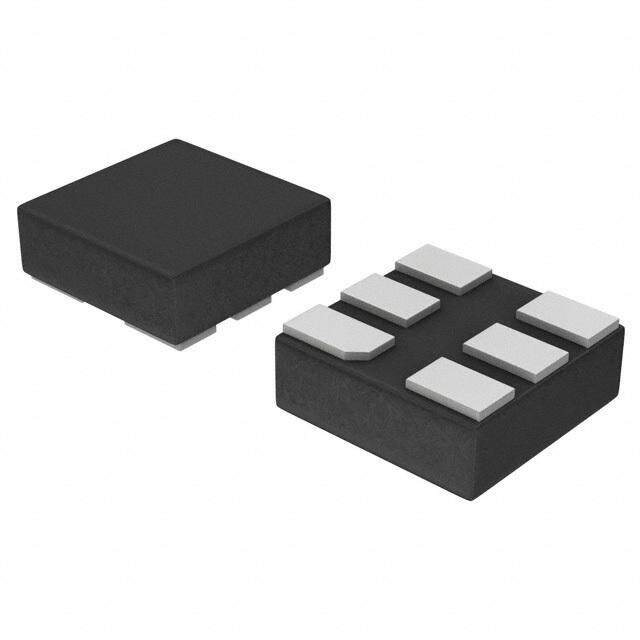
| 产品图片 |
|
| rohs | 符合RoHS无铅 / 符合限制有害物质指令(RoHS)规范要求 |
| 产品系列 | 逻辑集成电路,缓冲器和线路驱动器,Texas Instruments SN74LS244DWR74LS |
| 数据手册 | |
| 产品型号 | SN74LS244DWR |
| 产品目录页面 | |
| 产品种类 | 缓冲器和线路驱动器 |
| 传播延迟时间 | 18 ns at 5 V |
| 低电平输出电流 | 24 mA |
| 供应商器件封装 | 20-SOIC |
| 元件数 | 2 |
| 其它名称 | 296-1213-1 |
| 包装 | 剪切带 (CT) |
| 单位重量 | 500.700 mg |
| 商标 | Texas Instruments |
| 安装类型 | 表面贴装 |
| 安装风格 | SMD/SMT |
| 封装 | Reel |
| 封装/外壳 | 20-SOIC(0.295",7.50mm 宽) |
| 封装/箱体 | SOIC-20 |
| 工作温度 | 0°C ~ 70°C |
| 工厂包装数量 | 2000 |
| 最大工作温度 | + 70 C |
| 最小工作温度 | 0 C |
| 极性 | Non-Inverting |
| 标准包装 | 1 |
| 每元件位数 | 4 |
| 每芯片的通道数量 | 8 |
| 电压-电源 | 4.75 V ~ 5.25 V |
| 电流-输出高,低 | 15mA,24mA |
| 电源电压-最大 | 5.25 V |
| 电源电压-最小 | 4.75 V |
| 电源电流 | 0.046 mA |
| 系列 | SN74LS244 |
| 输入线路数量 | 8 |
| 输出类型 | 3-State |
| 输出线路数量 | 8 |
| 逻辑类型 | 缓冲器/线路驱动器,非反相 |
| 逻辑系列 | LS |
| 高电平输出电流 | - 15 mA |


- 商务部:美国ITC正式对集成电路等产品启动337调查
- 曝三星4nm工艺存在良率问题 高通将骁龙8 Gen1或转产台积电
- 太阳诱电将投资9.5亿元在常州建新厂生产MLCC 预计2023年完工
- 英特尔发布欧洲新工厂建设计划 深化IDM 2.0 战略
- 台积电先进制程称霸业界 有大客户加持明年业绩稳了
- 达到5530亿美元!SIA预计今年全球半导体销售额将创下新高
- 英特尔拟将自动驾驶子公司Mobileye上市 估值或超500亿美元
- 三星加码芯片和SET,合并消费电子和移动部门,撤换高东真等 CEO
- 三星电子宣布重大人事变动 还合并消费电子和移动部门
- 海关总署:前11个月进口集成电路产品价值2.52万亿元 增长14.8%


PDF Datasheet 数据手册内容提取
Product Sample & Technical Tools & Support & Folder Buy Documents Software Community SN54LS240,SN54LS241,SN54LS244,SN54S240,SN54S241,SN54S244 SN74LS240,SN74LS241,SN74LS244,SN74S240,SN74S241,SN74S244 SDLS144D–APRIL1985–REVISEDOCTOBER2016 SNx4LS24x, SNx4S24x Octal Buffers and Line Drivers With 3-State Outputs 1 Features 3 Description • InputsTolerantDownto2V,CompatibleWith The SNx4LS24x, SNx4S24x octal buffers and line 1 drivers are designed specifically to improve both the 3.3-Vor2.5-VLogicInputs performance and density of three-state memory • Maximumt of15nsat5V pd address drivers, clock drivers, and bus-oriented • 3-StateOutputsDriveBusLinesorBufferMemory receiversandtransmitters.Thedesignerhasachoice AddressRegisters of selected combinations of inverting and non- inverting outputs, symmetrical, active-low output- • PNPInputsReduceDCLoading control (G) inputs, and complementary output-control • HysteresisatInputsImprovesNoiseMargins (G and G) inputs. These devices feature high fan-out, improved fan-in, and 400-mV noise margin. The 2 Applications SN74LS24x and SN74S24x devices can be used to • Servers driveterminatedlinesdownto133Ω. • LEDDisplays DeviceInformation(1) • NetworkSwitches PARTNUMBER PACKAGE BODYSIZE(NOM) • TelecomInfrastructure CDIP(20)–J 24.20mm×6.92mm • MotorDrivers SN54LS24x, CFP(20)–W 7.02mm×13.72mm SN54S24x • I/OExpanders LCCC(20)–FK 8.89mm×8.89mm SN74LS240, SSOP(20)–DB 7.20mm×5.30mm SN74LS244 SN74LS24x, SOIC(20)–DW 12.80mm×7.50mm SN74S24x PDIP(20)–N 24.33mm×6.35mm SN74LS24x SOP(20)–NS 7.80mm×12.60mm (1) For all available packages, see the orderable addendum at theendofthedatasheet. LogicDiagram(PositiveLogic) (cid:181)/6240, (cid:181)6240 1 An IMPORTANT NOTICE at the end of this data sheet addresses availability, warranty, changes, use in safety-critical applications, intellectualpropertymattersandotherimportantdisclaimers.PRODUCTIONDATA. On products compliant to MIL-PRF-38535, all parameters are testedunlessotherwisenoted.Onallotherproducts,production processingdoesnotnecessarilyincludetestingofallparameters.
SN54LS240,SN54LS241,SN54LS244,SN54S240,SN54S241,SN54S244 SN74LS240,SN74LS241,SN74LS244,SN74S240,SN74S241,SN74S244 SDLS144D–APRIL1985–REVISEDOCTOBER2016 www.ti.com Table of Contents 1 Features.................................................................. 1 8.2 FunctionalBlockDiagrams.....................................11 2 Applications........................................................... 1 8.3 FeatureDescription.................................................12 3 Description............................................................. 1 8.4 DeviceFunctionalModes........................................12 4 RevisionHistory..................................................... 2 9 ApplicationandImplementation........................ 14 9.1 ApplicationInformation............................................14 5 PinConfigurationandFunctions......................... 3 9.2 TypicalApplication..................................................14 6 Specifications......................................................... 4 9.3 SystemExamples...................................................15 6.1 AbsoluteMaximumRatings......................................4 10 PowerSupplyRecommendations..................... 17 6.2 ESDRatings..............................................................4 11 Layout................................................................... 17 6.3 RecommendedOperatingConditions.......................4 6.4 ThermalInformation .................................................5 11.1 LayoutGuidelines.................................................17 6.5 ElectricalCharacteristics–SNx4LS24x....................5 11.2 LayoutExample....................................................17 6.6 ElectricalCharacteristics–SNx4S24x......................5 12 DeviceandDocumentationSupport................. 18 6.7 SwitchingCharacteristics–SNx4LS24x...................6 12.1 RelatedLinks........................................................18 6.8 SwitchingCharacteristics–SNx4S24x.....................6 12.2 ReceivingNotificationofDocumentationUpdates18 6.9 TypicalCharacteristics..............................................7 12.3 CommunityResource............................................18 7 ParameterMeasurementInformation..................7 12.4 Trademarks...........................................................18 7.1 SN54LS24xandSN74LS24xDevices......................7 12.5 ElectrostaticDischargeCaution............................18 7.2 SN54S24xandSN74S24xDevices..........................9 12.6 Glossary................................................................18 8 DetailedDescription............................................ 11 13 Mechanical,Packaging,andOrderable Information........................................................... 19 8.1 Overview.................................................................11 4 Revision History NOTE:Pagenumbersforpreviousrevisionsmaydifferfrompagenumbersinthecurrentversion. ChangesfromRevisionC(May2010)toRevisionD Page • AddedApplicationssection,ESDRatingstable,FeatureDescriptionsection,DeviceFunctionalModes,Application andImplementationsection,PowerSupplyRecommendationssection,Layoutsection,DeviceandDocumentation Supportsection,andMechanical,Packaging,andOrderableInformationsection................................................................ 1 • DeletedOrderingInformationtable;seePOAattheendofthedatasheet........................................................................... 1 • ChangedRθ valuesintheThermalInformationtablefrom70to94.3(DB),from58to90.3(DW),from69to50.6 JA (N),andfrom60to76.6(NS)................................................................................................................................................. 5 2 SubmitDocumentationFeedback Copyright©1985–2016,TexasInstrumentsIncorporated ProductFolderLinks:SN54LS240 SN54LS241 SN54LS244 SN54S240 SN54S241 SN54S244SN74LS240 SN74LS241 SN74LS244 SN74S240 SN74S241 SN74S244
SN54LS240,SN54LS241,SN54LS244,SN54S240,SN54S241,SN54S244 SN74LS240,SN74LS241,SN74LS244,SN74S240,SN74S241,SN74S244 www.ti.com SDLS144D–APRIL1985–REVISEDOCTOBER2016 5 Pin Configuration and Functions DB,DW,J,N,NS,orWPackage FKPackage 20-PinSSOP,SOIC,CDIP,PDIP,SOP,orCFP 20-PinLCCC TopView TopView 11AG1 12 2109 V2GCC/ 2G 2Y4 1A1 1G VCC 2G/2G 2Y4 3 18 1Y1 1A2 4 17 2A4 3 2 1 0 9 2 1 2Y3 5 16 1Y2 1A2 4 18 1Y1 1A3 6 15 2A3 2Y2 7 14 1Y3 2Y3 5 17 2A4 1A4 8 13 2A2 1A3 6 16 1Y2 2Y1 9 12 1Y4 2Y2 7 15 2A3 GND 10 11 2A1 1A4 8 14 1Y3 Not to scale 9 10 11 12 13 Not to scale 1 D 1 4 2 Y N A Y A 2 G 2 1 2 PinFunctions PIN I/O DESCRIPTION NO. NAME 1 1G I Channel1outputenable 2 1A1 I Channel1,Aside1 3 2Y4 O Channel2,Yside4 4 1A2 I Channel1,Aside2 5 2Y3 O Channel2,Yside3 6 1A3 I Channel1,Aside3 7 2Y2 O Channel2,Yside2 8 1A4 I Channel1,Aside4 9 2Y1 O Channel2,Yside1 10 GND — Ground 11 2A1 I Channel2,Aside1 12 1Y4 O Channel1,Yside4 13 2A2 I Channel2,Aside2 14 1Y3 O Channel1,Yside3 15 2A3 I Channel2,Aside3 16 1Y2 O Channel1,Yside2 17 2A4 I Channel2,Aside4 18 1Y1 O Channel1,Yside1 19 2G/2G(1) I Channel2outputenable 20 V — Powersupply CC (1) 2GforSNx4LS241andSNx4S241or2Gforallotherdrivers. Copyright©1985–2016,TexasInstrumentsIncorporated SubmitDocumentationFeedback 3 ProductFolderLinks:SN54LS240 SN54LS241 SN54LS244 SN54S240 SN54S241 SN54S244SN74LS240 SN74LS241 SN74LS244 SN74S240 SN74S241 SN74S244
SN54LS240,SN54LS241,SN54LS244,SN54S240,SN54S241,SN54S244 SN74LS240,SN74LS241,SN74LS244,SN74S240,SN74S241,SN74S244 SDLS144D–APRIL1985–REVISEDOCTOBER2016 www.ti.com 6 Specifications 6.1 Absolute Maximum Ratings overoperatingfree-airtemperaturerange(unlessotherwisenoted)(1) MIN MAX UNIT Supplyvoltage,V (2) 7 V CC SNx4LS24x 7 Inputvoltage,V V I SNx4S24x 5.5 Off-stateoutputvoltage 5.5 V Storagetemperature,T –65 150 °C stg (1) StressesbeyondthoselistedunderAbsoluteMaximumRatingsmaycausepermanentdamagetothedevice.Thesearestressratings only,whichdonotimplyfunctionaloperationofthedeviceattheseoranyotherconditionsbeyondthoseindicatedunderRecommended OperatingConditions.Exposuretoabsolute-maximum-ratedconditionsforextendedperiodsmayaffectdevicereliability. (2) Voltagevaluesarewithrespecttonetworkgroundterminal. 6.2 ESD Ratings VALUE UNIT ALLPACKAGES V Electrostaticdischarge Human-bodymodel(HBM),perANSI/ESDA/JEDECJS-001(1) 500 V (ESD) NPACKAGE V Electrostaticdischarge Chargeddevicemodel(CDM),perJEDECspecificationJESD22-C101(2) 500 V (ESD) (1) JEDECdocumentJEP155statesthat500-VHBMallowssafemanufacturingwithastandardESDcontrolprocess. (2) JEDECdocumentJEP157statesthat250-VCDMallowssafemanufacturingwithastandardESDcontrolprocess. 6.3 Recommended Operating Conditions overoperatingfree-airtemperaturerange(unlessotherwisenoted) MIN NOM MAX UNIT SN54xS24x 4.5 5 5.5 V Supplyvoltage(1) V CC SN74xS24x 4.75 5 5.25 V High-levelinputvoltage 2 V IH SN54LS24x 0.7 V Low-levelinputvoltage V IL SN54S24x,SN74xS24x 0.8 SN54xS24x –12 I High-leveloutputcurrent mA OH SN74xS24x –15 SN54LS24x 12 SN54S24x 48 I Low-leveloutputcurrent mA OL SN74LS24x 24 SN74S24x 64 ExternalresistancebetweenanyinputandV orground(SNx4S24xonly) 40 kΩ CC SN54xS24x –55 125 T Operatingfree-airtemperature(2) °C A SN74xS24x 0 70 (1) Voltagevaluesarewithrespecttonetworkgroundterminal. (2) AnSN54S241Joperatingatfree-airtemperatureabove116°Crequiresaheatsinkthatprovidesathermalresistancefromcasetofree air,R ,ofnotmorethat40°C/W. θCA 4 SubmitDocumentationFeedback Copyright©1985–2016,TexasInstrumentsIncorporated ProductFolderLinks:SN54LS240 SN54LS241 SN54LS244 SN54S240 SN54S241 SN54S244SN74LS240 SN74LS241 SN74LS244 SN74S240 SN74S241 SN74S244
SN54LS240,SN54LS241,SN54LS244,SN54S240,SN54S241,SN54S244 SN74LS240,SN74LS241,SN74LS244,SN74S240,SN74S241,SN74S244 www.ti.com SDLS144D–APRIL1985–REVISEDOCTOBER2016 6.4 Thermal Information SN74LS240, SN74LS24x,SN74S24x SN74LS24x SN74LS244 THERMALMETRIC(1) UNIT DB(SSOP) DW(SOIC) N(PDIP) NS(SOP) 20PINS 20PINS 20PINS 20PINS R Junction-to-ambientthermalresistance(2)(3) 94.3 90.3 50.6 76.6 °C/W θJA R Junction-to-case(top)thermalresistance 55.9 45.5 37.4 42.9 °C/W θJC(top) R Junction-to-boardthermalresistance 49.5 48.1 31.5 44.1 °C/W θJB ψ Junction-to-topcharacterizationparameter 21.3 19.4 24 19.2 °C/W JT ψ Junction-to-boardcharacterizationparameter 49.1 47.6 31.4 43.7 °C/W JB (1) Formoreinformationabouttraditionalandnewthermalmetrics,seetheSemiconductorandICPackageThermalMetricsapplication report. (2) Voltagevaluesarewithrespecttonetworkgroundterminal. (3) ThepackagethermalimpedanceiscalculatedinaccordancewithJESD51-7. 6.5 Electrical Characteristics – SNx4LS24x overrecommendedoperatingfree-airtemperaturerange(unlessotherwisenoted) PARAMETER TESTCONDITIONS(1) MIN TYP(2) MAX UNIT V V =MIN,I =–18mA –1.5 V IK CC I Hysteresis V =MIN 0.2 0.4 V (V −V ) CC T+ T− V =MIN,I =–3mA,V =2V,V =MAX 2.4 3.4 CC OH IH IL V V OH V =MIN,I =MAX,V =2V,V =0.5V 2 CC OH IH IL I =12mA,SN54LS24x 0.4 OL V V =MIN,V =MAX,V =2V V OL CC IL IH I =24mA,SN74LS24x 0.5 OL I V =MAX,V =MAX,V =2V,V =2.7V 20 µA OZH CC IL IH O I V =MAX,V =MAX,V =2V,V =0.4V –20 µA OZL CC IL IH O I V =MAX,V =7V 0.1 mA I CC I I V =MAX,V =2.7V 20 µA IH CC I I V =MAX,V =0.4V –0.2 mA IL CC IL I (3) V =MAX –40 –225 mA OS CC Outputshigh All 17 27 SNx4LS240 26 44 Outputslow I V =MAX,outputopen SNx4LS241,SNx4LS244 27 46 mA CC CC SNx4LS240 29 50 Outputsdisabled SNx4LS241,SNx4LS244 32 54 (1) Forconditionsshownasminimumormaximum,usetheappropriatevaluespecifiedunderrecommendedoperatingconditions. (2) AlltypicalvaluesareatV =5VandT =25°C. CC A (3) Notmorethanoneoutputmustbeshortedatatime,anddurationoftheshort-circuitmustnotexceedonesecond. 6.6 Electrical Characteristics – SNx4S24x overrecommendedoperatingfree-airtemperaturerange(unlessotherwisenoted) PARAMETER TESTCONDITIONS(1) MIN TYP(2) MAX UNIT V V =MIN,I =–18mA –1.2 V IK CC I Hysteresis V =MIN 0.2 0.4 V (V −V ) CC T+ T− V =MIN,I =–1mA,V =2V,V =0.8V,SN74S24xonly 2.7 CC OH IH IL V V =MIN,I =–3mA,V =2V,V =0.8V 2.4 3.4 V OH CC OH IH IL V =MIN,I =MAX,V =2V,V =0.5V 2 CC OH IH IL V V =MIN,V =MAX,V =2V,I =0.8V 0.55 V OL CC IL IH OL (1) Forconditionsshownasminimumormaximum,usetheappropriatevaluespecifiedunderrecommendedoperatingconditions. (2) AlltypicalvaluesareatV =5V,T =25°C. CC A Copyright©1985–2016,TexasInstrumentsIncorporated SubmitDocumentationFeedback 5 ProductFolderLinks:SN54LS240 SN54LS241 SN54LS244 SN54S240 SN54S241 SN54S244SN74LS240 SN74LS241 SN74LS244 SN74S240 SN74S241 SN74S244
SN54LS240,SN54LS241,SN54LS244,SN54S240,SN54S241,SN54S244 SN74LS240,SN74LS241,SN74LS244,SN74S240,SN74S241,SN74S244 SDLS144D–APRIL1985–REVISEDOCTOBER2016 www.ti.com Electrical Characteristics – SNx4S24x (continued) overrecommendedoperatingfree-airtemperaturerange(unlessotherwisenoted) PARAMETER TESTCONDITIONS(1) MIN TYP(2) MAX UNIT I V =MAX,V =0.8V,V =2V,V =2.4V 50 µA OZH CC IL IH O I V =MAX,V =MAX,V =2V,V =0.5V –50 µA OZL CC IL IH O I V =MAX,V =5.5V 1 mA I CC I I V =MAX,V =2.7V 50 µA IH CC I AnyA –400 µA I V =MAX,V =0.5V IL CC IL AnyG –2 mA I (3) V =MAX –50 –225 mA OS CC SN54S240 80 123 SN74S240 80 135 Outputshigh SN54S241,SN54S244 95 147 SN74S241,SN74S244 95 160 SN54S240 100 145 SN74S240 100 150 I V =MAX,outputopen Outputslow mA CC CC SN54S241,SN54S244 120 170 SN74S241,SN74S244 120 180 SN54S240 100 145 SN74S240 100 150 Outputsdisabled SN54S241,SN54S244 120 170 SN74S241,SN74S244 120 180 (3) Notmorethanoneoutputmustbeshortedatatime,anddurationoftheshort-circuitmustnotexceedonesecond. 6.7 Switching Characteristics – SNx4LS24x V =5V,T =25°C(seeSN54LS24xandSN74LS24xDevices) CC A PARAMETER TESTCONDITIONS MIN TYP MAX UNIT SNx4LS240 9 14 t R =667Ω,C =45pF ns PLH L L SNx4LS241,SNx4LS244 12 18 t R =667Ω,C =45pF 12 18 ns PHL L L t R =667Ω,C =45pF 20 30 ns PZL L L t R =667Ω,C =45pF 15 23 ns PZH L L t R =667Ω,C =5pF 10 20 ns PLZ L L t R =667Ω,C =5pF 15 25 ns PHZ L L 6.8 Switching Characteristics – SNx4S24x V =5VandT =25°C(seeSN54S24xandSN74S24xDevices) CC A PARAMETER TESTCONDITIONS MIN TYP MAX UNIT SNx4S240 4.5 7 t R =90Ω,C =50pF ns PLH L L SNx4S241,SNx4S244 6 9 SNx4S240 4.5 7 t R =90Ω,C =50pF ns PHL L L SNx4S241,SNx4S244 6 9 t R =90Ω,C =50pF 10 15 ns PZL L L SNx4S240 6.5 10 t R =90Ω,C =50pF ns PZH L L SNx4S241,SNx4S244 8 12 t R =90Ω,C =5pF 10 15 ns PLZ L L t R =90Ω,C =5pF 6 9 ns PHZ L L 6 SubmitDocumentationFeedback Copyright©1985–2016,TexasInstrumentsIncorporated ProductFolderLinks:SN54LS240 SN54LS241 SN54LS244 SN54S240 SN54S241 SN54S244SN74LS240 SN74LS241 SN74LS244 SN74S240 SN74S241 SN74S244
SN54LS240,SN54LS241,SN54LS244,SN54S240,SN54S241,SN54S244 SN74LS240,SN74LS241,SN74LS244,SN74S240,SN74S241,SN74S244 www.ti.com SDLS144D–APRIL1985–REVISEDOCTOBER2016 6.9 Typical Characteristics V =5V,T =25°C,C =45pF,andR =667Ω(unlessotherwisenoted) CC A L L 5.5 4.5 3.5 V) e ( g 2.5 a olt V 1.5 0.5 Input Output -0.5 0 5 10 15 20 Time (ns) D001 Figure1.SimulatedPropagationDelayFromInputtoOutput 7 Parameter Measurement Information 7.1 SN54LS24x and SN74LS24x Devices Test Point VCC VCC Test RL Point S1 RL From Output From Output UnderTest (see Note B) UnderTest (see Note B) CL CL (see NoteA) 5 kΩ (see NoteA) S2 Figure2. LoadCircuit, For2-StateTotem-PoleOutputs Figure4. LoadCircuit, VCC For3-StateOutputs RL High-Level 1.3 V 1.3 V Pulse From Output Test UnderTest Point tw CL (see NoteA) Low-Level 1.3 V 1.3 V Pulse Figure3. LoadCircuit, Figure5. VoltageWaveforms, ForOpen-CollectorOutputs PulseDurations Copyright©1985–2016,TexasInstrumentsIncorporated SubmitDocumentationFeedback 7 ProductFolderLinks:SN54LS240 SN54LS241 SN54LS244 SN54S240 SN54S241 SN54S244SN74LS240 SN74LS241 SN74LS244 SN74S240 SN74S241 SN74S244
SN54LS240,SN54LS241,SN54LS244,SN54S240,SN54S241,SN54S244 SN74LS240,SN74LS241,SN74LS244,SN74S240,SN74S241,SN74S244 SDLS144D–APRIL1985–REVISEDOCTOBER2016 www.ti.com 3 V 3 V Timing 1.3 V Input 1.3 V 1.3 V Input 0 V 0 V th tsu tPLH tPHL 3 V Data In-Phase VOH Input 1.3 V 1.3 V Output 1.3 V 1.3 V 0 V (see Note D) VOL Figure6. VoltageWaveforms, SetupandHoldTimes tPHL tPLH Out-of-Phase VOH Output 1.3 V 1.3 V (see Note D) VOL Figure7. VoltageWaveforms, PropagationDelayTimes Output 3 V Control 1.3 V 1.3 V (low-level enabling) 0 V ttPZL tPLZ Waveform1 ≈1.5 V 1.3 V (see Notes C and D) VVOL+ 0.3 V VVOOLL ttPPZZHH tPHZ VOH Waveform2 VOH–0.3 V (see Notes C 1.3 V ≈≈11..55 VV and D) A. C includesprobeandjigcapacitance. L B. Alldiodesare1N3064orequivalent. C. Waveform1 is for an outputwith internalconditions such that theoutputis lowexceptwhendisabledby theoutput control.Waveform2isforanoutputwithinternalconditionssuchthattheoutputishighexceptwhendisabledbythe outputcontrol. D. S1andS2areclosedfort ,t ,t ,andt ;S1isopenandS2isclosedfort ;S1isclosedandS2isopen PLH PHL PHZ PLZ PZH fort . PZL E. Phaserelationshipsbetweeninputsandoutputshavebeenchosenarbitrarilyfortheseexamples. F. All input pulses are supplied by generators having the following characteristics: PRR ≤ 1 MHz, Z is approximately O 50Ω,t ≤15ns,t ≤6ns. r f G. Theoutputsaremeasuredoneatatimewithoneinputtransitionpermeasurement. Figure8. VoltageWaveforms, EnableandDisableTimes,3-StateOutputs 8 SubmitDocumentationFeedback Copyright©1985–2016,TexasInstrumentsIncorporated ProductFolderLinks:SN54LS240 SN54LS241 SN54LS244 SN54S240 SN54S241 SN54S244SN74LS240 SN74LS241 SN74LS244 SN74S240 SN74S241 SN74S244
SN54LS240,SN54LS241,SN54LS244,SN54S240,SN54S241,SN54S244 SN74LS240,SN74LS241,SN74LS244,SN74S240,SN74S241,SN74S244 www.ti.com SDLS144D–APRIL1985–REVISEDOCTOBER2016 7.2 SN54S24x and SN74S24x Devices Test Point VCC High-Level 1.5 V 1.5 V Pulse RL tw From Output UnderTest (see Note B) Low-Level 1.5 V 1.5 V Pulse CL (see NoteA) Figure12. VoltageWaveforms, PulseDurations 3 V Figure9. LoadCircuit, Timing 1.5 V For2-StateTotem-PoleOutputs Input 0 V th VCC tsu 3 V Data 1.5 V 1.5 V Input RL 0 V From Output Test Figure13. VoltageWaveforms, UnderTest Point SetupandHoldTimes CL (see NoteA) 3 V Input 1.5 V 1.5 V 0 V Figure10. LoadCircuit, ForOpen-CollectorOutputs tPLH tPHL In-Phase VOH VCC Output 1.5 V 1.5 V Test RL (see Note D) VOL Point S1 tPHL tPLH From Output UnderTest (see Note B) Out-of-Phase VOH CL Output 1.5 V 1.5 V (see NoteA) 1 kΩ (see Note D) VOL Figure14. VoltageWaveforms, PropagationDelayTimes S2 Figure11. LoadCircuit, For3-StateOutputs Copyright©1985–2016,TexasInstrumentsIncorporated SubmitDocumentationFeedback 9 ProductFolderLinks:SN54LS240 SN54LS241 SN54LS244 SN54S240 SN54S241 SN54S244SN74LS240 SN74LS241 SN74LS244 SN74S240 SN74S241 SN74S244
SN54LS240,SN54LS241,SN54LS244,SN54S240,SN54S241,SN54S244 SN74LS240,SN74LS241,SN74LS244,SN74S240,SN74S241,SN74S244 SDLS144D–APRIL1985–REVISEDOCTOBER2016 www.ti.com Output 3 V Control 1.5 V 1.5 V (low-level enabling) 0 V tPZL tPLZ Waveform1 ≈1.5 V (see Notes C 1.5 V and D) VOL+ 0.5 V VOL tPZH tPHZ VOH Waveform2 VOH−0.5 V (see Notes C 1.5 V ≈1.5 V and D) A. C includesprobeandjigcapacitance. L B. Alldiodesare1N3064orequivalent. C. Waveform1 is for an outputwith internalconditions such that theoutputis lowexceptwhendisabledby theoutput control.Waveform2isforanoutputwithinternalconditionssuchthattheoutputishighexceptwhendisabledbythe outputcontrol. D. S1andS2areclosedfort ,t ,t ,andt ;S1isopenandS2isclosedfort ;S1isclosedandS2isopen PLH PHL PHZ PLZ PZH fort . PZL E. All input pulses are supplied by generators having the following characteristics: PRR ≤ 1 MHz, Z is approximately O 50Ω;t andt ≤7nsforSN54LS24xandSN74LS24xdevices,andt andt ≤2.5nsforSN54S24xandSN74S24x r f r f devices. F. Theoutputsaremeasuredoneatatimewithoneinputtransitionpermeasurement. Figure15. VoltageWaveforms, EnableandDisableTimes,3-StateOutputs 10 SubmitDocumentationFeedback Copyright©1985–2016,TexasInstrumentsIncorporated ProductFolderLinks:SN54LS240 SN54LS241 SN54LS244 SN54S240 SN54S241 SN54S244SN74LS240 SN74LS241 SN74LS244 SN74S240 SN74S241 SN74S244
SN54LS240,SN54LS241,SN54LS244,SN54S240,SN54S241,SN54S244 SN74LS240,SN74LS241,SN74LS244,SN74S240,SN74S241,SN74S244 www.ti.com SDLS144D–APRIL1985–REVISEDOCTOBER2016 8 Detailed Description 8.1 Overview This device is organized as two 4-bit buffers and drivers with separate output-enable (G) inputs. When G is low, the device passes data from the A inputs to the Y outputs. When G is high, the outputs are in the high impedancestate.Inputscanbedrivenfromeither3.3-Vor5-Vdevices.Thisfeatureallowstheuseofthisdevice as a translator in a mixed 3.3-V and 5-V system environment. To ensure the high-impedance state during power up or power down, G must be tied to V through a pullup resistor; the minimum value of the resistor is CC determinedbythecurrent-sinkingcapabilityofthedriver. 8.2 Functional Block Diagrams 1 1G 1 1G 2 18 1A1 1Y1 2 18 1A1 1Y1 4 16 1A2 1Y2 4 16 1A2 1Y2 6 14 1A3 1Y3 6 14 1A3 1Y3 8 12 1A4 1Y4 8 12 1A4 1Y4 19 19 2G 2G 2A1 11 9 2Y1 2A1 11 9 2Y1 2A2 13 7 2Y2 2A2 13 7 2Y2 2A3 15 5 2Y3 2A3 15 5 2Y3 2A4 17 3 2Y4 2A4 17 3 2Y4 Copyright © 2016,Texas Instruments Incorporated Copyright © 2016,Texas Instruments Incorporated PinnumbersshownareforDB,DW,J,N, PinnumbersshownareforDB,DW,J,N, NS,andWpackages NS,andWpackages Figure16. SNx4LS240andSNx4S240 Figure17. SNx4LS241andSNx4S241 LogicDiagram LogicDiagram Copyright©1985–2016,TexasInstrumentsIncorporated SubmitDocumentationFeedback 11 ProductFolderLinks:SN54LS240 SN54LS241 SN54LS244 SN54S240 SN54S241 SN54S244SN74LS240 SN74LS241 SN74LS244 SN74S240 SN74S241 SN74S244
SN54LS240,SN54LS241,SN54LS244,SN54S240,SN54S241,SN54S244 SN74LS240,SN74LS241,SN74LS244,SN74S240,SN74S241,SN74S244 SDLS144D–APRIL1985–REVISEDOCTOBER2016 www.ti.com 1 1G 2 18 1A1 1Y1 4 16 1A2 1Y2 6 14 1A3 1Y3 8 12 1A4 1Y4 19 2G 11 9 2A1 2Y1 13 7 2A2 2Y2 15 5 2A3 2Y3 17 3 2A4 2Y4 Copyright © 2016,Texas Instruments Incorporated PinnumbersshownareforDB,DW,J,N,NS,andWpackages Figure18. SNx4LS244andSNx4S244 LogicDiagram 8.3 Feature Description 8.3.1 3-StateOutputs The 3-state outputs can drive bus lines directly. All outputs can be put into high impedance mode through the G pin. 8.3.2 PNPInputs ThisdevicehasPNPinputswhichreducedcloadingonbuslines. 8.3.3 HysteresisonBusInputs Thebusinputshavebuilt-inhysteresisthatimprovesnoisemargins. 8.4 Device Functional Modes The SNx4LS24x and SNx4S24x devices can be used as inverting and non-inverting bus buffers for data line transmission and can isolate input to output by setting the G pin HIGH. Table 1, Table 2, and Table 3 list the functiontablesforalldevices. Table1.SNx4LS240andSNx4S240 FunctionTable INPUTS OUTPUTS G A Y L L H L H L H X Z 12 SubmitDocumentationFeedback Copyright©1985–2016,TexasInstrumentsIncorporated ProductFolderLinks:SN54LS240 SN54LS241 SN54LS244 SN54S240 SN54S241 SN54S244SN74LS240 SN74LS241 SN74LS244 SN74S240 SN74S241 SN74S244
SN54LS240,SN54LS241,SN54LS244,SN54S240,SN54S241,SN54S244 SN74LS240,SN74LS241,SN74LS244,SN74S240,SN74S241,SN74S244 www.ti.com SDLS144D–APRIL1985–REVISEDOCTOBER2016 Table2.SNx4LS241andSNx4S241 FunctionTable CHANNEL1 CHANNEL2 INPUTS OUTPUT INPUTS OUTPUT 1G 1A 1Y 2G 2A 2Y L L L H L L L H H H H H H X Z L X Z Table3.SNx4LS244andSNx4S244 FunctionTable INPUTS OUTPUTS G A Y L L L L H H H X Z VCC VCC 9 kΩNOM R Input Output GND Copyright © 2016,Texas Instruments Incorporated Figure19. SNx4LS240,SNx4LS241,SNx4LS244 EquivalentofEachInput Copyright © 2016,Texas Instruments Incorporated VCC SNx4LS240,SNx4LS241,SNx4LS244: Req R=50ΩNOM SNx4S240,SNx4S241,SNx4S244: R=25ΩNOM Figure21. TypicalofAllOutputs Input Copyright © 2016,Texas Instruments Incorporated GandGinputs:R =2kΩNOM eq Ainputs:R =2.8kΩNOM eq Figure20. SNx4S240,SNx4S241,SNx4S244 EquivalentofEachInput Copyright©1985–2016,TexasInstrumentsIncorporated SubmitDocumentationFeedback 13 ProductFolderLinks:SN54LS240 SN54LS241 SN54LS244 SN54S240 SN54S241 SN54S244SN74LS240 SN74LS241 SN74LS244 SN74S240 SN74S241 SN74S244
SN54LS240,SN54LS241,SN54LS244,SN54S240,SN54S241,SN54S244 SN74LS240,SN74LS241,SN74LS244,SN74S240,SN74S241,SN74S244 SDLS144D–APRIL1985–REVISEDOCTOBER2016 www.ti.com 9 Application and Implementation NOTE Information in the following applications sections is not part of the TI component specification, and TI does not warrant its accuracy or completeness. TI’s customers are responsible for determining suitability of components for their purposes. Customers should validateandtesttheirdesignimplementationtoconfirmsystemfunctionality. 9.1 Application Information The SNx4LS24x, SNx4S24x octal buffers and line drivers are designed to be used for a multitude of bus interfacetypeapplicationswhereoutputdriveorPCBtracelengthisaconcern. 9.2 Typical Application Driver Long-Line Receiver 1/8 'LS241/'S241 Repeater Repeater Repeater 1/8 'LS241/'S241 1/8 'LS241/'S241 1/8 'LS241/'S241 1/8 'LS241/'S241 Input Output CL 2.9 V 1.6 V 1.2 V 0.3 V Input Output Input Output Input Output Input Output Input Output Copyright © 2016,Texas Instruments Incorporated Figure22. SNx4LS241andSNx4S241UsedasRepeaterorLevelRestorer 9.2.1 DesignRequirements This device uses Schottky transistor logic technology. Take care to avoid bus contention because it can drive currents that would exceed maximum limits. The high drive creates fast edges into light loads, so routing and loadconditionsmustbeconsideredtopreventringing. 9.2.2 DetailedDesignProcedure • PowerSupply – Eachdevicemustmaintainasupplyvoltagebetween4.5Vand5.5V. • Inputs – InputsignalsmustmeettheV andV specificationsinElectricalCharacteristics – SNx4LS24x. IH IL – Inputsleakagevalues(I,I ,I )fromElectricalCharacteristics – SNx4LS24x mustbeconsidered. I IH IL • Outputs – Output signals are specified to meet the V and V specifications in Electrical Characteristics – OH OL SNx4LS24x asaminimum(thevaluescouldbeclosertoV forhighsignalsorGNDforlowsignals). CC – TIrecommendsmaintainingoutputcurrentsasspecifiedinRecommendedOperatingConditions. – The part can be damaged by sourcing or sinking too much current (see Electrical Characteristics – SNx4LS24x fordetails). 14 SubmitDocumentationFeedback Copyright©1985–2016,TexasInstrumentsIncorporated ProductFolderLinks:SN54LS240 SN54LS241 SN54LS244 SN54S240 SN54S241 SN54S244SN74LS240 SN74LS241 SN74LS244 SN74S240 SN74S241 SN74S244
SN54LS240,SN54LS241,SN54LS244,SN54S240,SN54S241,SN54S244 SN74LS240,SN74LS241,SN74LS244,SN74S240,SN74S241,SN74S244 www.ti.com SDLS144D–APRIL1985–REVISEDOCTOBER2016 Typical Application (continued) 9.2.3 ApplicationCurve 0.5 0.4 V VOL CC @ 4.75V (max)V 0.3 0.2 0.1 0 3 6 9 12 15 18 21 24 27 IOL(mA) Figure23.V vsI OL OL 9.3 System Examples The SNx4LS240 and SNx4S240 devices can be used to buffer signals along a memory bus. The increased outputdrivehelpsdatatransmissionreliability.Figure24showsaschematicofthisexample. Control or Microprogram ROM/PROM or MemoryAddress Register 'Ls240/ 'S240 Output Control System and/or Memory-Address Bus Copyright © 2016,Texas Instruments Incorporated 4-bitorganizationcanbeappliedtohandlebinaryorBCD Figure24. SNx4LS240andSNx4S240UsedasSystemorMemoryBusDriver The SNx4LS240 and SNx4S240 devices have two independently controlled 4-bit drivers, and can be used to buffer signals in a bidirectional manner along a data bus. Figure 25 shows the SNx4LS240 or SNx4S240 used in thismanner. Copyright©1985–2016,TexasInstrumentsIncorporated SubmitDocumentationFeedback 15 ProductFolderLinks:SN54LS240 SN54LS241 SN54LS244 SN54S240 SN54S241 SN54S244SN74LS240 SN74LS241 SN74LS244 SN74S240 SN74S241 SN74S244
SN54LS240,SN54LS241,SN54LS244,SN54S240,SN54S241,SN54S244 SN74LS240,SN74LS241,SN74LS244,SN74S240,SN74S241,SN74S244 SDLS144D–APRIL1985–REVISEDOCTOBER2016 www.ti.com System Examples (continued) 'LS240/'S240 From Output Data Ports Bus G Output-Port Control From Input Data Ports Bus G Input-Port Control Copyright © 2016,Texas Instruments Incorporated Figure25. Independent4-BitButDrivers/ReceiversinaSinglePackage The enable pins on the SNx4LS241 and SNx4S241 devices can be used to help direct signals along a shared party-line bus. Figure 26 shows a general configuration of how to implement this structure. Take care to ensure thatbuscontentiondoesnotoccur. Party-Line 1/4 'LS241/'S241 1/4 'LS241/'S241 Multiple-Input/Output Bus Driver Driver InputA Input B To Other To Other Buffers Buffers OutputA Output B Bus Receivers Bus Control Input Output Control H H B A L L H L B B H L L L A B H H L H A A L H H L None None L H Copyright © 2016,Texas Instruments Incorporated Figure26. Party-LineBusSystemWithMultipleInputs,Outputs,andReceivers 16 SubmitDocumentationFeedback Copyright©1985–2016,TexasInstrumentsIncorporated ProductFolderLinks:SN54LS240 SN54LS241 SN54LS244 SN54S240 SN54S241 SN54S244SN74LS240 SN74LS241 SN74LS244 SN74S240 SN74S241 SN74S244
SN54LS240,SN54LS241,SN54LS244,SN54S240,SN54S241,SN54S244 SN74LS240,SN74LS241,SN74LS244,SN74S240,SN74S241,SN74S244 www.ti.com SDLS144D–APRIL1985–REVISEDOCTOBER2016 10 Power Supply Recommendations The power supply can be any voltage between the minimum and maximum supply voltage rating located in Recommended Operating Conditions. Each V pin must have a good bypass capacitor to prevent power CC disturbance. For devices with a single supply, TI recommends a 0.1-µF bypass capacitor. If there are multiple V pins,TIrecommendsa0.01-µFor0.022-µFbypasscapacitorsforeachpowerpin.Itisacceptabletoparallel CC multiple bypass capacitors to reject different frequencies of noise. Two bypass capacitors of value 0.1 µF and 1 µF are commonly used in parallel. For best results, install the bypass capacitor(s) as close to the power pin as possible. 11 Layout 11.1 Layout Guidelines Whenusingmultiplebitlogicdevices,inputsmustnotbeleftfloating.Inmanyapplications,somechannelsofthe SNx4LS24x, SNx4S24x are unused, and thus must be terminated properly. Because each transceiver channel pin can be either an input or an output, they must be treated as both when being terminated. Ground or V CC (whichever is more convenient) can be used to terminate unused inputs; however, each unused channel should be terminated to the same logic level on both the A and Y side. For example, in Figure 27 unused channels are terminatedcorrectlywithbothsidesconnectedtothesamevoltage,whilechannel8isterminatedincorrectlywith each side being tied to a different voltage. The G input is also unused in this example, and is terminated directly togroundtopermanentlyenablealloutputs. 11.2 Layout Example VCC Input Unused Input Output Unused Input Output Input Figure27. ExampleDemonstratingHowtoTerminateUnusedInputsandChannelsofaTransceiver Copyright©1985–2016,TexasInstrumentsIncorporated SubmitDocumentationFeedback 17 ProductFolderLinks:SN54LS240 SN54LS241 SN54LS244 SN54S240 SN54S241 SN54S244SN74LS240 SN74LS241 SN74LS244 SN74S240 SN74S241 SN74S244
SN54LS240,SN54LS241,SN54LS244,SN54S240,SN54S241,SN54S244 SN74LS240,SN74LS241,SN74LS244,SN74S240,SN74S241,SN74S244 SDLS144D–APRIL1985–REVISEDOCTOBER2016 www.ti.com 12 Device and Documentation Support 12.1 Related Links The table below lists quick access links. Categories include technical documents, support and community resources,toolsandsoftware,andquickaccesstosampleorbuy. Table4.RelatedLinks TECHNICAL SUPPORT& PARTS PRODUCTFOLDER SAMPLE&BUY DOCUMENTS COMMUNITY SN54LS240 Clickhere Clickhere Clickhere Clickhere SN74LS241 Clickhere Clickhere Clickhere Clickhere SN74LS244 Clickhere Clickhere Clickhere Clickhere SN54S240 Clickhere Clickhere Clickhere Clickhere SN54S241 Clickhere Clickhere Clickhere Clickhere SN54S244 Clickhere Clickhere Clickhere Clickhere SN74LS240 Clickhere Clickhere Clickhere Clickhere SN74LS241 Clickhere Clickhere Clickhere Clickhere SN74LS244 Clickhere Clickhere Clickhere Clickhere SN74S240 Clickhere Clickhere Clickhere Clickhere SN74S241 Clickhere Clickhere Clickhere Clickhere SN74S241 Clickhere Clickhere Clickhere Clickhere 12.2 Receiving Notification of Documentation Updates To receive notification of documentation updates, navigate to the device product folder on ti.com. In the upper right corner, click on Alert me to register and receive a weekly digest of any product information that has changed.Forchangedetails,reviewtherevisionhistoryincludedinanyreviseddocument. 12.3 Community Resource The following links connect to TI community resources. Linked contents are provided "AS IS" by the respective contributors. They do not constitute TI specifications and do not necessarily reflect TI's views; see TI's Terms of Use. TIE2E™OnlineCommunity TI'sEngineer-to-Engineer(E2E)Community.Createdtofostercollaboration amongengineers.Ate2e.ti.com,youcanaskquestions,shareknowledge,exploreideasandhelp solveproblemswithfellowengineers. DesignSupport TI'sDesignSupport QuicklyfindhelpfulE2Eforumsalongwithdesignsupporttoolsand contactinformationfortechnicalsupport. 12.4 Trademarks E2EisatrademarkofTexasInstruments. Allothertrademarksarethepropertyoftheirrespectiveowners. 12.5 Electrostatic Discharge Caution Thesedeviceshavelimitedbuilt-inESDprotection.Theleadsshouldbeshortedtogetherorthedeviceplacedinconductivefoam duringstorageorhandlingtopreventelectrostaticdamagetotheMOSgates. 12.6 Glossary SLYZ022—TIGlossary. Thisglossarylistsandexplainsterms,acronyms,anddefinitions. 18 SubmitDocumentationFeedback Copyright©1985–2016,TexasInstrumentsIncorporated ProductFolderLinks:SN54LS240 SN54LS241 SN54LS244 SN54S240 SN54S241 SN54S244SN74LS240 SN74LS241 SN74LS244 SN74S240 SN74S241 SN74S244
SN54LS240,SN54LS241,SN54LS244,SN54S240,SN54S241,SN54S244 SN74LS240,SN74LS241,SN74LS244,SN74S240,SN74S241,SN74S244 www.ti.com SDLS144D–APRIL1985–REVISEDOCTOBER2016 13 Mechanical, Packaging, and Orderable Information The following pages include mechanical, packaging, and orderable information. This information is the most current data available for the designated devices. This data is subject to change without notice and revision of thisdocument.Forbrowser-basedversionsofthisdatasheet,refertotheleft-handnavigation. Copyright©1985–2016,TexasInstrumentsIncorporated SubmitDocumentationFeedback 19 ProductFolderLinks:SN54LS240 SN54LS241 SN54LS244 SN54S240 SN54S241 SN54S244SN74LS240 SN74LS241 SN74LS244 SN74S240 SN74S241 SN74S244
PACKAGE OPTION ADDENDUM www.ti.com 6-Feb-2020 PACKAGING INFORMATION Orderable Device Status Package Type Package Pins Package Eco Plan Lead/Ball Finish MSL Peak Temp Op Temp (°C) Device Marking Samples (1) Drawing Qty (2) (6) (3) (4/5) 5962-7801201VSA ACTIVE CFP W 20 25 TBD Call TI N / A for Pkg Type -55 to 125 5962-7801201VS A SNV54LS240W 7705701RA ACTIVE CDIP J 20 1 TBD Call TI N / A for Pkg Type -55 to 125 7705701RA SNJ54LS244J 7705701SA ACTIVE CFP W 20 1 TBD Call TI N / A for Pkg Type -55 to 125 7705701SA SNJ54LS244W 78012012A ACTIVE LCCC FK 20 1 TBD POST-PLATE N / A for Pkg Type -55 to 125 78012012A SNJ54LS 240FK 7801201RA ACTIVE CDIP J 20 1 TBD Call TI N / A for Pkg Type -55 to 125 7801201RA SNJ54LS240J 7801201SA ACTIVE CFP W 20 1 TBD Call TI N / A for Pkg Type -55 to 125 7801201SA SNJ54LS240W JM38510/32401B2A ACTIVE LCCC FK 20 1 TBD POST-PLATE N / A for Pkg Type -55 to 125 JM38510/ 32401B2A JM38510/32401BRA ACTIVE CDIP J 20 1 TBD Call TI N / A for Pkg Type -55 to 125 JM38510/ 32401BRA JM38510/32401BSA ACTIVE CFP W 20 1 TBD Call TI N / A for Pkg Type -55 to 125 JM38510/ 32401BSA JM38510/32402B2A ACTIVE LCCC FK 20 1 TBD POST-PLATE N / A for Pkg Type -55 to 125 JM38510/ 32402B2A JM38510/32402BRA ACTIVE CDIP J 20 1 TBD Call TI N / A for Pkg Type -55 to 125 JM38510/ 32402BRA JM38510/32402BSA ACTIVE CFP W 20 1 TBD Call TI N / A for Pkg Type -55 to 125 JM38510/ 32402BSA JM38510/32403B2A ACTIVE LCCC FK 20 1 TBD POST-PLATE N / A for Pkg Type -55 to 125 JM38510/ 32403B2A JM38510/32403BRA ACTIVE CDIP J 20 1 TBD Call TI N / A for Pkg Type -55 to 125 JM38510/ 32403BRA JM38510/32403BSA ACTIVE CFP W 20 1 TBD Call TI N / A for Pkg Type -55 to 125 JM38510/ 32403BSA JM38510/32403SRA ACTIVE CDIP J 20 1 TBD Call TI N / A for Pkg Type -55 to 125 JM38510/ 32403SRA Addendum-Page 1
PACKAGE OPTION ADDENDUM www.ti.com 6-Feb-2020 Orderable Device Status Package Type Package Pins Package Eco Plan Lead/Ball Finish MSL Peak Temp Op Temp (°C) Device Marking Samples (1) Drawing Qty (2) (6) (3) (4/5) JM38510/32403SSA ACTIVE CFP W 20 1 TBD Call TI N / A for Pkg Type -55 to 125 JM38510/ 32403SSA M38510/32401B2A ACTIVE LCCC FK 20 1 TBD POST-PLATE N / A for Pkg Type -55 to 125 JM38510/ 32401B2A M38510/32401BRA ACTIVE CDIP J 20 1 TBD Call TI N / A for Pkg Type -55 to 125 JM38510/ 32401BRA M38510/32401BSA ACTIVE CFP W 20 1 TBD Call TI N / A for Pkg Type -55 to 125 JM38510/ 32401BSA M38510/32402B2A ACTIVE LCCC FK 20 1 TBD POST-PLATE N / A for Pkg Type -55 to 125 JM38510/ 32402B2A M38510/32402BRA ACTIVE CDIP J 20 1 TBD Call TI N / A for Pkg Type -55 to 125 JM38510/ 32402BRA M38510/32402BSA ACTIVE CFP W 20 1 TBD Call TI N / A for Pkg Type -55 to 125 JM38510/ 32402BSA M38510/32403B2A ACTIVE LCCC FK 20 1 TBD POST-PLATE N / A for Pkg Type -55 to 125 JM38510/ 32403B2A M38510/32403BRA ACTIVE CDIP J 20 1 TBD Call TI N / A for Pkg Type -55 to 125 JM38510/ 32403BRA M38510/32403BSA ACTIVE CFP W 20 1 TBD Call TI N / A for Pkg Type -55 to 125 JM38510/ 32403BSA M38510/32403SRA ACTIVE CDIP J 20 1 TBD Call TI N / A for Pkg Type -55 to 125 JM38510/ 32403SRA M38510/32403SSA ACTIVE CFP W 20 1 TBD Call TI N / A for Pkg Type -55 to 125 JM38510/ 32403SSA SN54LS240J ACTIVE CDIP J 20 1 TBD Call TI N / A for Pkg Type -55 to 125 SN54LS240J SN54LS241J ACTIVE CDIP J 20 1 TBD Call TI N / A for Pkg Type -55 to 125 SN54LS241J SN54LS244J ACTIVE CDIP J 20 1 TBD Call TI N / A for Pkg Type -55 to 125 SN54LS244J SN54S240J ACTIVE CDIP J 20 1 TBD Call TI N / A for Pkg Type -55 to 125 SN54S240J SN54S241J ACTIVE CDIP J 20 1 TBD Call TI N / A for Pkg Type -55 to 125 SN54S241J SN54S244J ACTIVE CDIP J 20 1 TBD Call TI N / A for Pkg Type -55 to 125 SN54S244J SN74LS240DBR ACTIVE SSOP DB 20 2000 Green (RoHS NIPDAU Level-1-260C-UNLIM LS240 & no Sb/Br) Addendum-Page 2
PACKAGE OPTION ADDENDUM www.ti.com 6-Feb-2020 Orderable Device Status Package Type Package Pins Package Eco Plan Lead/Ball Finish MSL Peak Temp Op Temp (°C) Device Marking Samples (1) Drawing Qty (2) (6) (3) (4/5) SN74LS240DW ACTIVE SOIC DW 20 25 Green (RoHS NIPDAU Level-1-260C-UNLIM 0 to 70 LS240 & no Sb/Br) SN74LS240DWG4 ACTIVE SOIC DW 20 25 Green (RoHS NIPDAU Level-1-260C-UNLIM 0 to 70 LS240 & no Sb/Br) SN74LS240DWR ACTIVE SOIC DW 20 2000 Green (RoHS NIPDAU Level-1-260C-UNLIM 0 to 70 LS240 & no Sb/Br) SN74LS240N ACTIVE PDIP N 20 20 Pb-Free NIPDAU N / A for Pkg Type 0 to 70 SN74LS240N (RoHS) SN74LS240NE4 ACTIVE PDIP N 20 20 Pb-Free NIPDAU N / A for Pkg Type 0 to 70 SN74LS240N (RoHS) SN74LS240NSR ACTIVE SO NS 20 2000 Green (RoHS NIPDAU Level-1-260C-UNLIM 0 to 70 74LS240 & no Sb/Br) SN74LS241DW ACTIVE SOIC DW 20 25 Green (RoHS NIPDAU Level-1-260C-UNLIM 0 to 70 LS241 & no Sb/Br) SN74LS241DWR ACTIVE SOIC DW 20 2000 Green (RoHS NIPDAU Level-1-260C-UNLIM 0 to 70 LS241 & no Sb/Br) SN74LS241N ACTIVE PDIP N 20 20 Pb-Free NIPDAU N / A for Pkg Type 0 to 70 SN74LS241N (RoHS) SN74LS241NSR ACTIVE SO NS 20 2000 Green (RoHS NIPDAU Level-1-260C-UNLIM 0 to 70 74LS241 & no Sb/Br) SN74LS244DBR ACTIVE SSOP DB 20 2000 Green (RoHS NIPDAU Level-1-260C-UNLIM 0 to 70 LS244 & no Sb/Br) SN74LS244DBRG4 ACTIVE SSOP DB 20 2000 Green (RoHS NIPDAU Level-1-260C-UNLIM 0 to 70 LS244 & no Sb/Br) SN74LS244DW ACTIVE SOIC DW 20 25 Green (RoHS NIPDAU Level-1-260C-UNLIM 0 to 70 LS244 & no Sb/Br) SN74LS244DWE4 ACTIVE SOIC DW 20 25 Green (RoHS NIPDAU Level-1-260C-UNLIM 0 to 70 LS244 & no Sb/Br) SN74LS244DWG4 ACTIVE SOIC DW 20 25 Green (RoHS NIPDAU Level-1-260C-UNLIM 0 to 70 LS244 & no Sb/Br) SN74LS244DWR ACTIVE SOIC DW 20 2000 Green (RoHS NIPDAU Level-1-260C-UNLIM 0 to 70 LS244 & no Sb/Br) SN74LS244DWRE4 ACTIVE SOIC DW 20 2000 Green (RoHS NIPDAU Level-1-260C-UNLIM 0 to 70 LS244 & no Sb/Br) SN74LS244N ACTIVE PDIP N 20 20 Pb-Free NIPDAU N / A for Pkg Type 0 to 70 SN74LS244N (RoHS) Addendum-Page 3
PACKAGE OPTION ADDENDUM www.ti.com 6-Feb-2020 Orderable Device Status Package Type Package Pins Package Eco Plan Lead/Ball Finish MSL Peak Temp Op Temp (°C) Device Marking Samples (1) Drawing Qty (2) (6) (3) (4/5) SN74LS244NE4 ACTIVE PDIP N 20 20 Pb-Free NIPDAU N / A for Pkg Type 0 to 70 SN74LS244N (RoHS) SN74LS244NSR ACTIVE SO NS 20 2000 Green (RoHS NIPDAU Level-1-260C-UNLIM 0 to 70 74LS244 & no Sb/Br) SN74LS244NSRG4 ACTIVE SO NS 20 2000 Green (RoHS NIPDAU Level-1-260C-UNLIM 0 to 70 74LS244 & no Sb/Br) SN74S240DW ACTIVE SOIC DW 20 25 Green (RoHS NIPDAU Level-1-260C-UNLIM 0 to 70 S240 & no Sb/Br) SN74S240DWG4 ACTIVE SOIC DW 20 25 Green (RoHS NIPDAU Level-1-260C-UNLIM 0 to 70 S240 & no Sb/Br) SN74S240N ACTIVE PDIP N 20 20 Pb-Free NIPDAU N / A for Pkg Type 0 to 70 SN74S240N (RoHS) SN74S240NE4 ACTIVE PDIP N 20 20 Pb-Free NIPDAU N / A for Pkg Type 0 to 70 SN74S240N (RoHS) SN74S241DW ACTIVE SOIC DW 20 25 Green (RoHS NIPDAU Level-1-260C-UNLIM 0 to 70 S241 & no Sb/Br) SN74S241N ACTIVE PDIP N 20 20 Pb-Free NIPDAU N / A for Pkg Type 0 to 70 SN74S241N (RoHS) SN74S244DW ACTIVE SOIC DW 20 25 Green (RoHS NIPDAU Level-1-260C-UNLIM 0 to 70 S244 & no Sb/Br) SN74S244DWG4 ACTIVE SOIC DW 20 25 Green (RoHS NIPDAU Level-1-260C-UNLIM 0 to 70 S244 & no Sb/Br) SN74S244DWR ACTIVE SOIC DW 20 2000 Green (RoHS NIPDAU Level-1-260C-UNLIM 0 to 70 S244 & no Sb/Br) SN74S244N ACTIVE PDIP N 20 20 Pb-Free NIPDAU N / A for Pkg Type 0 to 70 SN74S244N (RoHS) SNJ54LS240FK ACTIVE LCCC FK 20 1 TBD POST-PLATE N / A for Pkg Type -55 to 125 78012012A SNJ54LS 240FK SNJ54LS240J ACTIVE CDIP J 20 1 TBD Call TI N / A for Pkg Type -55 to 125 7801201RA SNJ54LS240J SNJ54LS240W ACTIVE CFP W 20 1 TBD Call TI N / A for Pkg Type -55 to 125 7801201SA SNJ54LS240W SNJ54LS241FK ACTIVE LCCC FK 20 1 TBD POST-PLATE N / A for Pkg Type -55 to 125 SNJ54LS 241FK SNJ54LS241J ACTIVE CDIP J 20 1 TBD Call TI N / A for Pkg Type -55 to 125 SNJ54LS241J Addendum-Page 4
PACKAGE OPTION ADDENDUM www.ti.com 6-Feb-2020 Orderable Device Status Package Type Package Pins Package Eco Plan Lead/Ball Finish MSL Peak Temp Op Temp (°C) Device Marking Samples (1) Drawing Qty (2) (6) (3) (4/5) SNJ54LS241W ACTIVE CFP W 20 1 TBD Call TI N / A for Pkg Type -55 to 125 SNJ54LS241W SNJ54LS244FK ACTIVE LCCC FK 20 1 TBD POST-PLATE N / A for Pkg Type -55 to 125 SNJ54LS 244FK SNJ54LS244J ACTIVE CDIP J 20 1 TBD Call TI N / A for Pkg Type -55 to 125 7705701RA SNJ54LS244J SNJ54LS244W ACTIVE CFP W 20 1 TBD Call TI N / A for Pkg Type -55 to 125 7705701SA SNJ54LS244W SNJ54S240FK ACTIVE LCCC FK 20 1 TBD POST-PLATE N / A for Pkg Type -55 to 125 SNJ54S 240FK SNJ54S240J ACTIVE CDIP J 20 1 TBD Call TI N / A for Pkg Type -55 to 125 SNJ54S240J SNJ54S240W ACTIVE CFP W 20 1 TBD Call TI N / A for Pkg Type -55 to 125 SNJ54S240W SNJ54S241FK ACTIVE LCCC FK 20 1 TBD POST-PLATE N / A for Pkg Type -55 to 125 SNJ54S 241FK SNJ54S241J ACTIVE CDIP J 20 1 TBD Call TI N / A for Pkg Type -55 to 125 SNJ54S241J SNJ54S244J ACTIVE CDIP J 20 1 TBD Call TI N / A for Pkg Type -55 to 125 SNJ54S244J SNJ54S244W ACTIVE CFP W 20 1 TBD Call TI N / A for Pkg Type -55 to 125 SNJ54S244W (1) The marketing status values are defined as follows: ACTIVE: Product device recommended for new designs. LIFEBUY: TI has announced that the device will be discontinued, and a lifetime-buy period is in effect. NRND: Not recommended for new designs. Device is in production to support existing customers, but TI does not recommend using this part in a new design. PREVIEW: Device has been announced but is not in production. Samples may or may not be available. OBSOLETE: TI has discontinued the production of the device. (2) RoHS: TI defines "RoHS" to mean semiconductor products that are compliant with the current EU RoHS requirements for all 10 RoHS substances, including the requirement that RoHS substance do not exceed 0.1% by weight in homogeneous materials. Where designed to be soldered at high temperatures, "RoHS" products are suitable for use in specified lead-free processes. TI may reference these types of products as "Pb-Free". RoHS Exempt: TI defines "RoHS Exempt" to mean products that contain lead but are compliant with EU RoHS pursuant to a specific EU RoHS exemption. Green: TI defines "Green" to mean the content of Chlorine (Cl) and Bromine (Br) based flame retardants meet JS709B low halogen requirements of <=1000ppm threshold. Antimony trioxide based flame retardants must also meet the <=1000ppm threshold requirement. (3) MSL, Peak Temp. - The Moisture Sensitivity Level rating according to the JEDEC industry standard classifications, and peak solder temperature. Addendum-Page 5
PACKAGE OPTION ADDENDUM www.ti.com 6-Feb-2020 (4) There may be additional marking, which relates to the logo, the lot trace code information, or the environmental category on the device. (5) Multiple Device Markings will be inside parentheses. Only one Device Marking contained in parentheses and separated by a "~" will appear on a device. If a line is indented then it is a continuation of the previous line and the two combined represent the entire Device Marking for that device. (6) Lead/Ball Finish - Orderable Devices may have multiple material finish options. Finish options are separated by a vertical ruled line. Lead/Ball Finish values may wrap to two lines if the finish value exceeds the maximum column width. Important Information and Disclaimer:The information provided on this page represents TI's knowledge and belief as of the date that it is provided. TI bases its knowledge and belief on information provided by third parties, and makes no representation or warranty as to the accuracy of such information. Efforts are underway to better integrate information from third parties. TI has taken and continues to take reasonable steps to provide representative and accurate information but may not have conducted destructive testing or chemical analysis on incoming materials and chemicals. TI and TI suppliers consider certain information to be proprietary, and thus CAS numbers and other limited information may not be available for release. In no event shall TI's liability arising out of such information exceed the total purchase price of the TI part(s) at issue in this document sold by TI to Customer on an annual basis. OTHER QUALIFIED VERSIONS OF SN54LS240, SN54LS240-SP, SN54LS241, SN54LS244, SN54LS244-SP, SN54S240, SN54S241, SN54S244, SN74LS240, SN74LS241, SN74LS244, SN74S240, SN74S241, SN74S244 : •Catalog: SN74LS240, SN54LS240, SN74LS241, SN74LS244, SN54LS244, SN74S240, SN74S241, SN74S244 •Military: SN54LS240, SN54LS241, SN54LS244, SN54S240, SN54S241, SN54S244 •Space: SN54LS240-SP, SN54LS244-SP NOTE: Qualified Version Definitions: •Catalog - TI's standard catalog product •Military - QML certified for Military and Defense Applications •Space - Radiation tolerant, ceramic packaging and qualified for use in Space-based application Addendum-Page 6
PACKAGE MATERIALS INFORMATION www.ti.com 24-Aug-2017 TAPE AND REEL INFORMATION *Alldimensionsarenominal Device Package Package Pins SPQ Reel Reel A0 B0 K0 P1 W Pin1 Type Drawing Diameter Width (mm) (mm) (mm) (mm) (mm) Quadrant (mm) W1(mm) SN74LS240DBR SSOP DB 20 2000 330.0 16.4 8.2 7.5 2.5 12.0 16.0 Q1 SN74LS240DWR SOIC DW 20 2000 330.0 24.4 10.8 13.3 2.7 12.0 24.0 Q1 SN74LS240NSR SO NS 20 2000 330.0 24.4 8.4 13.0 2.5 12.0 24.0 Q1 SN74LS241DWR SOIC DW 20 2000 330.0 24.4 10.8 13.3 2.7 12.0 24.0 Q1 SN74LS241NSR SO NS 20 2000 330.0 24.4 8.4 13.0 2.5 12.0 24.0 Q1 SN74LS244DBR SSOP DB 20 2000 330.0 16.4 8.2 7.5 2.5 12.0 16.0 Q1 SN74LS244DWR SOIC DW 20 2000 330.0 24.4 10.8 13.3 2.7 12.0 24.0 Q1 SN74LS244NSR SO NS 20 2000 330.0 24.4 8.4 13.0 2.5 12.0 24.0 Q1 SN74S244DWR SOIC DW 20 2000 330.0 24.4 10.8 13.3 2.7 12.0 24.0 Q1 PackMaterials-Page1
PACKAGE MATERIALS INFORMATION www.ti.com 24-Aug-2017 *Alldimensionsarenominal Device PackageType PackageDrawing Pins SPQ Length(mm) Width(mm) Height(mm) SN74LS240DBR SSOP DB 20 2000 367.0 367.0 38.0 SN74LS240DWR SOIC DW 20 2000 367.0 367.0 45.0 SN74LS240NSR SO NS 20 2000 367.0 367.0 45.0 SN74LS241DWR SOIC DW 20 2000 367.0 367.0 45.0 SN74LS241NSR SO NS 20 2000 367.0 367.0 45.0 SN74LS244DBR SSOP DB 20 2000 367.0 367.0 38.0 SN74LS244DWR SOIC DW 20 2000 367.0 367.0 45.0 SN74LS244NSR SO NS 20 2000 367.0 367.0 45.0 SN74S244DWR SOIC DW 20 2000 367.0 367.0 45.0 PackMaterials-Page2
None
PACKAGE OUTLINE DW0020A SOIC - 2.65 mm max height SCALE 1.200 SOIC C 10.63 SEATING PLANE TYP 9.97 A PIN 1 ID 0.1 C AREA 18X 1.27 20 1 13.0 2X 12.6 11.43 NOTE 3 10 11 0.51 20X 7.6 0.31 2.65 MAX B 7.4 0.25 C A B NOTE 4 0.33 TYP 0.10 0.25 SEE DETAIL A GAGE PLANE 0.3 1.27 0 - 8 0.1 0.40 DETAIL A TYPICAL 4220724/A 05/2016 NOTES: 1. All linear dimensions are in millimeters. Dimensions in parenthesis are for reference only. Dimensioning and tolerancing per ASME Y14.5M. 2. This drawing is subject to change without notice. 3. This dimension does not include mold flash, protrusions, or gate burrs. Mold flash, protrusions, or gate burrs shall not exceed 0.15 mm per side. 4. This dimension does not include interlead flash. Interlead flash shall not exceed 0.43 mm per side. 5. Reference JEDEC registration MS-013. www.ti.com
EXAMPLE BOARD LAYOUT DW0020A SOIC - 2.65 mm max height SOIC 20X (2) SYMM 1 20 20X (0.6) 18X (1.27) SYMM (R0.05) TYP 10 11 (9.3) LAND PATTERN EXAMPLE SCALE:6X SOOPLEDNEINRG MASK METAL MSOELTDAEL RU NMDAESRK SOOPLEDNEINRG MASK 0.07 MAX 0.07 MIN ALL AROUND ALL AROUND NON SOLDER MASK SOLDER MASK DEFINED DEFINED SOLDER MASK DETAILS 4220724/A 05/2016 NOTES: (continued) 6. Publication IPC-7351 may have alternate designs. 7. Solder mask tolerances between and around signal pads can vary based on board fabrication site. www.ti.com
EXAMPLE STENCIL DESIGN DW0020A SOIC - 2.65 mm max height SOIC 20X (2) SYMM 1 20 20X (0.6) 18X (1.27) SYMM 10 11 (9.3) SOLDER PASTE EXAMPLE BASED ON 0.125 mm THICK STENCIL SCALE:6X 4220724/A 05/2016 NOTES: (continued) 8. Laser cutting apertures with trapezoidal walls and rounded corners may offer better paste release. IPC-7525 may have alternate design recommendations. 9. Board assembly site may have different recommendations for stencil design. www.ti.com
None
None
PACKAGE OUTLINE DB0020A SSOP - 2 mm max height SCALE 2.000 SMALL OUTLINE PACKAGE C 8.2 TYP 7.4 A 0.1 C PIN 1 INDEX AREA SEATING PLANE 18X 0.65 20 1 2X 7.5 5.85 6.9 NOTE 3 10 11 0.38 20X 0.22 5.6 B 0.1 C A B 5.0 NOTE 4 2 MAX (0.15) TYP 0.25 SEE DETAIL A GAGE PLANE 0 -8 0.95 0.05 MIN 0.55 DETA 15AIL A TYPICAL 4214851/B 08/2019 NOTES: 1. All linear dimensions are in millimeters. Any dimensions in parenthesis are for reference only. Dimensioning and tolerancing per ASME Y14.5M. 2. This drawing is subject to change without notice. 3. This dimension does not include mold flash, protrusions, or gate burrs. Mold flash, protrusions, or gate burrs shall not exceed 0.15 mm per side. 4. This dimension does not include interlead flash. Interlead flash shall not exceed 0.25 mm per side. 5. Reference JEDEC registration MO-150. www.ti.com
EXAMPLE BOARD LAYOUT DB0020A SSOP - 2 mm max height SMALL OUTLINE PACKAGE 20X (1.85) SYMM (R0.05) TYP 1 20X (0.45) 20 SYMM 18X (0.65) 10 11 (7) LAND PATTERN EXAMPLE EXPOSED METAL SHOWN SCALE: 10X SOLDER MASK METAL METAL UNDER SOLDER MASK OPENING SOLDER MASK OPENING EXPOSED METAL EXPOSED METAL 0.07 MAX 0.07 MIN ALL AROUND ALL AROUND NON-SOLDER MASK SOLDER MASK DEFINED DEFINED (PREFERRED) SOLDE15.000 R MASK DETAILS 4214851/B 08/2019 NOTES: (continued) 6. Publication IPC-7351 may have alternate designs. 7. Solder mask tolerances between and around signal pads can vary based on board fabrication site. www.ti.com
EXAMPLE STENCIL DESIGN DB0020A SSOP - 2 mm max height SMALL OUTLINE PACKAGE 20X (1.85) SYMM (R0.05) TYP 1 20X (0.45) 20 SYMM 18X (0.65) 10 11 (7) SOLDER PASTE EXAMPLE BASED ON 0.125 mm THICK STENCIL SCALE: 10X 4214851/B 08/2019 NOTES: (continued) 8. Laser cutting apertures with trapezoidal walls and rounded corners may offer better paste release. IPC-7525 may have alternate design recommendations. 9. Board assembly site may have different recommendations for stencil design. www.ti.com
None
None
IMPORTANTNOTICEANDDISCLAIMER TI PROVIDES TECHNICAL AND RELIABILITY DATA (INCLUDING DATASHEETS), DESIGN RESOURCES (INCLUDING REFERENCE DESIGNS), APPLICATION OR OTHER DESIGN ADVICE, WEB TOOLS, SAFETY INFORMATION, AND OTHER RESOURCES “AS IS” AND WITH ALL FAULTS, AND DISCLAIMS ALL WARRANTIES, EXPRESS AND IMPLIED, INCLUDING WITHOUT LIMITATION ANY IMPLIED WARRANTIES OF MERCHANTABILITY, FITNESS FOR A PARTICULAR PURPOSE OR NON-INFRINGEMENT OF THIRD PARTY INTELLECTUAL PROPERTY RIGHTS. These resources are intended for skilled developers designing with TI products. You are solely responsible for (1) selecting the appropriate TI products for your application, (2) designing, validating and testing your application, and (3) ensuring your application meets applicable standards, and any other safety, security, or other requirements. These resources are subject to change without notice. TI grants you permission to use these resources only for development of an application that uses the TI products described in the resource. Other reproduction and display of these resources is prohibited. No license is granted to any other TI intellectual property right or to any third party intellectual property right. TI disclaims responsibility for, and you will fully indemnify TI and its representatives against, any claims, damages, costs, losses, and liabilities arising out of your use of these resources. TI’s products are provided subject to TI’s Terms of Sale (www.ti.com/legal/termsofsale.html) or other applicable terms available either on ti.com or provided in conjunction with such TI products. TI’s provision of these resources does not expand or otherwise alter TI’s applicable warranties or warranty disclaimers for TI products. Mailing Address: Texas Instruments, Post Office Box 655303, Dallas, Texas 75265 Copyright © 2020, Texas Instruments Incorporated