ICGOO在线商城 > 集成电路(IC) > 逻辑 - 缓冲器,驱动器,接收器,收发器 > SN74LVC541APWR
 Datasheet下载
- 型号: SN74LVC541APWR
- 制造商: Texas Instruments
- 库位|库存: xxxx|xxxx
- 要求:
| 数量阶梯 | 香港交货 | 国内含税 |
| +xxxx | $xxxx | ¥xxxx |
查看当月历史价格
查看今年历史价格
SN74LVC541APWR产品简介:
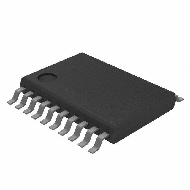
ICGOO电子元器件商城为您提供SN74LVC541APWR由Texas Instruments设计生产,在icgoo商城现货销售,并且可以通过原厂、代理商等渠道进行代购。 SN74LVC541APWR价格参考¥1.53-¥1.53。Texas InstrumentsSN74LVC541APWR封装/规格:逻辑 - 缓冲器,驱动器,接收器,收发器, Buffer, Non-Inverting 1 Element 8 Bit per Element 3-State Output 20-TSSOP。您可以下载SN74LVC541APWR参考资料、Datasheet数据手册功能说明书,资料中有SN74LVC541APWR 详细功能的应用电路图电压和使用方法及教程。
SN74LVC541APWR是Texas Instruments推出的一款八路缓冲/驱动器,属于逻辑器件中的缓冲器与驱动器类别。该芯片为非反相型、三态输出的缓冲器,支持宽电压工作范围(1.65V至5.5V),兼容多种逻辑电平,适用于低电压和混合电压系统设计。

其主要应用场景包括:

1. 数字系统中的信号缓冲:在微处理器、FPGA或ASIC与高电容负载之间提供隔离与驱动能力,增强信号完整性,防止负载影响源端信号。

2. 总线驱动应用:作为地址或数据总线的驱动器,驱动多条线路或长距离PCB走线,提升信号驱动能力和抗干扰性能。

3. 存储器接口扩展:用于存储器系统中,增强控制信号或地址信号的驱动能力,确保稳定传输。

4. 工业控制与通信设备:广泛应用于PLC、工控模块、通信基站等对稳定性和可靠性要求较高的环境。

5. 消费类电子产品:如显示器模块、智能家居控制板等,实现电平转换与信号隔离。

SN74LVC541APWR采用TSSOP-20封装,体积小,适合高密度PCB布局。其三态输出功能允许多个器件共享同一总线,避免信号冲突。此外,低功耗和高噪声抑制能力使其在电池供电设备中也具备良好表现。

综上,该器件适用于需要信号隔离、增强驱动能力及电平兼容的数字系统,广泛用于工业、通信、消费电子等领域。
| 参数 | 数值 |
| 产品目录 | 集成电路 (IC)半导体 |
| 描述 | IC BUFF/DVR TRI-ST 8BIT 20TSSOP缓冲器和线路驱动器 Tri-State Octal |
| 产品分类 | |
| 品牌 | Texas Instruments |
| 产品手册 | |
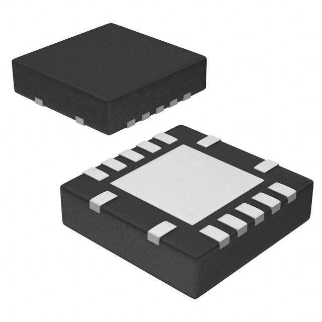
| 产品图片 |
|
| rohs | 符合RoHS无铅 / 符合限制有害物质指令(RoHS)规范要求 |
| 产品系列 | 逻辑集成电路,缓冲器和线路驱动器,Texas Instruments SN74LVC541APWR74LVC |
| 数据手册 | |
| 产品型号 | SN74LVC541APWR |
| 产品目录页面 | |
| 产品种类 | 缓冲器和线路驱动器 |
| 传播延迟时间 | 5.6 ns at 2.7 V, 5.1 ns at 3.3 V |
| 低电平输出电流 | 24 mA |
| 供应商器件封装 | 20-TSSOP |
| 元件数 | 1 |
| 其它名称 | 296-8521-1 |
| 包装 | 剪切带 (CT) |
| 单位重量 | 77 mg |
| 商标 | Texas Instruments |
| 安装类型 | 表面贴装 |
| 安装风格 | SMD/SMT |
| 封装 | Reel |
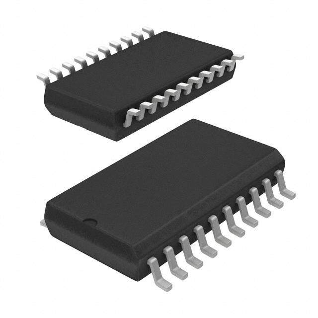
| 封装/外壳 | 20-TSSOP(0.173",4.40mm 宽) |
| 封装/箱体 | TSSOP-20 |
| 工作温度 | -40°C ~ 85°C |
| 工厂包装数量 | 2000 |
| 最大工作温度 | + 85 C |
| 最小工作温度 | - 40 C |
| 极性 | Non-Inverting |
| 标准包装 | 1 |
| 每元件位数 | 8 |
| 每芯片的通道数量 | 8 |
| 电压-电源 | 1.65 V ~ 3.6 V |
| 电流-输出高,低 | 24mA,24mA |
| 电源电压-最大 | 3.6 V |
| 电源电压-最小 | 1.65 V |
| 电源电流 | 0.01 mA |
| 系列 | SN74LVC541A |
| 输入线路数量 | 8 |
| 输出类型 | 3-State |
| 输出线路数量 | 3 |
| 逻辑类型 | 缓冲器/线路驱动器,非反相 |
| 逻辑系列 | LVC |
| 高电平输出电流 | - 24 mA |


- 商务部:美国ITC正式对集成电路等产品启动337调查
- 曝三星4nm工艺存在良率问题 高通将骁龙8 Gen1或转产台积电
- 太阳诱电将投资9.5亿元在常州建新厂生产MLCC 预计2023年完工
- 英特尔发布欧洲新工厂建设计划 深化IDM 2.0 战略
- 台积电先进制程称霸业界 有大客户加持明年业绩稳了
- 达到5530亿美元!SIA预计今年全球半导体销售额将创下新高
- 英特尔拟将自动驾驶子公司Mobileye上市 估值或超500亿美元
- 三星加码芯片和SET,合并消费电子和移动部门,撤换高东真等 CEO
- 三星电子宣布重大人事变动 还合并消费电子和移动部门
- 海关总署:前11个月进口集成电路产品价值2.52万亿元 增长14.8%


PDF Datasheet 数据手册内容提取
Product Sample & Technical Tools & Support & Folder Buy Documents Software Community SN54LVC541A,SN74LVC541A SCAS298N–JANUARY1993–REVISEDJUNE2014 SNx4LVC541A Octal Buffers/Drivers With 3-State Outputs 1 Features 2 Applications • OperateFrom1.65Vto3.6V • Servers 1 • InputsAcceptVoltagesto5.5V • PCsandNotebooks • Maxt of5.1nsat3.3V • NetworkSwitches pd • TypicalV (OutputGroundBounce) • WearableHealthandWellnessDevices OLP <0.8VatVCC=3.3V,TA=25°C • TelecomInfrastructures • TypicalVOHV(OutputVOH Undershoot) • ElectronicPointsofSale >2VatV =3.3V,T =25°C CC A • SupportMixed-ModeSignalOperationon 3 Description AllPorts(5-VInput/OutputVoltageWith The SN54LVC541A octal buffer/driver is designed for 3.3-VV ) 2.7-V to 3.6-V V operation, and the SN74LVC541A CC CC octal buffer/driver is designed for 1.65-V to 3.6-V V • I SupportsLiveInsertion,Partial-Power-Down CC off operation. Mode,andBack-DriveProtection • Latch-UpPerformanceExceeds250mA DeviceInformation(1) PerJESD17 PARTNUMBER PACKAGE BODYSIZE(NOM) • ESDProtectionExceedsJESD22 SSOP(20) 7.20mm×5.30mm – 2000-VHuman-BodyModel(A114-A) TVSOP(20) 5.00mm×4.40mm – 200-VMachineModel(A115-A) SN74LVC541A VQFN(20) 4.50mm×3.50mm – 1000-VCharged-DeviceModel(C101) SOIC(20) 12.80mm×7.50mm • OnProductsComplianttoMIL-PRF-38535, TSSOP(20) 6.50mm×4.40mm AllParametersAreTestedUnlessOtherwise (1) For all available packages, see the orderable addendum at Noted.OnAllOtherProducts,Production theendofthedatasheet. ProcessingDoesNotNecessarilyIncludeTesting ofAllParameters. 4 Simplified Schematic 1 OE1 19 OE2 2 18 A1 Y1 To Seven Other Channels 1 An IMPORTANT NOTICE at the end of this data sheet addresses availability, warranty, changes, use in safety-critical applications, intellectualpropertymattersandotherimportantdisclaimers.PRODUCTIONDATA.
SN54LVC541A,SN74LVC541A SCAS298N–JANUARY1993–REVISEDJUNE2014 www.ti.com Table of Contents 1 Features.................................................................. 1 9 DetailedDescription............................................ 10 2 Applications........................................................... 1 9.1 Overview.................................................................10 3 Description............................................................. 1 9.2 FunctionalBlockDiagram.......................................10 4 SimplifiedSchematic............................................. 1 9.3 FeatureDescription.................................................10 9.4 DeviceFunctionalModes........................................10 5 RevisionHistory..................................................... 2 10 ApplicationandImplementation........................ 11 6 PinConfigurationandFunctions......................... 3 10.1 ApplicationInformation..........................................11 7 Specifications......................................................... 4 10.2 TypicalApplication ...............................................11 7.1 AbsoluteMaximumRatings .....................................4 11 PowerSupplyRecommendations..................... 12 7.2 HandlingRatings.......................................................4 12 Layout................................................................... 12 7.3 RecommendedOperatingConditions......................5 7.4 ThermalInformation..................................................5 12.1 LayoutGuidelines.................................................12 7.5 ElectricalCharacteristics—DCLimitChanges..........6 12.2 LayoutExample....................................................12 7.6 SwitchingCharacteristics—ACLimitChanges.........7 13 DeviceandDocumentationSupport................. 13 7.7 SwitchingCharacteristics,SN74LVC541A–40°Cto 13.1 RelatedLinks........................................................13 85°C........................................................................... 7 13.2 Trademarks...........................................................13 7.8 SwitchingCharacteristics,SN74LVC541A–40°Cto 13.3 ElectrostaticDischargeCaution............................13 125°C.........................................................................7 13.4 Glossary................................................................13 7.9 OperatingCharacteristics..........................................7 14 Mechanical,Packaging,andOrderable 7.10 TypicalCharacteristics............................................8 Information........................................................... 13 8 ParameterMeasurementInformation..................9 5 Revision History NOTE:Pagenumbersforpreviousrevisionsmaydifferfrompagenumbersinthecurrentversion. ChangesfromRevisionM(May2005)toRevisionN Page • UpdateddocumenttonewTIdatasheetformat.................................................................................................................... 1 • RemovedOrderingInformationtable..................................................................................................................................... 1 • UpdatedI Featurebullet...................................................................................................................................................... 1 off • UpdatedFeaturestoincludeMilitaryDisclaimer.................................................................................................................... 1 • AddedApplications ................................................................................................................................................................ 1 • AddedDeviceInformationtable............................................................................................................................................. 1 • AddedHandlingRatingstable................................................................................................................................................ 4 • ChangedMAXoperatingfree-airtemperaturefrom85°Cto125°CforSN74LVC541A........................................................ 5 • UpdatedThermalInformationtable. ...................................................................................................................................... 5 • Added–40°CTO125°CtemperaturerangetoElectricalCharacteristicstableforSN74LVC541A...................................... 6 • AddedSwitchingCharacteristicstable–40°CTO125°CtemperaturerangeforSN74LVC541A......................................... 7 • AddedTypicalCharacteristics................................................................................................................................................ 8 2 SubmitDocumentationFeedback Copyright©1993–2014,TexasInstrumentsIncorporated ProductFolderLinks:SN54LVC541A SN74LVC541A
SN54LVC541A,SN74LVC541A www.ti.com SCAS298N–JANUARY1993–REVISEDJUNE2014 6 Pin Configuration and Functions SN54LVC541A...J OR W PACKAGE SN74LVC541A...RGYPACKAGE SN54LVC541A...FK PACKAGE SN74LVC541A...DB, DGV, DW, NS, (TOPVIEW) (TOPVIEW) OR PW PACKAGE 1 C (TOPVIEW) OE VC 1 C2 2 1 E CE OE1 1 20 VCC 1 20 A A OV O A1 2 19 OE2 A1 2 19 OE2 A2 3 18 Y1 A2 3 18 Y1 3 2 1 20 19 A3 4 17 Y2 A3 4 17 Y2 A3 4 18 Y1 A4 5 16 Y3 A4 5 16 Y3 A4 5 17 Y2 A5 6 15 Y4 A5 6 15 Y4 A6 7 14 Y5 A6 7 14 Y5 A5 6 16 Y3 A7 8 13 Y6 A7 8 13 Y6 A6 7 15 Y4 A8 9 12 Y7 A8 9 12 Y7 A7 8 14 Y5 GND 10 11 Y8 10 11 9 10 11 12 13 D 8 N Y G 8 D 87 6 A N YY Y G PinFunctions PIN I/O DESCRIPTION NO. NAME 1 OE1 I Outputenable 2 A1 I A1input 3 A2 I A2input 4 A3 I A3input 5 A4 I A4input 6 A5 I A5input 7 A6 I A6input 8 A7 I A7input 9 A8 I A8input 10 GND — Groundpin 11 Y8 O Y8output 12 Y7 O Y7output 13 Y6 O Y6output 14 Y5 O Y5output 15 Y4 O Y4output 16 Y3 O Y3output 17 Y2 O Y2output 18 Y1 O Y1output 19 OE2 I Outputenable 20 VCC — Powerpin Copyright©1993–2014,TexasInstrumentsIncorporated SubmitDocumentationFeedback 3 ProductFolderLinks:SN54LVC541A SN74LVC541A
SN54LVC541A,SN74LVC541A SCAS298N–JANUARY1993–REVISEDJUNE2014 www.ti.com 7 Specifications 7.1 Absolute Maximum Ratings overoperatingfree-airtemperaturerange(unlessotherwisenoted)(1) MIN MAX UNIT V Supplyvoltagerange –0.5 6.5 V CC V Inputvoltagerange(2) –0.5 6.5 V I V Voltagerangeappliedtoanyoutputinthehigh-impedanceorpower-offstate(2) –0.5 6.5 V O V Voltagerangeappliedtoanyoutputinthehighorlowstate(2)(3) –0.5 V +0.5 V O CC I Inputclampcurrent V <0 –50 mA IK I I Outputclampcurrent V <0 –50 mA OK O I Continuousoutputcurrent ±50 mA O ContinuouscurrentthroughV orGND ±100 mA CC (1) StressesbeyondthoselistedunderAbsoluteMaximumRatingsmaycausepermanentdamagetothedevice.Thesearestressratings only,andfunctionaloperationofthedeviceattheseoranyotherconditionsbeyondthoseindicatedunderRecommendedOperating Conditionsisnotimplied.Exposuretoabsolute-maximum-ratedconditionsforextendedperiodsmayaffectdevicereliability. (2) Theinputnegative-voltageandoutputvoltageratingsmaybeexceedediftheinputandoutputcurrentratingsareobserved. (3) ThevalueofV isprovidedintheRecommendedOperatingConditionstable. CC 7.2 Handling Ratings MIN MAX UNIT T Storagetemperaturerange –65 150 °C stg Humanbodymodel(HBM),perANSI/ESDA/JEDECJS-001,all pins(1) 0 2000 V Electrostaticdischarge V (ESD) Chargeddevicemodel(CDM),perJEDECspecification JESD22-C101,allpins(2) 0 1000 (1) JEDECdocumentJEP155statesthat500-VHBMallowssafemanufacturingwithastandardESDcontrolprocess. (2) JEDECdocumentJEP157statesthat250-VCDMallowssafemanufacturingwithastandardESDcontrolprocess. 4 SubmitDocumentationFeedback Copyright©1993–2014,TexasInstrumentsIncorporated ProductFolderLinks:SN54LVC541A SN74LVC541A
SN54LVC541A,SN74LVC541A www.ti.com SCAS298N–JANUARY1993–REVISEDJUNE2014 7.3 Recommended Operating Conditions overoperatingfree-airtemperaturerange(unlessotherwisenoted)(1) SN54LVC541A SN74LVC541A UNIT MIN MAX MIN MAX Operating 2 3.6 1.65 3.6 V Supplyvoltage V CC Dataretentiononly 1.5 1.5 V =1.65Vto1.95V 0.65×V CC CC V High-levelinputvoltage V =2.3Vto2.7V 1.7 V IH CC V =2.7Vto3.6V 2 2 CC V =1.65Vto1.95V 0.35×V CC CC V Low-levelinputvoltage V =2.3Vto2.7V 0.7 V IL CC V =2.7Vto3.6V 0.8 0.8 CC V Inputvoltage 0 5.5 0 5.5 V I Highorlowstate 0 V 0 V CC CC V Outputvoltage V O 3-state 0 5.5 0 5.5 V =1.65V –4 CC V =2.3V –8 CC I High-leveloutputcurrent mA OH V =2.7V –12 –12 CC V =3V –24 –24 CC V =1.65V 4 CC V =2.3V 8 CC I Low-leveloutputcurrent mA OL V =2.7V 12 12 CC V =3V 24 24 CC T Operatingfree-airtemperature –55 125 –40 125 °C A (1) AllunusedinputsofthedevicemustbeheldatV orGNDtoensureproperdeviceoperation.RefertotheTIapplicationreport, CC ImplicationsofSloworFloatingCMOSInputs,literaturenumberSCBA004. 7.4 Thermal Information overoperatingfree-airtemperaturerange(unlessotherwisenoted) SN74LVC541A THERMALMETRIC(1) DB DGV DW NS PW UNIT 20PINS R Junction-to-ambientthermalresistance 112.1 128.9 99.4 90.3 100.8 θJA R Junction-to-case(top)thermalresistance 73.6 43.8 66.9 56.6 35.2 θJC(top) R Junction-to-boardthermalresistance 67.3 70.4 66.9 57.8 51.8 θJB °C/W ψ Junction-to-topcharacterizationparameter 33.3 3.2 33.8 28.7 2.2 JT ψ Junction-to-boardcharacterizationparameter 66.9 69.7 66.5 57.4 51.2 JB R Junction-to-case(bottom)thermalresistance n/a n/a n/a n/a n/a θJC(bot) (1) Formoreinformationabouttraditionalandnewthermalmetrics,seetheICPackageThermalMetricsapplicationreport,literature numberSPRA953. Copyright©1993–2014,TexasInstrumentsIncorporated SubmitDocumentationFeedback 5 ProductFolderLinks:SN54LVC541A SN74LVC541A
SN54LVC541A,SN74LVC541A SCAS298N–JANUARY1993–REVISEDJUNE2014 www.ti.com 7.5 Electrical Characteristics—DC Limit Changes overrecommendedoperatingfree-airtemperaturerange(unlessotherwisenoted) –55°CTO125°C –40°CTO85°C –40°CTO125°C PARAMETER TESTCONDITIONS VCC SN54LVC541A SN74LVC541A SN74LVC541A UNIT MIN TYP(1) MAX MIN TYP(1) MAX MIN TYP(1) MAX 1.65Vto 3.6V VCC–0.2 VCC–0.3 IOH=–100μA 2.7Vto 3.6V VCC–0.2 VOH IOH=–4mA 1.65V 1.20 1.20 V IOH=–8mA 2.3V 1.7 1.7 2.7V 2.2 2.2 2.2 IOH=–12mA 3V 2.4 2.4 2.4 IOH=–24mA 3V 2.2 2.2 2.2 1.65Vto 0.2 0.3 3.6V IOL=100μA 2.7Vto 0.2 3.6V VOL IOL=4mA 1.65V 0.45 0.45 V IOL=8mA 2.3V 0.7 0.7 IOL=12mA 2.7V 0.4 0.4 0.4 IOL=24mA 3V 0.55 0.55 0.55 II VI=0to5.5V 3.6V ±5 ±5 ±5 μA Ioff VIorVO=5.5V 0 ±10 ±10 μA IOZ VO=0to5.5V 3.6V ±15 ±10 ±10 μA VI=VCCorGND 10 10 10 ICC 3.6V≤VI≤5.5V(2) IO=0 3.6V 10 10 10 μA ΔICC OOntheerinipnuptuatstaVtCVCCC–o0r.6GVN,D 2.37.6VVto 500 500 500 μA Ci VI=VCCorGND 3.3V 4 4 4 pF Co VO=VCCorGND 3.3V 5.5 5.5 5.5 pF (1) AlltypicalvaluesareatV =3.3V,T =25°C. CC A (2) Thisappliesinthedisabledstateonly. 6 SubmitDocumentationFeedback Copyright©1993–2014,TexasInstrumentsIncorporated ProductFolderLinks:SN54LVC541A SN74LVC541A
SN54LVC541A,SN74LVC541A www.ti.com SCAS298N–JANUARY1993–REVISEDJUNE2014 7.6 Switching Characteristics—AC Limit Changes overrecommendedoperatingfree-airtemperaturerange(unlessotherwisenoted)(seeFigure3) SN54LVC541A FROM TO PARAMETER V =2.7V V =3.3V±0.3V UNIT (INPUT) (OUTPUT) CC CC MIN MAX MIN MAX t A Y 5.6 1 5.1 ns pd t OE Y 7.5 1 7 ns en t OE Y 7.7 1 7 ns dis 7.7 Switching Characteristics, SN74LVC541A –40°C to 85°C overrecommendedoperatingfree-airtemperaturerange(unlessotherwisenoted)(seeFigure3) SN74LVC541A –40°CTO85°C FROM TO PARAMETER (INPUT) (OUTPUT) VCC=1.8V VCC=2.5V V =2.7V VCC=3.3V UNIT ±0.15V ±0.2V CC ±0.3V MIN MAX MIN MAX MIN MAX MIN MAX t A Y 1 15.7 1 7.8 1 5.6 1.5 5.1 ns pd t OE Y 1 17.5 1 10.5 1 7.5 1.5 7 ns en t OE Y 1 16.5 1 9 1 7.7 1.5 7 ns dis t 1 ns sk(o) 7.8 Switching Characteristics, SN74LVC541A –40°C to 125°C overrecommendedoperatingfree-airtemperaturerange(unlessotherwisenoted)(seeFigure3) SN74LVC541A –40°CTO125°C FROM TO PARAMETER (INPUT) (OUTPUT) VCC=1.8V VCC=2.5V V =2.7V VCC=3.3V UNIT ±0.15V ±0.2V CC ±0.3V MIN MAX MIN MAX MIN MAX MIN MAX t A Y 1 16.3 1 8.3 1 6.1 1 5.6 ns pd t OE Y 1 18.5 1 11.1 1 8 1 7.5 ns en t OE Y 1 17.3 1 9.7 1 8.2 1 7.5 ns dis t 1.5 ns sk(o) 7.9 Operating Characteristics T =25°C A TEST VCC=1.8V VCC=2.5V VCC=3.3V PARAMETER UNIT CONDITIONS TYP TYP TYP Powerdissipationcapacitance Outputsenabled 65 58 33 C f=10MHz pF pd perbuffer/driver Outputsdisabled 2 2 2 Copyright©1993–2014,TexasInstrumentsIncorporated SubmitDocumentationFeedback 7 ProductFolderLinks:SN54LVC541A SN74LVC541A
SN54LVC541A,SN74LVC541A SCAS298N–JANUARY1993–REVISEDJUNE2014 www.ti.com 7.10 Typical Characteristics 6 4 TPD 5.5 3.5 5 4.5 3 4 2.5 s 3.5 s n n D - 3 D - 2 P P T 2.5 T 1.5 2 1.5 1 1 0.5 0.5 TPD 0 0 0 1 2 3 3.5 -100 -50 0 50 100 150 VCC - V D001 Temperature (qC) D002 Figure1.SN74LVC541ATPDAcrossV at25°C Figure2.SN74LVC541ATPDAcrossTemperatureat3.3V CC 8 SubmitDocumentationFeedback Copyright©1993–2014,TexasInstrumentsIncorporated ProductFolderLinks:SN54LVC541A SN74LVC541A
SN54LVC541A,SN74LVC541A www.ti.com SCAS298N–JANUARY1993–REVISEDJUNE2014 8 Parameter Measurement Information VLOAD From Output RL S1 Open TEST S1 Under Test GND tPLH/tPHL Open (see Note CAL) RL tPLZ/tPZL VLOAD tPHZ/tPZH GND LOAD CIRCUIT INPUTS VCC VI tr/tf VM VLOAD CL RL VD 1.8 V ± 0.15 V VCC ≤2 ns VCC/2 2 × VCC 30 pF 1 kW 0.15 V 2.5 V ± 0.2 V VCC ≤2 ns VCC/2 2 × VCC 30 pF 500 W 0.15 V 2.7 V 2.7 V ≤2.5 ns 1.5 V 6 V 50 pF 500 W 0.3 V 3.3 V ± 0.3 V 2.7 V ≤2.5 ns 1.5 V 6 V 50 pF 500 W 0.3 V VI Timing Input VM 0 V tw VI tsu th VI Input VM VM Data Input VM VM 0 V 0 V VOLTAGE WAVEFORMS VOLTAGE WAVEFORMS PULSE DURATION SETUP AND HOLD TIMES VI VI Output Input VM VM Control VM VM 0 V 0 V tPLH tPHL tPZL tPLZ Output VOH Waveform 1 VLOAD/2 Output VM VM VOL (Ss1e ea tN VoLteO ABD) VM VOL + VD VOL tPHL tPLH tPZH tPHZ Output VM VM VOH WSa1v eaOfto uGrtmpNu D2t VM VOH − VD VOH VOL (see Note B) ≈0 V VOLTAGE WAVEFORMS VOLTAGE WAVEFORMS PROPAGATION DELAY TIMES ENABLE AND DISABLE TIMES INVERTING AND NONINVERTING OUTPUTS LOW- AND HIGH-LEVEL ENABLING NOTES: A. CL includes probe and jig capacitance. B. Waveform 1 is for an output with internal conditions such that the output is low, except when disabled by the output control. Waveform2 is for an output with internal conditions such that the output is high, except when disabled by the output control. C. All input pulses are supplied by generators having the following characteristics: PRR ≤ 10 MHz, ZO = 50 W . D. The outputs are measured one at a time, with one transition per measurement. E. tPLZ and tPHZ are the same as tdis. F. tPZL and tPZH are the same as ten. G. tPLH and tPHL are the same as tpd. H. All parameters and waveforms are not applicable to all devices. Figure3. LoadCircuitandVoltageWaveforms Copyright©1993–2014,TexasInstrumentsIncorporated SubmitDocumentationFeedback 9 ProductFolderLinks:SN54LVC541A SN74LVC541A
SN54LVC541A,SN74LVC541A SCAS298N–JANUARY1993–REVISEDJUNE2014 www.ti.com 9 Detailed Description 9.1 Overview The'LVC541Adevicesareidealfordrivingbuslinesorbufferingmemoryaddressregisters. These devices feature inputs and outputs on opposite sides of the package to facilitate printed circuit board layout. The 3-state control gate is a 2-input AND gate with active-low inputs so that, if either output enable (OE1 or OE2) input is high, all eight outputs are in the high-impedance state. Inputs can be driven from either 3.3-V or 5-V devices. This feature allows the use of these devices as translators in a mixed 3.3-V/5-V system environment. These devices are fully specified for partial-power-down applications using I . The I circuitry off off disables the outputs, preventing damaging current backflow through the devices when they are powered down. To ensure the high-impedance state during power up or power down, OE should be tied to V through a pullup CC resistor;theminimumvalueoftheresistorisdeterminedbythecurrent-sinkingcapabilityofthedriver. 9.2 Functional Block Diagram 1 OE1 19 OE2 2 18 A1 Y1 To Seven Other Channels 9.3 Feature Description • Wideoperatingvoltagerange – Operatesfrom1.65Vto3.6V • Allowsdownvoltagetranslation – Inputsacceptvoltagesto5.5V • I feature off – AllowsvoltagesontheinputsandoutputswhenV is0V CC 9.4 Device Functional Modes Table1.FunctionTable INPUTS OUTPUT OE1 OE2 A Y L L L L L L H H H X X Z X H X Z 10 SubmitDocumentationFeedback Copyright©1993–2014,TexasInstrumentsIncorporated ProductFolderLinks:SN54LVC541A SN74LVC541A
SN54LVC541A,SN74LVC541A www.ti.com SCAS298N–JANUARY1993–REVISEDJUNE2014 10 Application and Implementation 10.1 Application Information The SN74LVC541A is a high-drive CMOS device that can be used for a multitude of bus-interface type applications where the data needs to be retained or latched. It can produce 24 mA of drive current at 3.3 V. Therefore, this device is ideal for driving multiple outputs and for high-speed applications up to 100 Mhz. The inputsare5.5VtolerantallowingthedevicetotranslatedowntoV . CC 10.2 Typical Application Regulated 3.3 V OE1 Vcc OE2 A1 Y1 uC System Logic LEDs uC or A8 Y8 System Logic GND Figure4. TypicalApplicationDiagram 10.2.1 DesignRequirements This device uses CMOS technology and has balanced output drive. Care should be taken to avoid bus contention because it can drive currents that would exceed maximum limits. The high drive will also create fast edgesintolightloads;therefore,routingandloadconditionsshouldbeconsideredtopreventringing. 10.2.2 DetailedDesignProcedure 1. RecommendedInputConditions – Risetimeandfalltimespecs:See(Δt/ΔV)intheRecommendedOperatingConditionstable. – Specifiedhighandlowlevels:See(V andV )intheRecommendedOperatingConditions table. IH IL – Inputsareovervoltagetolerantallowingthemtogoashighas5.5VatanyvalidV . CC 2. RecommendOutputConditions – Loadcurrentsshouldnotexceed25mAperoutputand50mAtotalforthepart. – OutputsshouldnotbepulledaboveV . CC Copyright©1993–2014,TexasInstrumentsIncorporated SubmitDocumentationFeedback 11 ProductFolderLinks:SN54LVC541A SN74LVC541A
SN54LVC541A,SN74LVC541A SCAS298N–JANUARY1993–REVISEDJUNE2014 www.ti.com Typical Application (continued) 10.2.3 ApplicationCurves 300 ICC 1.8 V ICC 2.5 V 250 ICC 3.3 V 200 A m - C 150 C I 100 50 0 0 10 20 30 40 50 60 Frequency D003 Figure5.I vsFrequency CC 11 Power Supply Recommendations The power supply can be any voltage between the MIN and MAX supply voltage rating located in the RecommendedOperatingConditionstable. Each V pin should have a good bypass capacitor to prevent power disturbance. For devices with a single CC supply, 0.1 μf is recommended; if there are multiple V pins, then 0.01 μf or 0.022 μf is recommended for each CC power pin. It is acceptable to parallel multiple bypass caps to reject different frequencies of noise. A 0.1 μf and a 1 μf are commonly used in parallel. The bypass capacitor should be installed as close to the power pin as possibleforbestresults. 12 Layout 12.1 Layout Guidelines Whenusingmultiplebitlogicdevicesinputsshouldneverfloat. In many cases, functions or parts of functions of digital logic devices are unused, for example, when only two inputs of a triple-input AND gate are used or only 3 of the 4 buffer gates are used. Such input pins should not be left unconnected because the undefined voltages at the outside connections result in undefined operational states. Figure 6 specifies the rules that must be observed under all circumstances. All unused inputs of digital logic devices must be connected to a high or low bias to prevent them from floating. The logic level that should be applied to any particular unused input depends on the function of the device. Generally they will be tied to GND or V whichever make more sense or is more convenient. It is generally acceptable to float outputs, CC unlessthepartisatransceiver.Ifthetransceiverhasanoutputenablepin,itwilldisabletheoutputsectionofthe partwhenasserted.ThiswillnotdisabletheinputsectionoftheI/Os,sotheycannotfloatwhendisabled. 12.2 Layout Example V cc Input Unused Input Output Unused Input Output Input Figure6. LayoutDiagram 12 SubmitDocumentationFeedback Copyright©1993–2014,TexasInstrumentsIncorporated ProductFolderLinks:SN54LVC541A SN74LVC541A
SN54LVC541A,SN74LVC541A www.ti.com SCAS298N–JANUARY1993–REVISEDJUNE2014 13 Device and Documentation Support 13.1 Related Links The table below lists quick access links. Categories include technical documents, support and community resources,toolsandsoftware,andquickaccesstosampleorbuy. Table2.RelatedLinks TECHNICAL TOOLS& SUPPORT& PARTS PRODUCTFOLDER SAMPLE&BUY DOCUMENTS SOFTWARE COMMUNITY SN54LVC541A Clickhere Clickhere Clickhere Clickhere Clickhere SN74LVC541A Clickhere Clickhere Clickhere Clickhere Clickhere 13.2 Trademarks Alltrademarksarethepropertyoftheirrespectiveowners. 13.3 Electrostatic Discharge Caution Thesedeviceshavelimitedbuilt-inESDprotection.Theleadsshouldbeshortedtogetherorthedeviceplacedinconductivefoam duringstorageorhandlingtopreventelectrostaticdamagetotheMOSgates. 13.4 Glossary SLYZ022—TIGlossary. Thisglossarylistsandexplainsterms,acronymsanddefinitions. 14 Mechanical, Packaging, and Orderable Information The following pages include mechanical, packaging, and orderable information. This information is the most current data available for the designated devices. This data is subject to change without notice and revision of thisdocument.Forbrowser-basedversionsofthisdatasheet,refertotheleft-handnavigation. Copyright©1993–2014,TexasInstrumentsIncorporated SubmitDocumentationFeedback 13 ProductFolderLinks:SN54LVC541A SN74LVC541A
PACKAGE OPTION ADDENDUM www.ti.com 6-Feb-2020 PACKAGING INFORMATION Orderable Device Status Package Type Package Pins Package Eco Plan Lead/Ball Finish MSL Peak Temp Op Temp (°C) Device Marking Samples (1) Drawing Qty (2) (6) (3) (4/5) 5962-9759501Q2A ACTIVE LCCC FK 20 1 TBD POST-PLATE N / A for Pkg Type -55 to 125 5962- 9759501Q2A SNJ54LVC 541AFK 5962-9759501QRA ACTIVE CDIP J 20 1 TBD Call TI N / A for Pkg Type -55 to 125 5962-9759501QR A SNJ54LVC541AJ 5962-9759501QSA ACTIVE CFP W 20 1 TBD Call TI N / A for Pkg Type -55 to 125 5962-9759501QS A SNJ54LVC541AW SN74LVC541ADBR ACTIVE SSOP DB 20 2000 Green (RoHS NIPDAU Level-1-260C-UNLIM -40 to 125 LC541A & no Sb/Br) SN74LVC541ADBRG4 ACTIVE SSOP DB 20 2000 Green (RoHS NIPDAU Level-1-260C-UNLIM -40 to 125 LC541A & no Sb/Br) SN74LVC541ADGVR ACTIVE TVSOP DGV 20 2000 Green (RoHS NIPDAU Level-1-260C-UNLIM -40 to 125 LC541A & no Sb/Br) SN74LVC541ADGVRE4 ACTIVE TVSOP DGV 20 2000 Green (RoHS NIPDAU Level-1-260C-UNLIM -40 to 125 LC541A & no Sb/Br) SN74LVC541ADGVRG4 ACTIVE TVSOP DGV 20 2000 Green (RoHS NIPDAU Level-1-260C-UNLIM -40 to 125 LC541A & no Sb/Br) SN74LVC541ADW ACTIVE SOIC DW 20 25 Green (RoHS NIPDAU Level-1-260C-UNLIM -40 to 125 LVC541A & no Sb/Br) SN74LVC541ADWR ACTIVE SOIC DW 20 2000 Green (RoHS NIPDAU Level-1-260C-UNLIM -40 to 125 LVC541A & no Sb/Br) SN74LVC541ADWRE4 ACTIVE SOIC DW 20 2000 Green (RoHS NIPDAU Level-1-260C-UNLIM -40 to 125 LVC541A & no Sb/Br) SN74LVC541ANSR ACTIVE SO NS 20 2000 Green (RoHS NIPDAU Level-1-260C-UNLIM -40 to 125 LVC541A & no Sb/Br) SN74LVC541APW ACTIVE TSSOP PW 20 70 Green (RoHS NIPDAU Level-1-260C-UNLIM -40 to 125 LC541A & no Sb/Br) SN74LVC541APWG4 ACTIVE TSSOP PW 20 70 Green (RoHS NIPDAU Level-1-260C-UNLIM -40 to 125 LC541A & no Sb/Br) SN74LVC541APWR ACTIVE TSSOP PW 20 2000 Green (RoHS NIPDAU | SN Level-1-260C-UNLIM -40 to 125 LC541A & no Sb/Br) Addendum-Page 1
PACKAGE OPTION ADDENDUM www.ti.com 6-Feb-2020 Orderable Device Status Package Type Package Pins Package Eco Plan Lead/Ball Finish MSL Peak Temp Op Temp (°C) Device Marking Samples (1) Drawing Qty (2) (6) (3) (4/5) SN74LVC541APWRE4 ACTIVE TSSOP PW 20 2000 Green (RoHS NIPDAU Level-1-260C-UNLIM -40 to 125 LC541A & no Sb/Br) SN74LVC541APWRG4 ACTIVE TSSOP PW 20 2000 Green (RoHS NIPDAU Level-1-260C-UNLIM -40 to 125 LC541A & no Sb/Br) SN74LVC541APWT ACTIVE TSSOP PW 20 250 Green (RoHS NIPDAU Level-1-260C-UNLIM -40 to 125 LC541A & no Sb/Br) SN74LVC541ARGYR ACTIVE VQFN RGY 20 3000 Green (RoHS NIPDAU Level-2-260C-1 YEAR -40 to 125 LC541A & no Sb/Br) SN74LVC541ARGYRG4 ACTIVE VQFN RGY 20 3000 Green (RoHS NIPDAU Level-2-260C-1 YEAR -40 to 125 LC541A & no Sb/Br) SNJ54LVC541AFK ACTIVE LCCC FK 20 1 TBD POST-PLATE N / A for Pkg Type -55 to 125 5962- 9759501Q2A SNJ54LVC 541AFK SNJ54LVC541AJ ACTIVE CDIP J 20 1 TBD Call TI N / A for Pkg Type -55 to 125 5962-9759501QR A SNJ54LVC541AJ SNJ54LVC541AW ACTIVE CFP W 20 1 TBD Call TI N / A for Pkg Type -55 to 125 5962-9759501QS A SNJ54LVC541AW (1) The marketing status values are defined as follows: ACTIVE: Product device recommended for new designs. LIFEBUY: TI has announced that the device will be discontinued, and a lifetime-buy period is in effect. NRND: Not recommended for new designs. Device is in production to support existing customers, but TI does not recommend using this part in a new design. PREVIEW: Device has been announced but is not in production. Samples may or may not be available. OBSOLETE: TI has discontinued the production of the device. (2) RoHS: TI defines "RoHS" to mean semiconductor products that are compliant with the current EU RoHS requirements for all 10 RoHS substances, including the requirement that RoHS substance do not exceed 0.1% by weight in homogeneous materials. Where designed to be soldered at high temperatures, "RoHS" products are suitable for use in specified lead-free processes. TI may reference these types of products as "Pb-Free". RoHS Exempt: TI defines "RoHS Exempt" to mean products that contain lead but are compliant with EU RoHS pursuant to a specific EU RoHS exemption. Green: TI defines "Green" to mean the content of Chlorine (Cl) and Bromine (Br) based flame retardants meet JS709B low halogen requirements of <=1000ppm threshold. Antimony trioxide based flame retardants must also meet the <=1000ppm threshold requirement. (3) MSL, Peak Temp. - The Moisture Sensitivity Level rating according to the JEDEC industry standard classifications, and peak solder temperature. (4) There may be additional marking, which relates to the logo, the lot trace code information, or the environmental category on the device. Addendum-Page 2
PACKAGE OPTION ADDENDUM www.ti.com 6-Feb-2020 (5) Multiple Device Markings will be inside parentheses. Only one Device Marking contained in parentheses and separated by a "~" will appear on a device. If a line is indented then it is a continuation of the previous line and the two combined represent the entire Device Marking for that device. (6) Lead/Ball Finish - Orderable Devices may have multiple material finish options. Finish options are separated by a vertical ruled line. Lead/Ball Finish values may wrap to two lines if the finish value exceeds the maximum column width. Important Information and Disclaimer:The information provided on this page represents TI's knowledge and belief as of the date that it is provided. TI bases its knowledge and belief on information provided by third parties, and makes no representation or warranty as to the accuracy of such information. Efforts are underway to better integrate information from third parties. TI has taken and continues to take reasonable steps to provide representative and accurate information but may not have conducted destructive testing or chemical analysis on incoming materials and chemicals. TI and TI suppliers consider certain information to be proprietary, and thus CAS numbers and other limited information may not be available for release. In no event shall TI's liability arising out of such information exceed the total purchase price of the TI part(s) at issue in this document sold by TI to Customer on an annual basis. OTHER QUALIFIED VERSIONS OF SN54LVC541A, SN74LVC541A : •Catalog: SN74LVC541A •Automotive: SN74LVC541A-Q1, SN74LVC541A-Q1 •Enhanced Product: SN74LVC541A-EP, SN74LVC541A-EP •Military: SN54LVC541A NOTE: Qualified Version Definitions: •Catalog - TI's standard catalog product •Automotive - Q100 devices qualified for high-reliability automotive applications targeting zero defects •Enhanced Product - Supports Defense, Aerospace and Medical Applications •Military - QML certified for Military and Defense Applications Addendum-Page 3
PACKAGE MATERIALS INFORMATION www.ti.com 17-Apr-2020 TAPE AND REEL INFORMATION *Alldimensionsarenominal Device Package Package Pins SPQ Reel Reel A0 B0 K0 P1 W Pin1 Type Drawing Diameter Width (mm) (mm) (mm) (mm) (mm) Quadrant (mm) W1(mm) SN74LVC541ADBR SSOP DB 20 2000 330.0 16.4 8.2 7.5 2.5 12.0 16.0 Q1 SN74LVC541ADGVR TVSOP DGV 20 2000 330.0 12.4 6.9 5.6 1.6 8.0 12.0 Q1 SN74LVC541ADWR SOIC DW 20 2000 330.0 24.4 10.8 13.3 2.7 12.0 24.0 Q1 SN74LVC541ANSR SO NS 20 2000 330.0 24.4 8.4 13.0 2.5 12.0 24.0 Q1 SN74LVC541APWR TSSOP PW 20 2000 330.0 16.4 6.95 7.1 1.6 8.0 16.0 Q1 SN74LVC541APWR TSSOP PW 20 2000 330.0 16.4 6.95 7.0 1.4 8.0 16.0 Q1 SN74LVC541APWT TSSOP PW 20 250 330.0 16.4 6.95 7.1 1.6 8.0 16.0 Q1 SN74LVC541ARGYR VQFN RGY 20 3000 330.0 12.4 3.8 4.8 1.6 8.0 12.0 Q1 PackMaterials-Page1
PACKAGE MATERIALS INFORMATION www.ti.com 17-Apr-2020 *Alldimensionsarenominal Device PackageType PackageDrawing Pins SPQ Length(mm) Width(mm) Height(mm) SN74LVC541ADBR SSOP DB 20 2000 367.0 367.0 38.0 SN74LVC541ADGVR TVSOP DGV 20 2000 367.0 367.0 35.0 SN74LVC541ADWR SOIC DW 20 2000 367.0 367.0 45.0 SN74LVC541ANSR SO NS 20 2000 367.0 367.0 45.0 SN74LVC541APWR TSSOP PW 20 2000 364.0 364.0 27.0 SN74LVC541APWR TSSOP PW 20 2000 367.0 367.0 38.0 SN74LVC541APWT TSSOP PW 20 250 367.0 367.0 38.0 SN74LVC541ARGYR VQFN RGY 20 3000 367.0 367.0 35.0 PackMaterials-Page2
None
None
PACKAGE OUTLINE DB0020A SSOP - 2 mm max height SCALE 2.000 SMALL OUTLINE PACKAGE C 8.2 TYP 7.4 A 0.1 C PIN 1 INDEX AREA SEATING PLANE 18X 0.65 20 1 2X 7.5 5.85 6.9 NOTE 3 10 11 0.38 20X 0.22 5.6 B 0.1 C A B 5.0 NOTE 4 2 MAX (0.15) TYP 0.25 SEE DETAIL A GAGE PLANE 0 -8 0.95 0.05 MIN 0.55 DETA 15AIL A TYPICAL 4214851/B 08/2019 NOTES: 1. All linear dimensions are in millimeters. Any dimensions in parenthesis are for reference only. Dimensioning and tolerancing per ASME Y14.5M. 2. This drawing is subject to change without notice. 3. This dimension does not include mold flash, protrusions, or gate burrs. Mold flash, protrusions, or gate burrs shall not exceed 0.15 mm per side. 4. This dimension does not include interlead flash. Interlead flash shall not exceed 0.25 mm per side. 5. Reference JEDEC registration MO-150. www.ti.com
EXAMPLE BOARD LAYOUT DB0020A SSOP - 2 mm max height SMALL OUTLINE PACKAGE 20X (1.85) SYMM (R0.05) TYP 1 20X (0.45) 20 SYMM 18X (0.65) 10 11 (7) LAND PATTERN EXAMPLE EXPOSED METAL SHOWN SCALE: 10X SOLDER MASK METAL METAL UNDER SOLDER MASK OPENING SOLDER MASK OPENING EXPOSED METAL EXPOSED METAL 0.07 MAX 0.07 MIN ALL AROUND ALL AROUND NON-SOLDER MASK SOLDER MASK DEFINED DEFINED (PREFERRED) SOLDE15.000 R MASK DETAILS 4214851/B 08/2019 NOTES: (continued) 6. Publication IPC-7351 may have alternate designs. 7. Solder mask tolerances between and around signal pads can vary based on board fabrication site. www.ti.com
EXAMPLE STENCIL DESIGN DB0020A SSOP - 2 mm max height SMALL OUTLINE PACKAGE 20X (1.85) SYMM (R0.05) TYP 1 20X (0.45) 20 SYMM 18X (0.65) 10 11 (7) SOLDER PASTE EXAMPLE BASED ON 0.125 mm THICK STENCIL SCALE: 10X 4214851/B 08/2019 NOTES: (continued) 8. Laser cutting apertures with trapezoidal walls and rounded corners may offer better paste release. IPC-7525 may have alternate design recommendations. 9. Board assembly site may have different recommendations for stencil design. www.ti.com
None
None
MECHANICAL DATA MPDS006C – FEBRUARY 1996 – REVISED AUGUST 2000 DGV (R-PDSO-G**) PLASTIC SMALL-OUTLINE 24 PINS SHOWN 0,23 0,40 0,07 M 0,13 24 13 0,16 NOM 4,50 6,60 4,30 6,20 Gage Plane 0,25 0°–(cid:1)8° 0,75 1 12 0,50 A Seating Plane 0,15 1,20 MAX 0,08 0,05 PINS ** 14 16 20 24 38 48 56 DIM A MAX 3,70 3,70 5,10 5,10 7,90 9,80 11,40 A MIN 3,50 3,50 4,90 4,90 7,70 9,60 11,20 4073251/E 08/00 NOTES: A. All linear dimensions are in millimeters. B. This drawing is subject to change without notice. C. Body dimensions do not include mold flash or protrusion, not to exceed 0,15 per side. D. Falls within JEDEC: 24/48 Pins – MO-153 14/16/20/56 Pins – MO-194 • POST OFFICE BOX 655303 DALLAS, TEXAS 75265
None
None
GENERIC PACKAGE VIEW RGY 20 VQFN - 1 mm max height 3.5 x 4.5, 0.5 mm pitch PLASTIC QUAD FGLATPACK - NO LEAD This image is a representation of the package family, actual package may vary. Refer to the product data sheet for package details. 4225264/A www.ti.com
PACKAGE OUTLINE RGY0020A VQFN - 1 mm max height SCALE 3.000 PLASTIC QUAD FLATPACK - NO LEAD A 3.65 B 3.35 PIN 1 INDEX AREA 4.65 4.35 1.0 0.8 C SEATING PLANE 0.05 0.00 0.08 C 2.05 0.1 2X 1.5 (0.2) TYP 10 11 EXPOSED THERMAL PAD 9 12 14X 0.5 2X SYMM 21 3.05 0.1 3.5 2 19 0.30 PIN 1 ID 1 20 20X 0.18 SYMM 0.1 C A B 0.5 0.05 20X 0.3 4225320/A 09/2019 NOTES: 1. All linear dimensions are in millimeters. Any dimensions in parenthesis are for reference only. Dimensioning and tolerancing per ASME Y14.5M. 2. This drawing is subject to change without notice. 3. The package thermal pad must be soldered to the printed circuit board for thermal and mechanical performance. www.ti.com
EXAMPLE BOARD LAYOUT RGY0020A VQFN - 1 mm max height PLASTIC QUAD FLATPACK - NO LEAD (2.05) SYMM 1 20 20X (0.6) 2 19 20X (0.24) (1.275) (4.3) SYMM 21 (3.05) 14X (0.5) (0.775) 9 12 (R0.05) TYP ( 0.2) TYP VIA 10 11 (0.75) TYP (3.3) LAND PATTERN EXAMPLE EXPOSED METAL SHOWN SCALE:18X 0.07 MAX 0.07 MIN ALL AROUND ALL AROUND SOLDER MASK METAL OPENING EXPOSED METAL SOLDER MASK EXPOSED METAL UNDER OPENING METAL SOLDER MASK NON SOLDER MASK SOLDER MASK DEFINED DEFINED (PREFERRED) SOLDER MASK DETAILS 4225320/A 09/2019 NOTES: (continued) 4. This package is designed to be soldered to a thermal pad on the board. For more information, see Texas Instruments literature number SLUA271 (www.ti.com/lit/slua271). 5. Vias are optional depending on application, refer to device data sheet. If any vias are implemented, refer to their locations shown on this view. It is recommended that vias under paste be filled, plugged or tented. www.ti.com
EXAMPLE STENCIL DESIGN RGY0020A VQFN - 1 mm max height PLASTIC QUAD FLATPACK - NO LEAD SYMM 4X (0.92) 1 20 (R0.05) TYP 20X (0.6) 2 19 20X (0.24) 4X (1.33) 21 SYMM (4.3) (0.77) 14X (0.5) (0.56) 9 12 METAL TYP 10 11 (0.75) TYP (3.3) SOLDER PASTE EXAMPLE BASED ON 0.125 mm THICK STENCIL EXPOSED PAD 21 78% PRINTED SOLDER COVERAGE BY AREA UNDER PACKAGE SCALE:20X 4225320/A 09/2019 NOTES: (continued) 6. Laser cutting apertures with trapezoidal walls and rounded corners may offer better paste release. IPC-7525 may have alternate design recommendations. www.ti.com
PACKAGE OUTLINE DW0020A SOIC - 2.65 mm max height SCALE 1.200 SOIC C 10.63 SEATING PLANE TYP 9.97 A PIN 1 ID 0.1 C AREA 18X 1.27 20 1 13.0 2X 12.6 11.43 NOTE 3 10 11 0.51 20X 7.6 0.31 2.65 MAX B 7.4 0.25 C A B NOTE 4 0.33 TYP 0.10 0.25 SEE DETAIL A GAGE PLANE 0.3 1.27 0 - 8 0.1 0.40 DETAIL A TYPICAL 4220724/A 05/2016 NOTES: 1. All linear dimensions are in millimeters. Dimensions in parenthesis are for reference only. Dimensioning and tolerancing per ASME Y14.5M. 2. This drawing is subject to change without notice. 3. This dimension does not include mold flash, protrusions, or gate burrs. Mold flash, protrusions, or gate burrs shall not exceed 0.15 mm per side. 4. This dimension does not include interlead flash. Interlead flash shall not exceed 0.43 mm per side. 5. Reference JEDEC registration MS-013. www.ti.com
EXAMPLE BOARD LAYOUT DW0020A SOIC - 2.65 mm max height SOIC 20X (2) SYMM 1 20 20X (0.6) 18X (1.27) SYMM (R0.05) TYP 10 11 (9.3) LAND PATTERN EXAMPLE SCALE:6X SOOPLEDNEINRG MASK METAL MSOELTDAEL RU NMDAESRK SOOPLEDNEINRG MASK 0.07 MAX 0.07 MIN ALL AROUND ALL AROUND NON SOLDER MASK SOLDER MASK DEFINED DEFINED SOLDER MASK DETAILS 4220724/A 05/2016 NOTES: (continued) 6. Publication IPC-7351 may have alternate designs. 7. Solder mask tolerances between and around signal pads can vary based on board fabrication site. www.ti.com
EXAMPLE STENCIL DESIGN DW0020A SOIC - 2.65 mm max height SOIC 20X (2) SYMM 1 20 20X (0.6) 18X (1.27) SYMM 10 11 (9.3) SOLDER PASTE EXAMPLE BASED ON 0.125 mm THICK STENCIL SCALE:6X 4220724/A 05/2016 NOTES: (continued) 8. Laser cutting apertures with trapezoidal walls and rounded corners may offer better paste release. IPC-7525 may have alternate design recommendations. 9. Board assembly site may have different recommendations for stencil design. www.ti.com
IMPORTANTNOTICEANDDISCLAIMER TI PROVIDES TECHNICAL AND RELIABILITY DATA (INCLUDING DATASHEETS), DESIGN RESOURCES (INCLUDING REFERENCE DESIGNS), APPLICATION OR OTHER DESIGN ADVICE, WEB TOOLS, SAFETY INFORMATION, AND OTHER RESOURCES “AS IS” AND WITH ALL FAULTS, AND DISCLAIMS ALL WARRANTIES, EXPRESS AND IMPLIED, INCLUDING WITHOUT LIMITATION ANY IMPLIED WARRANTIES OF MERCHANTABILITY, FITNESS FOR A PARTICULAR PURPOSE OR NON-INFRINGEMENT OF THIRD PARTY INTELLECTUAL PROPERTY RIGHTS. These resources are intended for skilled developers designing with TI products. You are solely responsible for (1) selecting the appropriate TI products for your application, (2) designing, validating and testing your application, and (3) ensuring your application meets applicable standards, and any other safety, security, or other requirements. These resources are subject to change without notice. TI grants you permission to use these resources only for development of an application that uses the TI products described in the resource. Other reproduction and display of these resources is prohibited. No license is granted to any other TI intellectual property right or to any third party intellectual property right. TI disclaims responsibility for, and you will fully indemnify TI and its representatives against, any claims, damages, costs, losses, and liabilities arising out of your use of these resources. TI’s products are provided subject to TI’s Terms of Sale (www.ti.com/legal/termsofsale.html) or other applicable terms available either on ti.com or provided in conjunction with such TI products. TI’s provision of these resources does not expand or otherwise alter TI’s applicable warranties or warranty disclaimers for TI products. Mailing Address: Texas Instruments, Post Office Box 655303, Dallas, Texas 75265 Copyright © 2020, Texas Instruments Incorporated