ICGOO在线商城 > 集成电路(IC) > 逻辑 - 缓冲器,驱动器,接收器,收发器 > NLU1GT50CMX1TCG
 Datasheet下载
- 型号: NLU1GT50CMX1TCG
- 制造商: ON Semiconductor
- 库位|库存: xxxx|xxxx
- 要求:
| 数量阶梯 | 香港交货 | 国内含税 |
| +xxxx | $xxxx | ¥xxxx |
查看当月历史价格
查看今年历史价格
NLU1GT50CMX1TCG产品简介:
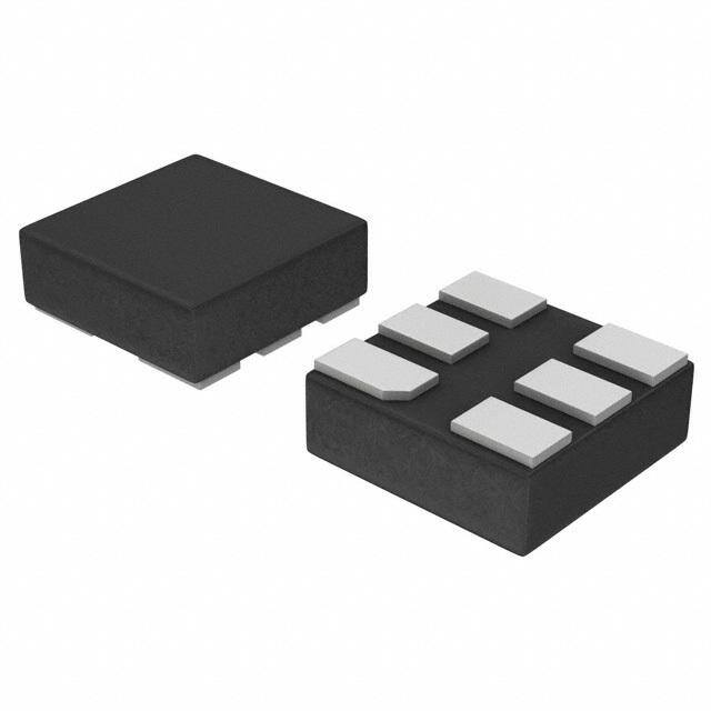
ICGOO电子元器件商城为您提供NLU1GT50CMX1TCG由ON Semiconductor设计生产,在icgoo商城现货销售,并且可以通过原厂、代理商等渠道进行代购。 NLU1GT50CMX1TCG价格参考。ON SemiconductorNLU1GT50CMX1TCG封装/规格:逻辑 - 缓冲器,驱动器,接收器,收发器, Buffer, Non-Inverting 1 Element 1 Bit per Element Push-Pull Output 6-ULLGA (1x1)。您可以下载NLU1GT50CMX1TCG参考资料、Datasheet数据手册功能说明书,资料中有NLU1GT50CMX1TCG 详细功能的应用电路图电压和使用方法及教程。
ON Semiconductor(安森美半导体)的NLU1GT50CMX1TCG是一款逻辑缓冲器、驱动器、接收器和收发器类别的器件。以下是其主要应用场景:

 1. 数据通信与接口
   - NLU1GT50CMX1TCG适用于高速数据传输场景,例如在计算机、网络设备或工业控制系统中实现信号的放大和整形。
   - 它可以作为接口芯片,用于连接不同逻辑电平的系统,确保信号兼容性和完整性。

 2. 工业自动化
   - 在工业自动化领域,该器件可用于传感器信号处理、PLC(可编程逻辑控制器)输入/输出模块以及现场总线通信。
   - 其高可靠性设计使其能够在恶劣环境下稳定工作,如高温、振动或电磁干扰强的环境。

 3. 汽车电子
   - 该芯片适合应用于车载信息娱乐系统、车身控制模块(BCM)及ADAS(高级驾驶辅助系统)中的信号传输。
   - 它能够支持CAN、LIN或其他汽车总线协议,提供可靠的信号驱动能力。

 4. 消费电子
   - 在家用电器或消费电子产品中,NLU1GT50CMX1TCG可用于音频/视频设备的信号切换、显示面板的时序控制以及遥控器的信号处理。
   - 其低功耗特性有助于延长电池寿命并减少发热。

 5. 医疗设备
   - 该器件可用于医疗监测设备中的信号调理电路,例如心率监测仪、血压计或超声波设备。
   - 它能确保信号的精确传递,同时满足医疗级产品的严格要求。

 6. 航空航天与国防
   - 在需要高可靠性和抗辐射性能的应用中,如卫星通信、雷达系统或导弹制导系统,NLU1GT50CMX1TCG可以提供稳定的信号驱动和缓冲功能。

 总结
NLU1GT50CMX1TCG凭借其高性能、低功耗和高可靠性,广泛应用于数据通信、工业自动化、汽车电子、消费电子、医疗设备以及航空航天等领域。它能够有效解决信号完整性问题,为各种复杂系统提供强大的逻辑支持。
| 参数 | 数值 |
| 产品目录 | 集成电路 (IC)半导体 |
| 描述 | IC BUFFER TTL NON-INVERT 6ULLGA缓冲器和线路驱动器 NON INVRT BUFF TTL |
| 产品分类 | |
| 品牌 | ON Semiconductor |
| 产品手册 | |
| 产品图片 |
|
| rohs | 符合RoHS无铅 / 符合限制有害物质指令(RoHS)规范要求 |
| 产品系列 | 逻辑集成电路,缓冲器和线路驱动器,ON Semiconductor NLU1GT50CMX1TCG- |
| 数据手册 | |
| 产品型号 | NLU1GT50CMX1TCG |
| 产品种类 | 缓冲器和线路驱动器 |
| 传播延迟时间 | 19.5 ns at 2.3 V to 2.7 V, 13.5 ns at 3 V to 3.6 V, 7.7 ns at 4.5 V to 5.5 V |
| 低电平输出电流 | 8 mA |
| 供应商器件封装 | 6-ULLGA(1x1) |
| 元件数 | 1 |
| 包装 | 带卷 (TR) |
| 商标 | ON Semiconductor |
| 安装类型 | 表面贴装 |
| 安装风格 | SMD/SMT |
| 封装 | Reel |
| 封装/外壳 | 6-XFLGA |
| 封装/箱体 | ULLGA-6 |
| 工作温度 | -55°C ~ 125°C |
| 工厂包装数量 | 3000 |
| 最大工作温度 | + 125 C |
| 最小工作温度 | - 55 C |
| 极性 | Non-Inverting |
| 标准包装 | 3,000 |
| 每元件位数 | 1 |
| 每芯片的通道数量 | 1 |
| 电压-电源 | 1.65 V ~ 5.5 V |
| 电流-输出高,低 | 8mA,8mA |
| 电源电压-最大 | 5.5 V |
| 电源电压-最小 | 1.65 V |
| 系列 | NLU1GT50 |
| 输入线路数量 | 1 |
| 输出线路数量 | 1 |
| 逻辑类型 | CMOS |
| 高电平输出电流 | - 8 mA |


- 商务部:美国ITC正式对集成电路等产品启动337调查
- 曝三星4nm工艺存在良率问题 高通将骁龙8 Gen1或转产台积电
- 太阳诱电将投资9.5亿元在常州建新厂生产MLCC 预计2023年完工
- 英特尔发布欧洲新工厂建设计划 深化IDM 2.0 战略
- 台积电先进制程称霸业界 有大客户加持明年业绩稳了
- 达到5530亿美元!SIA预计今年全球半导体销售额将创下新高
- 英特尔拟将自动驾驶子公司Mobileye上市 估值或超500亿美元
- 三星加码芯片和SET,合并消费电子和移动部门,撤换高东真等 CEO
- 三星电子宣布重大人事变动 还合并消费电子和移动部门
- 海关总署:前11个月进口集成电路产品价值2.52万亿元 增长14.8%


PDF Datasheet 数据手册内容提取
NLU1GT50 Single Buffer, Non-Inverting, TTL Level TTL−Compatible Inputs The NLU1GT50 MiniGate(cid:2) is an advanced CMOS high−speed www.onsemi.com non−inverting buffer in ultra−small footprint. The device input is compatible with TTL−type input thresholds and MARKING the output has a full 5.0 V CMOS level output swing. DIAGRAMS The NLU1GT50 input and output structures provide protection when voltages up to 7.0 V are applied, regardless of the supply UDFN6 voltage. MU SUFFIX LM CASE 517AA 1 Features • Designed for 1.65 to 5.5 V V Operation CC • ULLGA6 High Speed: tPD = 3.5 ns (Typ) @ VCC = 5.0 V 1.0 x 1.0 LM • Low Power Dissipation: I = 1 (cid:2)A (Max) at T = 25°C CASE 613AD CC A 1 • TTL−Compatible Input: V = 0.8 V; V = 2.0 V, V = 5.0 V IL IH CC • CMOS−Compatible Output: ULLGA6 V > 0.8 V ; V < 0.1 V @ Load OH CC OL CC 1.45 x 1.0 LM • Power Down Protection Provided on inputs CASE 613AF • 1 Balanced Propagation Delays • Ultra−Small Packages • UDFN6 These are Pb−Free Devices 1.0 x 1.0 V M CASE 517BX 1 NC 1 6 VCC UDFN6 1.45 x 1.0 R M CASE 517AQ 1 IN A 2 5 NC L = Device Marking M = Date Code GND 3 4 OUT Y ORDERING INFORMATION Figure 1. Pinout (Top View) See detailed ordering and shipping information on page 4 of this data sheet. IN A 1 OUT Y Figure 2. Logic Symbol PIN ASSIGNMENT 1 NC 2 IN A FUNCTION TABLE 3 GND A Y 4 OUT Y L L 5 NC H H 6 VCC © Semiconductor Components Industries, LLC, 2016 1 Publication Order Number: June, 2016 − Rev. 5 NLU1GT50/D
NLU1GT50 MAXIMUM RATINGS Symbol Parameter Value Unit VCC DC Supply Voltage −0.5 to +7.0 V VIN DC Input Voltage −0.5 to +7.0 V VOUT DC Output Voltage −0.5 to +7.0 V IIK DC Input Diode Current VIN < GND −20 mA IOK DC Output Diode Current VOUT < GND ±20 mA IO DC Output Source/Sink Current ±12.5 mA ICC DC Supply Current Per Supply Pin ±25 mA IGND DC Ground Current per Ground Pin ±25 mA TSTG Storage Temperature Range −65 to +150 °C TL Lead Temperature, 1 mm from Case for 10 Seconds 260 °C TJ Junction Temperature Under Bias 150 °C MSL Moisture Sensitivity Level 1 FR Flammability Rating Oxygen Index: 28 to 34 UL 94 V−0 @ 0.125 in VESD ESD Withstand Voltage Human Body Model (Note 2) > 2000 V Machine Model (Note 3) > 200 Charged Device Model (Note 4) N/A ILATCHUP1 Latchup Performance Above VCC and Below GND at 125 °C (Note 5) ±500 mA Stresses exceeding those listed in the Maximum Ratings table may damage the device. If any of these limits are exceeded, device functionality should not be assumed, damage may occur and reliability may be affected. 1. Measured with minimum pad spacing on an FR4 board, using 10 mm−by−1 inch, 2 ounce copper trace no air flow. 2. Tested to EIA / JESD22−A114−A. 3. Tested to EIA / JESD22−A115−A. 4. Tested to JESD22−C101−A. 5. Tested to EIA / JESD78. RECOMMENDED OPERATING CONDITIONS Symbol Parameter Min Max Unit VCC Positive DC Supply Voltage 1.65 5.5 V VIN Digital Input Voltage 0 5.5 V VOUT Output Voltage 0 5.5 V TA Operating Free−Air Temperature −55 +125 °C (cid:3)t/(cid:3)V Input Transition Rise or Fall Rate VCC = 3.3 V ± 0.3 V 0 100 ns/V VCC = 5.0 V ± 0.5 V 0 20 www.onsemi.com 2
NLU1GT50 DC ELECTRICAL CHARACTERISTICS TA = −55(cid:2)C to TA = 25 (cid:2)C TA = +85(cid:2)C +125(cid:2)C Symbol Parameter Conditions VCC (V) Min Typ Max Min Max Min Max Unit VIH Low−Level 1.65 to 0.50 x 0.50 x V Input 2.29 VCC VCC Voltage 2.3 to 2.99 0.45 x 0.45 x VCC VCC 3.0 1.4 1.4 4.5 to 5.5 2.0 2.0 VIL Low−Level 1.65 to 0.10 x 0.10 x 0.10 x V Input 2.29 VCC VCC VCC Voltage 2.3 to 2.99 0.15 x 0.15 x 0.15 x VCC VCC VCC 3.0 0.53 0.53 0.53 4.5 to 5.5 0.8 0.8 0.8 VOH High−Level VIN = VIH or VIL 1.65 to VCC– VCC– VCC– V Output 2.99 0.1 0.1 0.1 Voltage IOH = −50 (cid:2)A 3.0 2.9 3.0 2.9 2.9 4.5 4.4 4.5 4.4 4.4 VIN = VIH or VIL IOH = −4 mA 3.0 2.58 2.48 2.34 IOH = −8 mA 4.5 3.94 3.80 3.66 VOL Low−Level VIN = VIH or VIL 1.65 to 0 0.1 0.1 0.1 V Output IOL = 50 (cid:2)A 2.99 Voltage 3.0 0 0.1 0.1 0.1 4.5 0 0.1 0.1 0.1 VIN = VIH or VIL IOL = 4 mA 3.0 0.36 0.44 0.52 IOL = 8 mA 4.5 0.36 0.44 0.52 IIN Input 0 = VIN = 5.5 V 0 to 5.5 ±0.1 ±1.0 ±1.0 (cid:2)A Leakage Current ICC Quiescent VIN = 5.5 V or 5.5 1.0 20 40 (cid:2)A Supply GND Current ICCT Quiescent VIN = 3.4 V 5.5 1.35 1.50 1.65 mA Supply Current IOPD Output VOUT = 5.5 V 0.0 0.5 5.0 10 (cid:2)A Leakage Current www.onsemi.com 3
NLU1GT50 AC ELECTRICAL CHARACTERISTICS (Input tr = tf = 3.0 n) TA = −55(cid:2)C Test TA = 25 (cid:2)C TA = +85(cid:2)C to +125(cid:2)C Symbol Parameter VCC (V) Condition Min Typ Max Min Max Min Max Unit tPLH, Propagation Delay, 1.65 to 1.95 CL = 15 pF 16.6 18.0 22.0 ns tPHL Input A to Output Y 2.3 to 2.7 CL = 15 pF 13.3 14.5 17.5 CL = 50 pF 19.5 22.0 25.5 3.0 to 3.6 CL = 15 pF 4.5 10.0 11.0 13.0 CL = 50 pF 6.3 13.5 15.0 17.5 4.5 to 5.5 CL = 15 pF 3.5 6.7 7.5 8.5 CL = 50 pF 4.3 7.7 8.5 9.5 CIN Input Capacitance 5 10 10 10.0 pF CPD Power Dissipation 5.0 12 pF Capacitance (Note 6) 6. CPD is defined as the value of the internal equivalent capacitance which is calculated from the dynamic operating current consumption without load. Average operating current can be obtained by the equation ICC(OPR) = CPD • VCC • fin + ICC. CPD is used to determine the no−load dynamic power consumption: PD = CPD • VCC2 • fin + ICC • VCC. TEST POINT A VCC OUTPUT 50% DEVICE GND UNDER tPLH tPHL TEST CL* VOH Y 50% VCC VOL *Includes all probe and jig capacitance Figure 3. Switching Waveforms Figure 4. Test Circuit ORDERING INFORMATION Device Package Shipping† NLU1GT50MUTCG UDFN6, 1.2 x 1.0, 0.4P 3000 / Tape & Reel (Pb−Free) NLU1GT50AMX1TCG ULLGA6, 1.45 x 1.0, 0.5P 3000 / Tape & Reel (Pb−Free) NLU1GT50CMX1TCG ULLGA6, 1.0 x 1.0, 0.35P 3000 / Tape & Reel (Pb−Free) NLU1GT50AMUTCG UDFN6, 1.45 x 1.0, 0.5P 3000 / Tape & Reel (Pb−Free) NLU1GT50CMUTCG UDFN6, 1.0 x 1.0, 0.35P 3000 / Tape & Reel (Pb−Free) †For information on tape and reel specifications, including part orientation and tape sizes, please refer to our Tape and Reel Packaging Specifications Brochure, BRD8011/D. www.onsemi.com 4
NLU1GT50 PACKAGE DIMENSIONS UDFN6 1.45x1.0, 0.5P CASE 517AQ ISSUE O D A L L NOTES: B 1. DIMENSIONING AND TOLERANCING PER ASME Y14.5M, 1994. L1 2. CONTROLLING DIMENSION: MILLIMETERS. 3. DIMENSION b APPLIES TO PLATED TERMINAL AND IS MEASURED BETWEEN 0.15 AND DETAIL A 0.30 mm FROM THE TERMINAL TIP. ÉÉÉ PIN ONE E OPTIONAL REFERENCE CONSTRUCTIONS MILLIMETERS ÉÉÉ DIM MIN MAX A 0.45 0.55 0.10 C A1 0.00 0.05 EXPOSED Cu MOLD CMPD A2 0.07 REF TOP VIEW ÉÉÉÉ b 0.20 0.30 0.10 C D 1.45 BSC ÉÉ E 1.00 BSC DETAIL B e 0.50 BSC DETAIL B L 0.30 0.40 0.05 C OPTIONAL L1 −−− 0.15 A CONSTRUCTIONS MOUNTING FOOTPRINT 6X 0.05 C A1 SIDE VIEW A2 C SPELAATNIENG 06X.30 PACKAGE OUTLINE e 6XL 1.24 1 3 DETAIL A 6X 1 0.53 0.50 PITCH 6 4 6Xb DIMENSIONS: MILLIMETERS 0.10 C A B *For additional information on our Pb−Free strategy and soldering details, please download the ON Semiconductor Soldering and BOTTOM VIEW 0.05 C NOTE 3 Mounting Techniques Reference Manual, SOLDERRM/D. www.onsemi.com 5
NLU1GT50 PACKAGE DIMENSIONS UDFN6 1.0x1.0, 0.35P CASE 517BX ISSUE O D A B NOTES: 1. DIMENSIONING AND TOLERANCING PER ASME Y14.5M, 1994. 2. CONTROLLING DIMENSION: MILLIMETERS. 3. DIMENSION b APPLIES TO PLATED PIN ONE ÉÉÉ TERMINAL AND IS MEASURED BETWEEN REFERENCE E 0.15 AND 0.20 MM FROM TERMINAL TIP. 4. PACKAGE DIMENSIONS EXCLUSIVE OF ÉÉÉ BURRS AND MOLD FLASH. 2X 0.10 C ÉÉÉ MILLIMETERS DIM MIN MAX 2X 0.10 C A 0.45 0.55 TOP VIEW A1 0.00 0.05 A3 0.13 REF b 0.12 0.22 0.05 C A3 D 1.00 BSC E 1.00 BSC A e 0.35 BSC L 0.25 0.35 L1 0.30 0.40 0.05 C SIDE VIEW A1 C SEATING RECOMMENDED PLANE SOLDERING FOOTPRINT* e 05.4X8 6X 5XL 0.22 1 3 L1 1.18 6 4 6Xb 1 0.35 0.53 0.10 M C A B PKG PITCH OUTLINE BOTTOM VIEW 0.05 M C NOTE 3 DIMENSIONS: MILLIMETERS *For additional information on our Pb−Free strategy and soldering details, please download the ON Semiconductor Soldering and Mounting Techniques Reference Manual, SOLDERRM/D. www.onsemi.com 6
NLU1GT50 PACKAGE DIMENSIONS UDFN6, 1.2x1.0, 0.4P CASE 517AA ISSUE D EDGE OF PACKAGE D A NOTES: 1. DIMENSIONING AND TOLERANCING PER B ASME Y14.5M, 1994. 2. CONTROLLING DIMENSION: MILLIMETERS. 3. DIMENSION b APPLIES TO PLATED TERMINAL L1 AND IS MEASURED BETWEEN 0.25 AND 0.30 mm FROM TERMINAL. 4. COPLANARITY APPLIES TO THE EXPOSED REFEPRINE ONCNEE ÉÉ E DETAIL A PAD AS WELL AS THE TERMINALS. Bottom View MILLIMETERS 2X ÉÉ (Optional) DIM MIN MAX 0.10 C A 0.45 0.55 A1 0.00 0.05 TOP VIEW EXPOSED Cu MOLD CMPD A3 0.127 REF 2X ÉÉÉ b 0.15 0.25 0.10 C D 1.20 BSC ÉÉÉÉÉÉ A3 E 1.00 BSC e 0.40 BSC L 0.30 0.40 0.10 C (A3) A1 DETAIL B LL12 00..0400 00..1550 Side View A (Optional) 10X 0.08 C SIDE VIEW SPELAATNIENG MOUNTING FOOTPRINT* 6X A1 C 0.42 6X 0.22 5XL 1 3 L2 6Xb 0.10 C A B 6 4 0.40 1.07 PITCH 0.05 C e NOTE 3 DIMENSIONS: MILLIMETERS BOTTOM VIEW *For additional information on our Pb−Free strategy and soldering details, please download the ON Semiconductor Soldering and Mounting Techniques Reference Manual, SOLDERRM/D. www.onsemi.com 7
NLU1GT50 PACKAGE DIMENSIONS ULLGA6 1.0x1.0, 0.35P CASE 613AD ISSUE A D A NOTES: 1. DIMENSIONING AND TOLERANCING PER B ASME Y14.5M, 1994. 2. CONTROLLING DIMENSION: MILLIMETERS. 3. DIMENSION b APPLIES TO PLATED TERMINAL AND IS MEASURED BETWEEN 0.15 AND 0.30 mm FROM THE TERMINAL TIP. 4. A MAXIMUM OF 0.05 PULL BACK OF THE PIN ONE ÉÉ E PLATED TERMINAL FROM THE EDGE OF THE REFERENCE PACKAGE IS ALLOWED. ÉÉ MILLIMETERS 0.10 C DIM MIN MAX A −−− 0.40 TOP VIEW A1 0.00 0.05 0.10 C b 0.12 0.22 D 1.00 BSC E 1.00 BSC 0.05 C e 0.35 BSC L 0.25 0.35 L1 0.30 0.40 A 6X 0.05 C SIDE VIEW SPELAATNIENG SMOOLUDNETRIMNGAS FKO DOETFPIRNIENDT* A1 C 05.4X8 6X 0.22 e 5XL NOTE 4 1 3 1.18 L1 1 0.35 0.53 PKG PITCH 6 4 OUTLINE 6Xb DIMENSIONS: MILLIMETERS 0.10 C A B *For additional information on our Pb−Free strategy and soldering BOTTOM VIEW 0.05 C NOTE 3 details, please download the ON Semiconductor Soldering and Mounting Techniques Reference Manual, SOLDERRM/D. www.onsemi.com 8
NLU1GT50 PACKAGE DIMENSIONS ULLGA6 1.45x1.0, 0.5P CASE 613AF ISSUE A NOTES: D A 1. DIMENSIONING AND TOLERANCING PER ASME Y14.5M, 1994. B 2. CONTROLLING DIMENSION: MILLIMETERS. 3. DIMENSION b APPLIES TO PLATED TERMINAL AND IS MEASURED BETWEEN 0.15 AND 0.30 mm FROM THE TERMINAL TIP. 4. A MAXIMUM OF 0.05 PULL BACK OF THE ÉÉÉ PLATED TERMINAL FROM THE EDGE OF THE PIN ONE E PACKAGE IS ALLOWED. REFERENCE ÉÉÉ MILLIMETERS DIM MIN MAX 0.10 C A −−− 0.40 A1 0.00 0.05 TOP VIEW b 0.15 0.25 0.10 C D 1.45 BSC E 1.00 BSC e 0.50 BSC 0.05 C L 0.25 0.35 L1 0.30 0.40 A MOUNTING FOOTPRINT 6X 0.05 C SIDE VIEW SPELAATNIENG SOLDERMASK DEFINED* 5X A1 C 0.49 6X 0.30 e 5XL NOTE 4 1 3 1.24 L1 1 0.53 PKG 0.50 6 4 OUTLINE PITCH 6Xb DIMENSIONS: MILLIMETERS 0.10 C A B *For additional information on our Pb−Free strategy and soldering BOTTOM VIEW 0.05 C NOTE 3 details, please download the ON Semiconductor Soldering and Mounting Techniques Reference Manual, SOLDERRM/D. MiniGate is a trademark of Semiconductor Components Industries, LLC (SCILLC). ON Semiconductor and are trademarks of Semiconductor Components Industries, LLC dba ON Semiconductor or its subsidiaries in the United States and/or other countries. ON Semiconductor owns the rights to a number of patents, trademarks, copyrights, trade secrets, and other intellectual property. A listing of ON Semiconductor’s product/patent coverage may be accessed at www.onsemi.com/site/pdf/Patent−Marking.pdf. ON Semiconductor reserves the right to make changes without further notice to any products herein. ON Semiconductor makes no warranty, representation or guarantee regarding the suitability of its products for any particular purpose, nor does ON Semiconductor assume any liability arising out of the application or use of any product or circuit, and specifically disclaims any and all liability, including without limitation special, consequential or incidental damages. Buyer is responsible for its products and applications using ON Semiconductor products, including compliance with all laws, regulations and safety requirements or standards, regardless of any support or applications information provided by ON Semiconductor. “Typical” parameters which may be provided in ON Semiconductor data sheets and/or specifications can and do vary in different applications and actual performance may vary over time. All operating parameters, including “Typicals” must be validated for each customer application by customer’s technical experts. ON Semiconductor does not convey any license under its patent rights nor the rights of others. ON Semiconductor products are not designed, intended, or authorized for use as a critical component in life support systems or any FDA Class 3 medical devices or medical devices with a same or similar classification in a foreign jurisdiction or any devices intended for implantation in the human body. Should Buyer purchase or use ON Semiconductor products for any such unintended or unauthorized application, Buyer shall indemnify and hold ON Semiconductor and its officers, employees, subsidiaries, affiliates, and distributors harmless against all claims, costs, damages, and expenses, and reasonable attorney fees arising out of, directly or indirectly, any claim of personal injury or death associated with such unintended or unauthorized use, even if such claim alleges that ON Semiconductor was negligent regarding the design or manufacture of the part. ON Semiconductor is an Equal Opportunity/Affirmative Action Employer. This literature is subject to all applicable copyright laws and is not for resale in any manner. PUBLICATION ORDERING INFORMATION LITERATURE FULFILLMENT: N. American Technical Support: 800−282−9855 Toll Free ON Semiconductor Website: www.onsemi.com Literature Distribution Center for ON Semiconductor USA/Canada 19521 E. 32nd Pkwy, Aurora, Colorado 80011 USA Europe, Middle East and Africa Technical Support: Order Literature: http://www.onsemi.com/orderlit Phone: 303−675−2175 or 800−344−3860 Toll Free USA/Canada Phone: 421 33 790 2910 Fax: 303−675−2176 or 800−344−3867 Toll Free USA/Canada Japan Customer Focus Center For additional information, please contact your local Email: orderlit@onsemi.com Phone: 81−3−5817−1050 Sales Representative www.onsemi.com NLU1GT50/D 9