 Datasheet下载
- 型号: SN74HC573ADW
- 制造商: Texas Instruments
- 库位|库存: xxxx|xxxx
- 要求:
| 数量阶梯 | 香港交货 | 国内含税 |
| +xxxx | $xxxx | ¥xxxx |
查看当月历史价格
查看今年历史价格
SN74HC573ADW产品简介:
ICGOO电子元器件商城为您提供SN74HC573ADW由Texas Instruments设计生产,在icgoo商城现货销售,并且可以通过原厂、代理商等渠道进行代购。 SN74HC573ADW价格参考¥0.85-¥1.12。Texas InstrumentsSN74HC573ADW封装/规格:逻辑 - 锁销, D-Type Transparent Latch 1 Channel 8:8 IC Tri-State 20-SOIC。您可以下载SN74HC573ADW参考资料、Datasheet数据手册功能说明书,资料中有SN74HC573ADW 详细功能的应用电路图电压和使用方法及教程。
Texas Instruments(德州仪器)的SN74HC573ADW是一款8位透明锁存器,属于逻辑电路中的锁存器(Latch)类别。它广泛应用于需要数据暂存和信号传输控制的场景中。以下是其主要应用场景:

1. 微处理器与外设接口:在微处理器系统中,SN74HC573ADW可以用于扩展并行端口或作为缓冲器,将来自微处理器的数据暂时存储起来,然后在适当的时机输出到外部设备。这种应用常见于工业控制系统、嵌入式系统等。

2. LED驱动与显示控制:对于多段LED显示器或多路LED阵列,该器件可以用作地址译码器或数据锁存器,确保每个LED能够在正确的时间点被点亮,避免闪烁或错误显示。

3. 通信协议转换:在一些串行到并行转换或者反之亦然的应用中,例如SPI、I2C总线与其他并行总线之间的桥接,SN74HC573ADW可以帮助同步数据流,提高系统的稳定性和可靠性。

4. 电机控制与驱动电路:在步进电机或其他类型电机的驱动电路中,这款锁存器能够协调多个输入信号,以精确控制电机的动作顺序和方向,特别是在多轴运动控制系统中尤为重要。

5. 音频处理与视频切换:在音频混音器或视频矩阵开关等设备里,它可以用来管理多个输入源的选择和输出分配,保证信号的准确传递而不受干扰。

6. 自动化测试设备(ATE):用于构建复杂的测试平台,通过编程设置不同的状态组合来进行各种功能测试,如集成电路测试仪、印刷电路板检测仪等。

总之,SN74HC573ADW凭借其高性能特性和广泛的兼容性,在众多领域都扮演着重要的角色,特别是在那些需要高效管理和传递数字信号的应用场合。
| 参数 | 数值 |
| 产品目录 | 集成电路 (IC)半导体 |
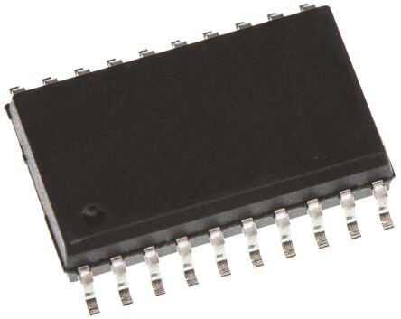
| 描述 | IC OCT D-TYPE LATCH 20-SOIC闭锁 Tri-St Octal D-Type |
| 产品分类 | |
| 品牌 | Texas Instruments |
| 产品手册 | |
| 产品图片 |
|
| rohs | 符合RoHS无铅 / 符合限制有害物质指令(RoHS)规范要求 |
| 产品系列 | 逻辑集成电路,闭锁,Texas Instruments SN74HC573ADW74HC |
| 数据手册 | |
| 产品型号 | SN74HC573ADW |
| 产品目录页面 | |
| 产品种类 | 闭锁 |
| 传播延迟时间 | 21 ns |
| 低电平输出电流 | 6 mA |
| 供应商器件封装 | 20-SOIC |
| 其它名称 | 296-1203-5 |
| 包装 | 管件 |
| 单位重量 | 500.700 mg |
| 商标 | Texas Instruments |
| 安装类型 | 表面贴装 |
| 安装风格 | SMD/SMT |
| 封装 | Tube |
| 封装/外壳 | 20-SOIC(0.295",7.50mm 宽) |
| 封装/箱体 | SOIC-20 |
| 工作温度 | -40°C ~ 85°C |
| 工厂包装数量 | 25 |
| 延迟时间-传播 | 23ns |
| 最大工作温度 | + 85 C |
| 最小工作温度 | - 40 C |
| 极性 | Non-Inverting |
| 标准包装 | 25 |
| 独立电路 | 1 |
| 电压-电源 | 2 V ~ 6 V |
| 电流-输出高,低 | 7.8mA,7.8mA |
| 电源电压-最大 | 6 V |
| 电源电压-最小 | 2 V |
| 电源电流 | 8 uA |
| 电路 | 8:8 |
| 电路数量 | 8 Circuit |
| 系列 | SN74HC573A |
| 输入线路数量 | 8 Line |
| 输出类型 | 三态 |
| 输出线路数量 | 8 Line |
| 逻辑类型 | D 型透明锁存器 |
| 逻辑系列 | 74HC |
| 高电平输出电流 | - 6 mA |


- 商务部:美国ITC正式对集成电路等产品启动337调查
- 曝三星4nm工艺存在良率问题 高通将骁龙8 Gen1或转产台积电
- 太阳诱电将投资9.5亿元在常州建新厂生产MLCC 预计2023年完工
- 英特尔发布欧洲新工厂建设计划 深化IDM 2.0 战略
- 台积电先进制程称霸业界 有大客户加持明年业绩稳了
- 达到5530亿美元!SIA预计今年全球半导体销售额将创下新高
- 英特尔拟将自动驾驶子公司Mobileye上市 估值或超500亿美元
- 三星加码芯片和SET,合并消费电子和移动部门,撤换高东真等 CEO
- 三星电子宣布重大人事变动 还合并消费电子和移动部门
- 海关总署:前11个月进口集成电路产品价值2.52万亿元 增长14.8%


PDF Datasheet 数据手册内容提取
Product Sample & Technical Tools & Support & Folder Buy Documents Software Community SN54HC573A,SN74HC573A SCLS147F–DECEMBER1982–REVISEDOCTOBER2016 SNx4HC573A Octal Transparent D-Type Latches With 3-State Outputs 1 Features 3 Description • WideOperatingVoltageRangefrom2Vto6V The SNx4HC573A devices are octal transparent 1 D-type latches that feature 3-state outputs designed • High-Current3-StateOutputsDriveBusLines specifically for driving highly capacitive or relatively Directlyupto15LSTTLLoads low-impedance loads. They are particularly suitable • LowPowerConsumption:80-µAMaximumI for implementing buffer registers, I/O ports, CC • Typicalt =21ns bidirectionalbusdrivers,andworkingregisters. pd • ±6-mAOutputDriveat5V While the latch-enable (LE) input is high, the Q outputs respond to the data (D) inputs. When LE is • LowInputCurrent:1µA(Maximum) low, the outputs are latched to retain the data that • Bus-StructuredPinout wassetup. 2 Applications DeviceInformation(1) • BufferRegisters PARTNUMBER PACKAGE BODYSIZE(NOM) • BidirectionalBusDrivers SN54HC573AJ CDIP(20) 26.92mm×6.92mm • WorkingRegisters SN54HC573AW CFP(20) 13.72mm×6.92mm SN54HC573AFK LCCC(20) 8.89mm×8.89mm SN74HC573AN PDIP(20) 25.40mm×6.35mm SN74HC573ADW SOIC(20) 12.80mm×7.50mm SN74HC573ADB SSOP(20) 7.20mm×5.30mm SN74HC573APW TSSOP(20) 5.00mm×4.40mm (1) For all available packages, see the orderable addendum at theendofthedatasheet. LogicDiagram(PositiveLogic) 1 OE 11 LE C1 19 2 1Q 1D 1D To Seven Other Channels Copyright © 2016,Texas Instruments Incorporated 1 An IMPORTANT NOTICE at the end of this data sheet addresses availability, warranty, changes, use in safety-critical applications, intellectualpropertymattersandotherimportantdisclaimers.PRODUCTIONDATA. On products compliant to MIL-PRF-38535, all parameters are testedunlessotherwisenoted.Onallotherproducts,production processingdoesnotnecessarilyincludetestingofallparameters.
SN54HC573A,SN74HC573A SCLS147F–DECEMBER1982–REVISEDOCTOBER2016 www.ti.com Table of Contents 1 Features.................................................................. 1 8.3 FeatureDescription.................................................10 2 Applications........................................................... 1 8.4 DeviceFunctionalModes........................................10 3 Description............................................................. 1 9 ApplicationandImplementation........................ 11 4 RevisionHistory..................................................... 2 9.1 ApplicationInformation............................................11 9.2 TypicalApplication..................................................11 5 PinConfigurationandFunctions......................... 3 10 PowerSupplyRecommendations..................... 12 6 Specifications......................................................... 4 11 Layout................................................................... 12 6.1 AbsoluteMaximumRatings......................................4 6.2 ESDRatings..............................................................4 11.1 LayoutGuidelines.................................................12 6.3 RecommendedOperatingConditions.......................4 11.2 LayoutExample....................................................12 6.4 ThermalInformation..................................................5 12 DeviceandDocumentationSupport................. 13 6.5 ElectricalCharacteristics...........................................5 12.1 DocumentationSupport........................................13 6.6 TimingRequirements................................................6 12.2 RelatedLinks........................................................13 6.7 SwitchingCharacteristics..........................................6 12.3 ReceivingNotificationofDocumentationUpdates13 6.8 TypicalCharacteristics..............................................8 12.4 CommunityResources..........................................13 7 ParameterMeasurementInformation..................9 12.5 Trademarks...........................................................13 12.6 ElectrostaticDischargeCaution............................13 8 DetailedDescription............................................ 10 12.7 Glossary................................................................13 8.1 Overview.................................................................10 13 Mechanical,Packaging,andOrderable 8.2 FunctionalBlockDiagram.......................................10 Information........................................................... 13 4 Revision History NOTE:Pagenumbersforpreviousrevisionsmaydifferfrompagenumbersinthecurrentversion. ChangesfromRevisionE(September2003)toRevisionF Page • AddedESDRatingstable,FeatureDescriptionsection,DeviceFunctionalModes,ApplicationandImplementation section,PowerSupplyRecommendationssection,Layoutsection,DeviceandDocumentationSupportsection,and Mechanical,Packaging,andOrderableInformationsection.................................................................................................. 1 • DeletedOrderingInformationtable;seePOAattheendofthedatasheet........................................................................... 1 • ChangedPackagethermalimpedance,R ,valuesfrom70to92.5(DB),from58to78.3(DW),from69to49.1 θJA (N),andfrom83to101.1(PW).............................................................................................................................................. 5 2 SubmitDocumentationFeedback Copyright©1982–2016,TexasInstrumentsIncorporated ProductFolderLinks:SN54HC573A SN74HC573A
SN54HC573A,SN74HC573A www.ti.com SCLS147F–DECEMBER1982–REVISEDOCTOBER2016 5 Pin Configuration and Functions DB,DW,J,N,PW,orWPackages FKPackage 20-PinSSOP,SOIC,CDIP,PDIP,TSSOP,orCFP 20-PinLCCC TopView TopView C OE 1 20 VCC 2D 1D OE VC 1Q 1D 2 19 1Q 2D 3 18 2Q 3 2 1 0 9 2 1 3D 4 17 3Q 3D 4 18 2Q 4D 5 16 4Q 4D 5 17 3Q 5D 6 15 5Q 5D 6 16 4Q 6D 7 14 6Q 7D 8 13 7Q 6D 7 15 5Q 8D 9 12 8Q 7D 8 14 6Q GND 10 11 LE 0 1 2 3 9 1 1 1 1 Not to scale Not to scale D D E Q Q 8 N L 8 7 G PinFunctions PIN I/O DESCRIPTION NO. NAME 1 OE I Outputenable 2 1D I 1Dinput 3 2D I 2Dinput 4 3D I 3Dinput 5 4D I 4Dinput 6 5D I 5Dinput 7 6D I 6Dinput 8 7D I 7Dinput 9 8D I 8Dinput 10 GND — Ground 11 LE I Latchenableinput 12 8Q O 8Qoutput 13 7Q O 7Qoutput 14 6Q O 6Qoutput 15 5Q O 5Qoutput 16 4Q O 4Qoutput 17 3Q O 3Qoutput 18 2Q O 2Qoutput 19 1Q O 1Qoutput 20 V — Powerpin CC Copyright©1982–2016,TexasInstrumentsIncorporated SubmitDocumentationFeedback 3 ProductFolderLinks:SN54HC573A SN74HC573A
SN54HC573A,SN74HC573A SCLS147F–DECEMBER1982–REVISEDOCTOBER2016 www.ti.com 6 Specifications 6.1 Absolute Maximum Ratings overoperatingfree-airtemperaturerange(unlessotherwisenoted)(1) MIN MAX UNIT V Supplyvoltage –0.5 7 V CC I Inputclampcurrent(2) V <0orV >V ±20 mA IK I I CC I Outputclampcurrent(2) V <0orV >V ±20 mA OK O O CC I Continuousoutputcurrent V =0toV ±35 mA O O CC ContinuouscurrentthroughV orGND ±70 mA CC T Junctiontemperature 150 °C J T Storagetemperature –65 150 °C stg (1) StressesbeyondthoselistedunderAbsoluteMaximumRatingsmaycausepermanentdamagetothedevice.Thesearestressratings only,whichdonotimplyfunctionaloperationofthedeviceattheseoranyotherconditionsbeyondthoseindicatedunderRecommended OperatingConditions.Exposuretoabsolute-maximum-ratedconditionsforextendedperiodsmayaffectdevicereliability. (2) Theinputandoutputvoltageratingsmaybeexceedediftheinputandoutputcurrentratingsareobserved. 6.2 ESD Ratings VALUE UNIT Human-bodymodel(HBM),perANSI/ESDA/JEDECJS-001(1) ±3500 V Electrostaticdischarge V (ESD) Charged-devicemodel(CDM),perJEDECspecificationJESD22-C101(2) ±1000 (1) JEDECdocumentJEP155statesthat500-VHBMallowssafemanufacturingwithastandardESDcontrolprocess. (2) JEDECdocumentJEP157statesthat250-VCDMallowssafemanufacturingwithastandardESDcontrolprocess. 6.3 Recommended Operating Conditions overoperatingfree-airtemperaturerange(unlessotherwisenoted)(1) MIN NOM MAX UNIT V Supplyvoltage 2 5 6 V CC V =2V 1.5 CC V High-levelinputvoltage V =4.5V 3.15 V IH CC V =6V 4.2 CC V =2V 0.5 CC V Low-levelinputvoltage V =4.5V 1.35 V IL CC V =6V 1.8 CC V Inputvoltage 0 V V I CC V Outputvoltage 0 V V O CC V =2V 1000 CC t Inputtransition(riseandfall)time V =4.5V 500 ns t CC V =6V 400 CC SN54HC573A –55 125 T Operatingfree-airtemperature °C A SN74HC573A –40 85 (1) AllunusedinputsofthedevicemustbeheldatV orGNDtoensureproperdeviceoperation.SeetheImplicationsofSloworFloating CC CMOSInputsapplicationreport(SCBA004). 4 SubmitDocumentationFeedback Copyright©1982–2016,TexasInstrumentsIncorporated ProductFolderLinks:SN54HC573A SN74HC573A
SN54HC573A,SN74HC573A www.ti.com SCLS147F–DECEMBER1982–REVISEDOCTOBER2016 6.4 Thermal Information SN74HC573A THERMALMETRIC(1) DB DW N PW UNIT (SSOP) (SOIC) (PDIP) (TSSOP) 20PINS 20PINS 20PINS 20PINS R Junction-to-ambientthermalresistance 92.5 78.3 49.1 101.1 °C/W θJA R Junction-to-case(top)thermalresistance 53.9 42.8 35.9 35.9 °C/W θJC(top) R Junction-to-boardthermalresistance 47.6 46.2 30 52 °C/W θJB ψ Junction-to-topcharacterizationparameter 19.5 18 22.4 2.4 °C/W JT ψ Junction-to-boardcharacterizationparameter 47.2 45.7 29.9 51.5 °C/W JB (1) Formoreinformationabouttraditionalandnewthermalmetrics,seetheSemiconductorandICPackageThermalMetricsapplication report. 6.5 Electrical Characteristics overoperatingfree-airtemperaturerange(unlessotherwisenoted) PARAMETER TESTCONDITIONS MIN TYP MAX UNIT V =2V 1.9 1.998 CC I =–20µA V =4.5V 4.4 4.499 OH CC V =6V 5.9 5.999 CC T =25°C 3.98 4.3 A V V =V orV I =–6mA,V =4.5V SN54HC573A 3.7 V OH I IH IL OH CC SN74HC573A 3.84 T =25°C 5.48 5.8 A I =–7.8mA,V =6V SN54HC573A 5.2 OH CC SN74HC573A 5.34 V =2V 0.002 0.1 CC I =20µA V =4.5V 0.001 0.1 OL CC V =6V 0.001 0.1 CC T =25°C 0.17 0.26 A V V =V orV I =6mA,V =4.5V SN54HC573A 0.4 V OL I IH IL OL CC SN74HC573A 0.33 T =25°C 0.15 0.26 A I =7.8mA,V =6V SN54HC573A 0.4 OL CC SN74HC573A 0.33 T =25°C ±0.1 ±100 A I V =V or0,V =6V nA I I CC CC SNx4HC573A ±1000 T =25°C ±0.01 ±0.5 A I V =V or0,V =6V SN54HC573A ±10 µA OZ O CC CC SN74HC573A ±5 T =25°C 8 A I V =V or0,I =0,V =6V SN54HC573A 160 µA CC I CC O CC SN74HC573A 80 C V =2Vto6V 3 10 pF i CC Powerdissipation C capacitance T =25°C,noload 50 pF pd A perlatch Copyright©1982–2016,TexasInstrumentsIncorporated SubmitDocumentationFeedback 5 ProductFolderLinks:SN54HC573A SN74HC573A
SN54HC573A,SN74HC573A SCLS147F–DECEMBER1982–REVISEDOCTOBER2016 www.ti.com 6.6 Timing Requirements overoperatingfree-airtemperaturerange(unlessotherwisenoted) MIN NOM MAX UNIT T =25°C 80 A V =2V SN54HC573A 120 CC SN74HC573A 100 T =25°C 16 A t Pulseduration,LEhigh V =4.5V SN54HC573A 24 ns w CC SN74HC573A 20 T =25°C 14 A V =6V SN54HC573A 20 CC SN74HC573A 17 T =25°C 50 A V =2V SN54HC573A 75 CC SN74HC573A 63 T =25°C 10 A t Setuptime,databeforeLE↓ V =4.5V SN54HC573A 15 ns su CC SN74HC573A 13 T =25°C 9 A V =6V SN54HC573A 13 CC SN74HC573A 11 T =25°C 20 A V =2V CC SNx4HC573A 24 t Holdtime,dataafterLE↓ ns h V =4.5V 5 CC V =6V 5 CC 6.7 Switching Characteristics overoperatingfree-airtemperaturerange(unlessotherwisenoted;seeFigure2) PARAMETER TESTCONDITIONS MIN TYP MAX UNIT T =25°C 77 175 A V =2V SN54HC573A 265 CC SN74HC573A 220 T =25°C 26 35 A C =50pF,fromD(input) L V =4.5V SN54HC573A 53 toQ(output) CC SN74HC573A 44 T =25°C 23 30 A V =6V SN54HC573A 45 CC SN74HC573A 38 t ns pd T =25°C 87 175 A V =2V SN54HC573A 265 CC SN74HC573A 220 T =25°C 27 35 A C =50pF,fromLE(input) L V =4.5V SN54HC573A 53 toanyQ(output) CC SN74HC573A 44 T =25°C 23 30 A V =6V SN54HC573A 45 CC SN74HC573A 38 6 SubmitDocumentationFeedback Copyright©1982–2016,TexasInstrumentsIncorporated ProductFolderLinks:SN54HC573A SN74HC573A
SN54HC573A,SN74HC573A www.ti.com SCLS147F–DECEMBER1982–REVISEDOCTOBER2016 Switching Characteristics (continued) overoperatingfree-airtemperaturerange(unlessotherwisenoted;seeFigure2) PARAMETER TESTCONDITIONS MIN TYP MAX UNIT T =25°C 68 150 A V =2V SN54HC573A 225 CC SN74HC573A 190 T =25°C 24 30 A C =50pF,fromOE(input) t L V =4.5V SN54HC573A 45 ns en toanyQ(output) CC SN74HC573A 38 T =25°C 21 26 A V =6V SN54HC573A 38 CC SN74HC573A 32 T =25°C 47 150 A V =2V SN54HC573A 225 CC SN74HC573A 190 T =25°C 23 30 A C =50pF,fromOE(input) t L V =4.5V SN54HC573A 45 ns dis toanyQ(output) CC SN74HC573A 38 T =25°C 21 26 A V =6V SN54HC573A 38 CC SN74HC573A 32 T =25°C 28 60 A V =2V SN54HC573A 90 CC SN74HC573A 75 T =25°C 8 12 A t C =50pFtoanyQ(output) V =4.5V SN54HC573A 18 ns t L CC SN74HC573A 15 T =25°C 6 10 A V =6V SN54HC573A 15 CC SN74HC573A 13 T =25°C 95 200 A V =2V SN54HC573A 300 CC SN74HC573A 250 T =25°C 33 40 A C =150pF,fromD(input) L V =4.5V SN54HC573A 60 toQ(output) CC SN74HC573A 50 T =25°C 21 34 A V =6V SN54HC573A 51 CC SN74HC573A 43 t ns pd T =25°C 103 225 A V =2V SN54HC573A 335 CC SN74HC573A 285 T =25°C 33 45 A C =150pF,fromLE(input)to L V =4.5V SN54HC573A 67 anyQ(output) CC SN74HC573A 57 T =25°C 29 40 A V =6V SN54HC573A 60 CC SN74HC573A 50 Copyright©1982–2016,TexasInstrumentsIncorporated SubmitDocumentationFeedback 7 ProductFolderLinks:SN54HC573A SN74HC573A
SN54HC573A,SN74HC573A SCLS147F–DECEMBER1982–REVISEDOCTOBER2016 www.ti.com Switching Characteristics (continued) overoperatingfree-airtemperaturerange(unlessotherwisenoted;seeFigure2) PARAMETER TESTCONDITIONS MIN TYP MAX UNIT T =25°C 85 200 A V =2V SN54HC573A 300 CC SN74HC573A 250 T =25°C 29 40 A C =150pF,fromOE(input) t L V =4.5V SN54HC573A 60 ns en toanyQ(output) CC SN74HC573A 50 T =25°C 26 34 A V =6V SN54HC573A 51 CC SN74HC573A 43 T =25°C 60 210 A V =2V SN54HC573A 315 CC SN74HC573A 265 T =25°C 17 42 A t C =150pFtoanyQ(output) V =4.5V SN54HC573A 63 ns t L CC SN74HC573A 53 T =25°C 14 36 A V =6V SN54HC573A 53 CC SN74HC573A 45 6.8 Typical Characteristics 250 CL 50pF 225 CL 150pF 200 175 s) x(n 150 a M D 125 P T 100 75 50 25 2 2.5 3 3.5 4 4.5 5 5.5 6 Vcc D001 Figure1.MaximumPropagationDelayCurves 8 SubmitDocumentationFeedback Copyright©1982–2016,TexasInstrumentsIncorporated ProductFolderLinks:SN54HC573A SN74HC573A
SN54HC573A,SN74HC573A www.ti.com SCLS147F–DECEMBER1982–REVISEDOCTOBER2016 7 Parameter Measurement Information VCC PARAMETER RL CL S1 S2 S1 tPZH 50 pF Open Closed Test ten 1 kΩ or From Output Point RL tPZL 150 pF Closed Open UnderTest tPHZ Open Closed CL tdis 1 kΩ 50 pF (see NoteA) S2 tPLZ Closed Open 50 pF tpdor tt −− or Open Open 150 pF LOAD CIRCUIT VCC Reference 50% Input High-Level VCC 0 V 50% 50% Pulse tsu th 0 V tw Data 90% 90% VCC 50% 50% VCC Input 10% 10% 0 V Low-Level 50% 50% Pulse tr tf 0 V VOLTAGEWAVEFORMS VOLTAGEWAVEFORMS PULSEDURATIONS SETUPANDHOLDANDINPUTRISEANDFALLTIMES VCC Output Input 50% 50% Control VCC 0 V (Low-Level 50% 50% tPLH tPHL Enabling) 0 V In-Phase VOH tPZL tPLZ Output 50% 90% 90% 50% Output ≈VCC ≈VCC 10% 10%VOL Waveform 1 50% tr tf (See Note B) 10% VOL tPHL tPLH VOH tPZH tPHZ 90% 90% Out-of- 50% 50% Output VOH Phase 10% 10% VOL Waveform 2 50% 90% Output tf tr (See Note B) ≈0 V VOLTAGEWAVEFORMS VOLTAGEWAVEFORMS PROPAGATION DELAYAND OUTPUT TRANSITION TIMES ENABLEANDDISABLETIMESFOR3-STATEOUTPUTS A. C includesprobeandtest-fixturecapacitance. L B. Waveform1 is for an outputwith internalconditions such that theoutputis lowexceptwhendisabledby theoutput control.Waveform2isforanoutputwithinternalconditionssuchthattheoutputishighexceptwhendisabledbythe outputcontrol. C. Phase relationships between waveforms were chosen arbitrarily. All input pulses are supplied by generators having thefollowingcharacteristics:PRR≤1MHz,Z =50Ω,t =6ns,t =6ns. O r f D. Theoutputsaremeasuredoneatatimewithoneinputtransitionpermeasurement. E. t andt arethesameast . PLZ PHZ dis F. t andt arethesameast . PZL PZH en G. t andt arethesameast . PLH PHL pd Figure2. LoadCircuitandVoltageWaveforms Copyright©1982–2016,TexasInstrumentsIncorporated SubmitDocumentationFeedback 9 ProductFolderLinks:SN54HC573A SN74HC573A
SN54HC573A,SN74HC573A SCLS147F–DECEMBER1982–REVISEDOCTOBER2016 www.ti.com 8 Detailed Description 8.1 Overview The SNx4HC573A devices are octal transparent D-type latches that feature 3-state outputs designed specifically for driving highly capacitive or relatively low-impedance loads. A buffered output-enable (OE) input can be used to place the eight outputs in either a normal logic state (high or low logic levels) or the high-impedance state. In the high-impedance state, the outputs neither load nor drive the bus lines significantly. The high-impedance state andincreaseddriveprovidethecapabilitytodrivebuslineswithoutinterfaceorpullupcomponents. To ensure the high-impedance state during power up or power down, OE must be tied to V through a pullup CC resistor;theminimumvalueoftheresistorisdeterminedbythecurrent-sinkingcapabilityofthedriver. OE does not affect the internal operations of the latches. Old data can be retained or new data can be entered whiletheoutputsareinthehigh-impedancestate. 8.2 Functional Block Diagram 1 OE 11 LE C1 19 2 1Q 1D 1D To Seven Other Channels Copyright © 2016,Texas Instruments Incorporated Figure3. LogicDiagram(PositiveLogic) 8.3 Feature Description The SNx4HC573A is a high current 3-state output device which can drive bus lines directly or up to 15 LSTTL loads. It has low power consumption up to 80-µA maximum I . The high speed CMOS family has typical CC propagation delay of 21 ns with ±6-mA output drive at 5 V. The input leakage current is a very low 1-µA (maximum). 8.4 Device Functional Modes Table1liststhefunctionalmodesoftheSNx4HC573A. Table1.FunctionTable(EachLatch) INPUTS OUTPUT OE LE D Q L H H H L H L L L L X Q 0 H X X Hi-Z 10 SubmitDocumentationFeedback Copyright©1982–2016,TexasInstrumentsIncorporated ProductFolderLinks:SN54HC573A SN74HC573A
SN54HC573A,SN74HC573A www.ti.com SCLS147F–DECEMBER1982–REVISEDOCTOBER2016 9 Application and Implementation NOTE Information in the following applications sections is not part of the TI component specification, and TI does not warrant its accuracy or completeness. TI’s customers are responsible for determining suitability of components for their purposes. Customers should validateandtesttheirdesignimplementationtoconfirmsystemfunctionality. 9.1 Application Information To ensure the high-impedance state during power up or power down, OE must be tied to V through a pullup CC resistor; the minimum value of the resistor is determined by the current-sinking capability of the driver. OE does not affect the internal operations of the latches. Old data can be retained or new data can be entered while the outputs are in the high-impedance state. The SNx4HC573A latches can be used to store 8 bits of data. Figure 4 showsatypicalapplication.Alowtriggereventlatchestheoutputtopreservetheeventforprocessinglater.With latchinputhigh,thisactsasabufferwhichfollowsthelivedataattheDinputwhenoutputenablepinheldislow. 9.2 Typical Application Run/Trigger LE Enable OE Q Output Live Data D Copyright © 2016, Texas Instruments Incorporated Figure4. TypicalApplicationSchematic 9.2.1 DesignRequirements The SNx4HC573A device uses CMOS technology and has balanced output drive (±7.8-mA). Take care to avoid buscontention,becauseitcandrivecurrentsthatwouldexceedmaximumlimits. 9.2.2 DetailedDesignProcedure Design requirements must adhere to the Recommended Operating Conditions and must never exceed the AbsoluteMaximumRatings. The inputs must have a ramp time less than input transition time mentioned in the Recommended Operating Conditions. Slow inputs can cause oscillations at the output, false triggering, and increased current consumption. TIrecommendsaSchmitttriggerdevicelikeSN74HC14whichcantolerateslowersignals. The inputs and outputs must never exceed V to not forward bias the internal ESD diodes. The maximum CC frequencysupportedbythisdeviceis28MHz. Copyright©1982–2016,TexasInstrumentsIncorporated SubmitDocumentationFeedback 11 ProductFolderLinks:SN54HC573A SN74HC573A
SN54HC573A,SN74HC573A SCLS147F–DECEMBER1982–REVISEDOCTOBER2016 www.ti.com Typical Application (continued) 9.2.3 ApplicationCurve 100 CL 50pF 90 CL 150pF 80 s) 70 n yp ( 60 tD TP 50 40 30 20 2 2.5 3 3.5 4 4.5 5 5.5 6 Vcc D001 Figure5.TypicalPropagationDelayCurves 10 Power Supply Recommendations The power supply can be any voltage between the minimum and maximum supply voltage rating located in the Recommended Operating Conditions table. The total current through Ground or V must not exceed ±70 mA as CC perAbsoluteMaximumRatingstable. EachV pinmusthaveagoodbypasscapacitortopreventpowerdisturbance.Fordeviceswithasinglesupply, CC TI recommends 0.1-µF capacitor; if there are multiple V pins, then TI recommends 0.01-µF or 0.022-µF CC capacitor for each power pin. It is acceptable to parallel multiple bypass capacitors to reject different frequencies of noise. A 0.1-µF and 1-µF capacitor are commonly used in parallel. The bypass capacitor must be installed as closetothepowerpinaspossibleforbestresults. 11 Layout 11.1 Layout Guidelines Whenusingmultiple-bitlogicdevices,inputsmustneverfloat. In many cases, functions or parts of functions of digital logic devices are unused, for example, when only two inputs of a triple-input and the gate are used, or only 3 of the 4 buffer gates are used. Such input pins must not be left unconnected because the undefined voltages at the outside connections result in undefined operational states. Figure 6 specifies the rules that must be observed under all circumstances. All unused inputs of digital logic devices must be connected to a high or low bias to prevent them from floating. The logic level that must be applied to any particular unused input depends on the function of the device. Generally, they are tied to GND or V , whichever makes more sense or is more convenient. It is acceptable to float outputs, unless the part is a CC transceiver. If the transceiver has an output enable pin, it disables the output section of the part when asserted. ThisdoesnotdisabletheinputsectionoftheI/Os,sotheycannotfloatwhendisabled. 11.2 Layout Example V cc Input Unused Input Output Unused Input Output Input Figure6. LayoutDiagram 12 SubmitDocumentationFeedback Copyright©1982–2016,TexasInstrumentsIncorporated ProductFolderLinks:SN54HC573A SN74HC573A
SN54HC573A,SN74HC573A www.ti.com SCLS147F–DECEMBER1982–REVISEDOCTOBER2016 12 Device and Documentation Support 12.1 Documentation Support 12.1.1 RelatedDocumentation Forrelateddocumentationseethefollowing: ImplicationsofSloworFloatingCMOSInputs (SCBA004) 12.2 Related Links The table below lists quick access links. Categories include technical documents, support and community resources,toolsandsoftware,andquickaccesstosampleorbuy. Table2.RelatedLinks TECHNICAL TOOLS& SUPPORT& PARTS PRODUCTFOLDER SAMPLE&BUY DOCUMENTS SOFTWARE COMMUNITY SN54HC573A Clickhere Clickhere Clickhere Clickhere Clickhere SN74HC573A Clickhere Clickhere Clickhere Clickhere Clickhere 12.3 Receiving Notification of Documentation Updates To receive notification of documentation updates, navigate to the device product folder on ti.com. In the upper right corner, click on Alert me to register and receive a weekly digest of any product information that has changed.Forchangedetails,reviewtherevisionhistoryincludedinanyreviseddocument. 12.4 Community Resources The following links connect to TI community resources. Linked contents are provided "AS IS" by the respective contributors. They do not constitute TI specifications and do not necessarily reflect TI's views; see TI's Terms of Use. TIE2E™OnlineCommunity TI'sEngineer-to-Engineer(E2E)Community.Createdtofostercollaboration amongengineers.Ate2e.ti.com,youcanaskquestions,shareknowledge,exploreideasandhelp solveproblemswithfellowengineers. DesignSupport TI'sDesignSupport QuicklyfindhelpfulE2Eforumsalongwithdesignsupporttoolsand contactinformationfortechnicalsupport. 12.5 Trademarks E2EisatrademarkofTexasInstruments. Allothertrademarksarethepropertyoftheirrespectiveowners. 12.6 Electrostatic Discharge Caution Thesedeviceshavelimitedbuilt-inESDprotection.Theleadsshouldbeshortedtogetherorthedeviceplacedinconductivefoam duringstorageorhandlingtopreventelectrostaticdamagetotheMOSgates. 12.7 Glossary SLYZ022—TIGlossary. Thisglossarylistsandexplainsterms,acronyms,anddefinitions. 13 Mechanical, Packaging, and Orderable Information The following pages include mechanical, packaging, and orderable information. This information is the most current data available for the designated devices. This data is subject to change without notice and revision of thisdocument.Forbrowser-basedversionsofthisdatasheet,refertotheleft-handnavigation. Copyright©1982–2016,TexasInstrumentsIncorporated SubmitDocumentationFeedback 13 ProductFolderLinks:SN54HC573A SN74HC573A
PACKAGE OPTION ADDENDUM www.ti.com 6-Feb-2020 PACKAGING INFORMATION Orderable Device Status Package Type Package Pins Package Eco Plan Lead/Ball Finish MSL Peak Temp Op Temp (°C) Device Marking Samples (1) Drawing Qty (2) (6) (3) (4/5) 5962-8512801VRA ACTIVE CDIP J 20 1 TBD Call TI N / A for Pkg Type -55 to 125 5962-8512801VR A SNV54HC573AJ 85128012A ACTIVE LCCC FK 20 1 TBD POST-PLATE N / A for Pkg Type -55 to 125 85128012A SNJ54HC 573AFK 8512801RA ACTIVE CDIP J 20 1 TBD Call TI N / A for Pkg Type -55 to 125 8512801RA SNJ54HC573AJ 8512801SA ACTIVE CFP W 20 1 TBD Call TI N / A for Pkg Type -55 to 125 8512801SA SNJ54HC573AW JM38510/65406BRA ACTIVE CDIP J 20 1 TBD Call TI N / A for Pkg Type -55 to 125 JM38510/ 65406BRA M38510/65406BRA ACTIVE CDIP J 20 1 TBD Call TI N / A for Pkg Type -55 to 125 JM38510/ 65406BRA SN54HC573AJ ACTIVE CDIP J 20 1 TBD Call TI N / A for Pkg Type -55 to 125 SN54HC573AJ SN74HC573ADBR ACTIVE SSOP DB 20 2000 Green (RoHS NIPDAU Level-1-260C-UNLIM -40 to 85 HC573A & no Sb/Br) SN74HC573ADW ACTIVE SOIC DW 20 25 Green (RoHS NIPDAU Level-1-260C-UNLIM -40 to 85 HC573A & no Sb/Br) SN74HC573ADWR ACTIVE SOIC DW 20 2000 Green (RoHS NIPDAU Level-1-260C-UNLIM -40 to 85 HC573A & no Sb/Br) SN74HC573ADWRG4 ACTIVE SOIC DW 20 2000 Green (RoHS NIPDAU Level-1-260C-UNLIM -40 to 85 HC573A & no Sb/Br) SN74HC573AN ACTIVE PDIP N 20 20 Pb-Free NIPDAU N / A for Pkg Type -40 to 85 SN74HC573AN (RoHS) SN74HC573ANE4 ACTIVE PDIP N 20 20 Pb-Free NIPDAU N / A for Pkg Type -40 to 85 SN74HC573AN (RoHS) SN74HC573APWR ACTIVE TSSOP PW 20 2000 Green (RoHS NIPDAU Level-1-260C-UNLIM -40 to 85 HC573A & no Sb/Br) SN74HC573APWRG4 ACTIVE TSSOP PW 20 2000 Green (RoHS NIPDAU Level-1-260C-UNLIM -40 to 85 HC573A & no Sb/Br) SN74HC573APWT ACTIVE TSSOP PW 20 250 Green (RoHS NIPDAU Level-1-260C-UNLIM -40 to 85 HC573A & no Sb/Br) Addendum-Page 1
PACKAGE OPTION ADDENDUM www.ti.com 6-Feb-2020 Orderable Device Status Package Type Package Pins Package Eco Plan Lead/Ball Finish MSL Peak Temp Op Temp (°C) Device Marking Samples (1) Drawing Qty (2) (6) (3) (4/5) SNJ54HC573AFK ACTIVE LCCC FK 20 1 TBD POST-PLATE N / A for Pkg Type -55 to 125 85128012A SNJ54HC 573AFK SNJ54HC573AJ ACTIVE CDIP J 20 1 TBD Call TI N / A for Pkg Type -55 to 125 8512801RA SNJ54HC573AJ SNJ54HC573AW ACTIVE CFP W 20 1 TBD Call TI N / A for Pkg Type -55 to 125 8512801SA SNJ54HC573AW (1) The marketing status values are defined as follows: ACTIVE: Product device recommended for new designs. LIFEBUY: TI has announced that the device will be discontinued, and a lifetime-buy period is in effect. NRND: Not recommended for new designs. Device is in production to support existing customers, but TI does not recommend using this part in a new design. PREVIEW: Device has been announced but is not in production. Samples may or may not be available. OBSOLETE: TI has discontinued the production of the device. (2) RoHS: TI defines "RoHS" to mean semiconductor products that are compliant with the current EU RoHS requirements for all 10 RoHS substances, including the requirement that RoHS substance do not exceed 0.1% by weight in homogeneous materials. Where designed to be soldered at high temperatures, "RoHS" products are suitable for use in specified lead-free processes. TI may reference these types of products as "Pb-Free". RoHS Exempt: TI defines "RoHS Exempt" to mean products that contain lead but are compliant with EU RoHS pursuant to a specific EU RoHS exemption. Green: TI defines "Green" to mean the content of Chlorine (Cl) and Bromine (Br) based flame retardants meet JS709B low halogen requirements of <=1000ppm threshold. Antimony trioxide based flame retardants must also meet the <=1000ppm threshold requirement. (3) MSL, Peak Temp. - The Moisture Sensitivity Level rating according to the JEDEC industry standard classifications, and peak solder temperature. (4) There may be additional marking, which relates to the logo, the lot trace code information, or the environmental category on the device. (5) Multiple Device Markings will be inside parentheses. Only one Device Marking contained in parentheses and separated by a "~" will appear on a device. If a line is indented then it is a continuation of the previous line and the two combined represent the entire Device Marking for that device. (6) Lead/Ball Finish - Orderable Devices may have multiple material finish options. Finish options are separated by a vertical ruled line. Lead/Ball Finish values may wrap to two lines if the finish value exceeds the maximum column width. Important Information and Disclaimer:The information provided on this page represents TI's knowledge and belief as of the date that it is provided. TI bases its knowledge and belief on information provided by third parties, and makes no representation or warranty as to the accuracy of such information. Efforts are underway to better integrate information from third parties. TI has taken and continues to take reasonable steps to provide representative and accurate information but may not have conducted destructive testing or chemical analysis on incoming materials and chemicals. TI and TI suppliers consider certain information to be proprietary, and thus CAS numbers and other limited information may not be available for release. In no event shall TI's liability arising out of such information exceed the total purchase price of the TI part(s) at issue in this document sold by TI to Customer on an annual basis. Addendum-Page 2
PACKAGE OPTION ADDENDUM www.ti.com 6-Feb-2020 OTHER QUALIFIED VERSIONS OF SN54HC573A, SN54HC573A-SP, SN74HC573A : •Catalog: SN74HC573A, SN54HC573A •Automotive: SN74HC573A-Q1, SN74HC573A-Q1 •Military: SN54HC573A •Space: SN54HC573A-SP NOTE: Qualified Version Definitions: •Catalog - TI's standard catalog product •Automotive - Q100 devices qualified for high-reliability automotive applications targeting zero defects •Military - QML certified for Military and Defense Applications •Space - Radiation tolerant, ceramic packaging and qualified for use in Space-based application Addendum-Page 3
PACKAGE MATERIALS INFORMATION www.ti.com 2-Oct-2019 TAPE AND REEL INFORMATION *Alldimensionsarenominal Device Package Package Pins SPQ Reel Reel A0 B0 K0 P1 W Pin1 Type Drawing Diameter Width (mm) (mm) (mm) (mm) (mm) Quadrant (mm) W1(mm) SN74HC573ADBR SSOP DB 20 2000 330.0 16.4 8.2 7.5 2.5 12.0 16.0 Q1 SN74HC573ADWR SOIC DW 20 2000 330.0 24.4 10.8 13.3 2.7 12.0 24.0 Q1 SN74HC573APWR TSSOP PW 20 2000 330.0 16.4 6.95 7.0 1.4 8.0 16.0 Q1 SN74HC573APWT TSSOP PW 20 250 330.0 16.4 6.95 7.1 1.6 8.0 16.0 Q1 PackMaterials-Page1
PACKAGE MATERIALS INFORMATION www.ti.com 2-Oct-2019 *Alldimensionsarenominal Device PackageType PackageDrawing Pins SPQ Length(mm) Width(mm) Height(mm) SN74HC573ADBR SSOP DB 20 2000 367.0 367.0 38.0 SN74HC573ADWR SOIC DW 20 2000 367.0 367.0 45.0 SN74HC573APWR TSSOP PW 20 2000 367.0 367.0 38.0 SN74HC573APWT TSSOP PW 20 250 367.0 367.0 38.0 PackMaterials-Page2
None
PACKAGE OUTLINE DW0020A SOIC - 2.65 mm max height SCALE 1.200 SOIC C 10.63 SEATING PLANE TYP 9.97 A PIN 1 ID 0.1 C AREA 18X 1.27 20 1 13.0 2X 12.6 11.43 NOTE 3 10 11 0.51 20X 7.6 0.31 2.65 MAX B 7.4 0.25 C A B NOTE 4 0.33 TYP 0.10 0.25 SEE DETAIL A GAGE PLANE 0.3 1.27 0 - 8 0.1 0.40 DETAIL A TYPICAL 4220724/A 05/2016 NOTES: 1. All linear dimensions are in millimeters. Dimensions in parenthesis are for reference only. Dimensioning and tolerancing per ASME Y14.5M. 2. This drawing is subject to change without notice. 3. This dimension does not include mold flash, protrusions, or gate burrs. Mold flash, protrusions, or gate burrs shall not exceed 0.15 mm per side. 4. This dimension does not include interlead flash. Interlead flash shall not exceed 0.43 mm per side. 5. Reference JEDEC registration MS-013. www.ti.com
EXAMPLE BOARD LAYOUT DW0020A SOIC - 2.65 mm max height SOIC 20X (2) SYMM 1 20 20X (0.6) 18X (1.27) SYMM (R0.05) TYP 10 11 (9.3) LAND PATTERN EXAMPLE SCALE:6X SOOPLEDNEINRG MASK METAL MSOELTDAEL RU NMDAESRK SOOPLEDNEINRG MASK 0.07 MAX 0.07 MIN ALL AROUND ALL AROUND NON SOLDER MASK SOLDER MASK DEFINED DEFINED SOLDER MASK DETAILS 4220724/A 05/2016 NOTES: (continued) 6. Publication IPC-7351 may have alternate designs. 7. Solder mask tolerances between and around signal pads can vary based on board fabrication site. www.ti.com
EXAMPLE STENCIL DESIGN DW0020A SOIC - 2.65 mm max height SOIC 20X (2) SYMM 1 20 20X (0.6) 18X (1.27) SYMM 10 11 (9.3) SOLDER PASTE EXAMPLE BASED ON 0.125 mm THICK STENCIL SCALE:6X 4220724/A 05/2016 NOTES: (continued) 8. Laser cutting apertures with trapezoidal walls and rounded corners may offer better paste release. IPC-7525 may have alternate design recommendations. 9. Board assembly site may have different recommendations for stencil design. www.ti.com
None
None
PACKAGE OUTLINE DB0020A SSOP - 2 mm max height SCALE 2.000 SMALL OUTLINE PACKAGE C 8.2 TYP 7.4 A 0.1 C PIN 1 INDEX AREA SEATING PLANE 18X 0.65 20 1 2X 7.5 5.85 6.9 NOTE 3 10 11 0.38 20X 0.22 5.6 B 0.1 C A B 5.0 NOTE 4 2 MAX (0.15) TYP 0.25 SEE DETAIL A GAGE PLANE 0 -8 0.95 0.05 MIN 0.55 DETA 15AIL A TYPICAL 4214851/B 08/2019 NOTES: 1. All linear dimensions are in millimeters. Any dimensions in parenthesis are for reference only. Dimensioning and tolerancing per ASME Y14.5M. 2. This drawing is subject to change without notice. 3. This dimension does not include mold flash, protrusions, or gate burrs. Mold flash, protrusions, or gate burrs shall not exceed 0.15 mm per side. 4. This dimension does not include interlead flash. Interlead flash shall not exceed 0.25 mm per side. 5. Reference JEDEC registration MO-150. www.ti.com
EXAMPLE BOARD LAYOUT DB0020A SSOP - 2 mm max height SMALL OUTLINE PACKAGE 20X (1.85) SYMM (R0.05) TYP 1 20X (0.45) 20 SYMM 18X (0.65) 10 11 (7) LAND PATTERN EXAMPLE EXPOSED METAL SHOWN SCALE: 10X SOLDER MASK METAL METAL UNDER SOLDER MASK OPENING SOLDER MASK OPENING EXPOSED METAL EXPOSED METAL 0.07 MAX 0.07 MIN ALL AROUND ALL AROUND NON-SOLDER MASK SOLDER MASK DEFINED DEFINED (PREFERRED) SOLDE15.000 R MASK DETAILS 4214851/B 08/2019 NOTES: (continued) 6. Publication IPC-7351 may have alternate designs. 7. Solder mask tolerances between and around signal pads can vary based on board fabrication site. www.ti.com
EXAMPLE STENCIL DESIGN DB0020A SSOP - 2 mm max height SMALL OUTLINE PACKAGE 20X (1.85) SYMM (R0.05) TYP 1 20X (0.45) 20 SYMM 18X (0.65) 10 11 (7) SOLDER PASTE EXAMPLE BASED ON 0.125 mm THICK STENCIL SCALE: 10X 4214851/B 08/2019 NOTES: (continued) 8. Laser cutting apertures with trapezoidal walls and rounded corners may offer better paste release. IPC-7525 may have alternate design recommendations. 9. Board assembly site may have different recommendations for stencil design. www.ti.com
None
None
None
IMPORTANTNOTICEANDDISCLAIMER TI PROVIDES TECHNICAL AND RELIABILITY DATA (INCLUDING DATASHEETS), DESIGN RESOURCES (INCLUDING REFERENCE DESIGNS), APPLICATION OR OTHER DESIGN ADVICE, WEB TOOLS, SAFETY INFORMATION, AND OTHER RESOURCES “AS IS” AND WITH ALL FAULTS, AND DISCLAIMS ALL WARRANTIES, EXPRESS AND IMPLIED, INCLUDING WITHOUT LIMITATION ANY IMPLIED WARRANTIES OF MERCHANTABILITY, FITNESS FOR A PARTICULAR PURPOSE OR NON-INFRINGEMENT OF THIRD PARTY INTELLECTUAL PROPERTY RIGHTS. These resources are intended for skilled developers designing with TI products. You are solely responsible for (1) selecting the appropriate TI products for your application, (2) designing, validating and testing your application, and (3) ensuring your application meets applicable standards, and any other safety, security, or other requirements. These resources are subject to change without notice. TI grants you permission to use these resources only for development of an application that uses the TI products described in the resource. Other reproduction and display of these resources is prohibited. No license is granted to any other TI intellectual property right or to any third party intellectual property right. TI disclaims responsibility for, and you will fully indemnify TI and its representatives against, any claims, damages, costs, losses, and liabilities arising out of your use of these resources. TI’s products are provided subject to TI’s Terms of Sale (www.ti.com/legal/termsofsale.html) or other applicable terms available either on ti.com or provided in conjunction with such TI products. TI’s provision of these resources does not expand or otherwise alter TI’s applicable warranties or warranty disclaimers for TI products. Mailing Address: Texas Instruments, Post Office Box 655303, Dallas, Texas 75265 Copyright © 2020, Texas Instruments Incorporated