 Datasheet下载
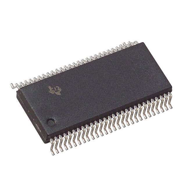
- 型号: SN74ABT16843DLR
- 制造商: Texas Instruments
- 库位|库存: xxxx|xxxx
- 要求:
| 数量阶梯 | 香港交货 | 国内含税 |
| +xxxx | $xxxx | ¥xxxx |
查看当月历史价格
查看今年历史价格
SN74ABT16843DLR产品简介:
ICGOO电子元器件商城为您提供SN74ABT16843DLR由Texas Instruments设计生产,在icgoo商城现货销售,并且可以通过原厂、代理商等渠道进行代购。 SN74ABT16843DLR价格参考。Texas InstrumentsSN74ABT16843DLR封装/规格:逻辑 - 锁销, D-Type Transparent Latch 2 Channel 9:9 IC Tri-State 56-SSOP。您可以下载SN74ABT16843DLR参考资料、Datasheet数据手册功能说明书,资料中有SN74ABT16843DLR 详细功能的应用电路图电压和使用方法及教程。
SN74ABT16843DLR是德州仪器(Texas Instruments)生产的一款16位透明D类锁存器,属于逻辑 - 锁销类产品。该器件广泛应用于需要高速数据锁存与缓冲的数字系统中。

其主要应用场景包括:在高性能计算设备和服务器中,用于地址或数据总线的锁存,以实现时序控制和信号稳定;在通信系统中,作为数据路径管理元件,支持多路信号的同步锁存与传输;在工业自动化控制系统中,用于接口电平转换和数据暂存,提升系统抗干扰能力;此外,还常见于测试测量设备、医疗电子及高可靠性嵌入式系统中,承担关键的数据隔离与驱动功能。

SN74ABT16843DLR采用5.0V工作电压,具备高驱动输出能力和优秀的噪声抑制性能,适合恶劣工业环境。其24位封装(DLR为SSOP形式)节省空间,便于高密度PCB布局。器件支持宽温范围,稳定性强,适用于对可靠性要求较高的场景。

总之,该芯片适用于需高效、稳定进行16位数据锁存与缓冲的各种中高端数字系统,是构建复杂逻辑控制电路的重要组件。
| 参数 | 数值 |
| 产品目录 | 集成电路 (IC) |
| 描述 | IC 18BIT BUS-INT D LATCH 56-SSOP |
| 产品分类 | |
| 品牌 | Texas Instruments |
| 数据手册 | |
| 产品图片 |
|
| 产品型号 | SN74ABT16843DLR |
| rohs | 无铅 / 符合限制有害物质指令(RoHS)规范要求 |
| 产品系列 | 74ABT |
| 供应商器件封装 | 56-SSOP |
| 其它名称 | 296-3932-1 |
| 包装 | 剪切带 (CT) |
| 安装类型 | 表面贴装 |
| 封装/外壳 | 56-BSSOP(0.295",7.50mm 宽) |
| 工作温度 | -40°C ~ 85°C |
| 延迟时间-传播 | 4ns |
| 标准包装 | 1 |
| 独立电路 | 2 |
| 电压-电源 | 4.5 V ~ 5.5 V |
| 电流-输出高,低 | 32mA,64mA |
| 电路 | 9:9 |
| 输出类型 | 三态 |
| 逻辑类型 | D 型透明锁存器 |


- 商务部:美国ITC正式对集成电路等产品启动337调查
- 曝三星4nm工艺存在良率问题 高通将骁龙8 Gen1或转产台积电
- 太阳诱电将投资9.5亿元在常州建新厂生产MLCC 预计2023年完工
- 英特尔发布欧洲新工厂建设计划 深化IDM 2.0 战略
- 台积电先进制程称霸业界 有大客户加持明年业绩稳了
- 达到5530亿美元!SIA预计今年全球半导体销售额将创下新高
- 英特尔拟将自动驾驶子公司Mobileye上市 估值或超500亿美元
- 三星加码芯片和SET,合并消费电子和移动部门,撤换高东真等 CEO
- 三星电子宣布重大人事变动 还合并消费电子和移动部门
- 海关总署:前11个月进口集成电路产品价值2.52万亿元 增长14.8%


PDF Datasheet 数据手册内容提取
SN54ABT16843, SN74ABT16843 18-BIT BUS-INTERFACE D-TYPE LATCHES WITH 3-STATE OUTPUTS SCBS223E – OCTOBER 1992 – REVISED MAY 1997 (cid:1) Members of the Texas Instruments SN54ABT16843...WD PACKAGE Widebus Family SN74ABT16843...DGG OR DL PACKAGE (cid:1) (TOP VIEW) State-of-the-Art EPIC-II B BiCMOS Design Significantly Reduces Power Dissipation 1CLR 1 56 1LE (cid:1) Distributed VCC and GND Pin Configuration 1OE 2 55 1PRE Minimizes High-Speed Switching Noise 1Q1 3 54 1D1 (cid:1) Flow-Through Architecture Optimizes PCB GND 4 53 GND Layout 1Q2 5 52 1D2 (cid:1) High-Impedance State During Power Up 1Q3 6 51 1D3 and Power Down VCC 7 50 VCC (cid:1) 1Q4 8 49 1D4 High-Drive Outputs (–32-mA I , 64-mA I ) OH OL (cid:1) 1Q5 9 48 1D5 Package Options Include Plastic Thin 1Q6 10 47 1D6 Shrink Small-Outline (DGG), 300-mil Shrink GND 11 46 GND Small-Outline (DL) Packages and 380-mil 1Q7 12 45 1D7 Fine-Pitch Ceramic Flat (WD) Package 1Q8 13 44 1D8 Using 25-mil Center-to-Center Spacings 1Q9 14 43 1D9 2Q1 15 42 2D1 description 2Q2 16 41 2D2 The ’ABT16843 18-bit bus-interface D-type 2Q3 17 40 2D3 latches are designed specifically for driving highly GND 18 39 GND capacitive or relatively low-impedance loads. 2Q4 19 38 2D4 They are particularly suitable for implementing 2Q5 20 37 2D5 buffer registers, I/O ports, bidirectional bus 2Q6 21 36 2D6 drivers, and working registers. VCC 22 35 VCC 2Q7 23 34 2D7 The ’ABT16843 can be used as two 9-bit latches 2Q8 24 33 2D8 or one 18-bit latch. The 18 latches are transparent D-type latches. The device provides true data at GND 25 32 GND its outputs. 2Q9 26 31 2D9 2OE 27 30 2PRE A buffered output-enable (OE) input can be used 2CLR 28 29 2LE to place the nine outputs in either a normal logic state (high or low logic levels) or a high-impedance state. The outputs are in the high-impedance state during power up and power down. The outputs remain in the high-impedance state while the device is powered down. In the high-impedance state, the outputs neither load nor drive the bus lines significantly. The high-impedance state and increased drive provide the capability to drive bus lines without need for interface or pullup components. Please be aware that an important notice concerning availability, standard warranty, and use in critical applications of TexasInstruments semiconductor products and disclaimers thereto appears at the end of this data sheet. Widebus and EPIC-II B are trademarks of Texas Instruments Incorporated. UNLESS OTHERWISE NOTED this document contains PRODUCTION Copyright 1997, Texas Instruments Incorporated DATA information current as of publication date. Products conform to specifications per the terms of Texas Instruments standard warranty. Production processing does not necessarily include testing of all parameters. POST OFFICE BOX 655303 • DALLAS, TEXAS 75265 1
SN54ABT16843, SN74ABT16843 18-BIT BUS-INTERFACE D-TYPE LATCHES WITH 3-STATE OUTPUTS SCBS223E – OCTOBER 1992 – REVISED MAY 1997 description (continued) OE does not affect the internal operations of the latch. Previously stored data can be retained or new data can be entered while the outputs are in the high-impedance state. When V is between 0 and 2.1 V, the device is in the high-impedance state during power up or power down. CC However, to ensure the high-impedance state above 2.1 V, OE should be tied to V through a pullup resistor; CC the minimum value of the resistor is determined by the current-sinking capability of the driver. The SN54ABT16843 is characterized for operation over the full military temperature range of –55°C to 125°C. The SN74ABT16843 is characterized for operation from –40°C to 85°C. FUNCTION TABLE (each 9-bit latch) INPUTS OUTPUT PRE CLR OE LE D Q L X L X X H H L L X X L H H L H L L H H L H H H H H L L X Q0 X X H X X Z 2 POST OFFICE BOX 655303 • DALLAS, TEXAS 75265
SN54ABT16843, SN74ABT16843 18-BIT BUS-INTERFACE D-TYPE LATCHES WITH 3-STATE OUTPUTS SCBS223E – OCTOBER 1992 – REVISED MAY 1997 logic diagram (positive logic) 2 1OE 55 1PRE 1 1CLR 56 1LE S2 C1 3 54 1Q1 1D1 1D R To Eight Other Channels 27 2OE 30 2PRE 28 2CLR 29 2LE S2 C1 15 42 2Q1 2D1 1D R To Eight Other Channels POST OFFICE BOX 655303 • DALLAS, TEXAS 75265 3
SN54ABT16843, SN74ABT16843 18-BIT BUS-INTERFACE D-TYPE LATCHES WITH 3-STATE OUTPUTS SCBS223E – OCTOBER 1992 – REVISED MAY 1997 absolute maximum ratings over operating free-air temperature range (unless otherwise noted)† Supply voltage range, V . . . . . . . . . . . . . . . . . . . . . . . . . . . . . . . . . . . . . . . . . . . . . . . . . . . . . . . . . . –0.5 V to 7 V CC Input voltage range, V (see Note 1) . . . . . . . . . . . . . . . . . . . . . . . . . . . . . . . . . . . . . . . . . . . . . . . . . . –0.5 V to 7 V I Voltage range applied to any output in the high or power-off state, V . . . . . . . . . . . . . . . . . . . –0.5 V to 5.5 V O Current into any output in the low state, I : SN54ABT16843 . . . . . . . . . . . . . . . . . . . . . . . . . . . . . . . . . . 96 mA O SN74ABT16843 . . . . . . . . . . . . . . . . . . . . . . . . . . . . . . . . . 128 mA Input clamp current, IIK (VI < 0) . . . . . . . . . . . . . . . . . . . . . . . . . . . . . . . . . . . . . . . . . . . . . . . . . . . . . . . . . . . –18 mA Output clamp current, IOK (VO < 0) . . . . . . . . . . . . . . . . . . . . . . . . . . . . . . . . . . . . . . . . . . . . . . . . . . . . . . . . –50 mA Package thermal impedance, q (see Note 2): DGG package . . . . . . . . . . . . . . . . . . . . . . . . . . . . . . . . 81°C/W JA DL package . . . . . . . . . . . . . . . . . . . . . . . . . . . . . . . . . 74°C/W Storage temperature range, T . . . . . . . . . . . . . . . . . . . . . . . . . . . . . . . . . . . . . . . . . . . . . . . . . . . –65°C to 150°C stg †Stresses beyond those listed under “absolute maximum ratings” may cause permanent damage to the device. These are stress ratings only, and functional operation of the device at these or any other conditions beyond those indicated under “recommended operating conditions” is not implied. Exposure to absolute-maximum-rated conditions for extended periods may affect device reliability. NOTES: 1. The input and output negative-voltage ratings may be exceeded if the input and output clamp-current ratings are observed. 2. The package thermal impedance is calculated in accordance with EIA/JEDEC Std JESD51. recommended operating conditions (see Note 3) SN54ABT16843 SN74ABT16843 UUNNIITT MIN MAX MIN MAX VCC Supply voltage 4.5 5.5 4.5 5.5 V VIH High-level input voltage 2 2 V VIL Low-level input voltage 0.8 0.8 V VI Input voltage 0 VCC 0 VCC V IOH High-level output current –24 –32 mA IOL Low-level output current 48 64 mA D t/D v Input transition rise or fall rate Outputs enabled 10 10 ns/V D t/D VCC Power-up ramp rate 200 200 m s/V TA Operating free-air temperature –55 125 –40 85 °C NOTE 3: Unused inputs must be held high or low to prevent them from floating. PRODUCT PREVIEW information concerns products in the formative or design phase of development. Characteristic data and other specifications are design goals. Texas Instruments reserves the right to change or discontinue these products without notice. 4 POST OFFICE BOX 655303 • DALLAS, TEXAS 75265
SN54ABT16843, SN74ABT16843 18-BIT BUS-INTERFACE D-TYPE LATCHES WITH 3-STATE OUTPUTS SCBS223E – OCTOBER 1992 – REVISED MAY 1997 electrical characteristics over recommended operating free-air temperature range (unless otherwise noted) TA = 25°C SN54ABT16843 SN74ABT16843 PPAARRAAMMEETTEERR TTEESSTT CCOONNDDIITTIIOONNSS UUNNIITT MIN TYP† MAX MIN MAX MIN MAX VIK VCC = 4.5 V, II = –18 mA –1.2 –1.2 –1.2 V VCC = 4.5 V, IOH = –3 mA 2.5 2.5 2.5 VCC = 5 V, IOH = –3 mA 3 3 3 VVOOHH VV IOH = –24 mA 2 2 VVCCCC == 44.55 VV IOH = –32 mA 2* 2 IOL = 48 mA 0.55 0.55 VVOOLL VVCCCC == 44.55 VV VV IOL = 64 mA 0.55* 0.55 Vhys 100 mV II VVCI =C V =C 0C t oo r5 G.5N VD, ±1 ±1 ±1 m A IOZPU‡ VVCOC = =0 .05 tVo 2to.1 2 V.7, V, OE = X ±50 ±50 ±50 m A IOZPD‡ VVCOC = =0 .25. 1V V to t o2 .07, V, OE = X ±50 ±50 ±50 m A IOZH VVCOC = =2 .27. 1V ,V O toE 5≥. 52 VV, 10 10 10 m A IOZL VVCOC = =0 .25. 1V ,V O toE 5≥. 52 VV, –10 –10 –10 m A Ioff VCC = 0, VI or VO ≤ 4.5 V ±100 ±100 m A ICEX Outputs high VCC = 5.5 V, VO = 5.5 V 50 50 50 m A IO§ VCC = 5.5 V, VO = 2.5 V –50 –100 –180 –50 –180 –50 –180 mA Outputs high 0.5 0.5 0.5 ICC Outputs low VVCC = 55.55 VV, IIO = 00, 85 85 85 mA VVII == VVCCCC oorr GGNNDD Outputs disabled 0.5 0.5 0.5 D ICC¶ VOCthCe r= i n5p.5u tVs ,a Ot nVeC iCn pourt GaNt 3D.4 V, 1.5 1.5 1.5 mA Ci VI = 2.5 V or 0.5 V 3.5 pF Co VO = 2.5 V or 0.5 V 8 pF * On products compliant to MIL-PRF-38535, this parameter does not apply. †All typical values are at VCC = 5 V. ‡This parameter is characterized, but not production tested. §Not more than one output should be tested at a time, and the duration of the test should not exceed one second. ¶This is the increase in supply current for each input that is at the specified TTL voltage level rather than VCC or GND. PRODUCT PREVIEW information concerns products in the formative or design phase of development. Characteristic data and other specifications are design goals. Texas Instruments reserves the right to change or discontinue these products without notice. POST OFFICE BOX 655303 • DALLAS, TEXAS 75265 5
SN54ABT16843, SN74ABT16843 18-BIT BUS-INTERFACE D-TYPE LATCHES WITH 3-STATE OUTPUTS SCBS223E – OCTOBER 1992 – REVISED MAY 1997 timing requirements over recommended ranges of supply voltage and operating free-air temperature (unless otherwise noted) (see Figure 1) VCC = 5 V, SN54ABT16843 SN74ABT16843 TA = 25°C UNIT MIN MAX MIN MAX MIN MAX CLR low 3.3 3.3 3.3 tw Pulse duration PRE low 3.3 3.3 3.3 ns LE high 3.3 3.3 3.3 High 0.9 0.9 0.9 ttsu SSeettuupp ttiimmee, ddaattaa bbeeffoorree LLEE↓↓ nnss Low 0.6 0.6 0.6 High 1.7 1.7 1.7 tthh HHoolldd ttiimmee, ddaattaa aafftteerr LLEE↓↓ nnss Low 1.8 1.8 1.8 switching characteristics over recommended ranges of supply voltage and operating free-air temperature, C = 50 pF (unless otherwise noted) (see Figure 1) L VCC = 5 V, PARAMETER FROM TO TA = 25°C SN54ABT16843 SN74ABT16843 UNIT ((IINNPPUUTT)) ((OOUUTTPPUUTT)) MIN TYP MAX MIN MAX MIN MAX tPLH 1.6 3.1 4.2 1.6 5.1 1.6 4.8 DD QQ nnss tPHL 1.6 3.2 4.2 1.6 5 1.6 4.8 tPLH 2.3 4 5 2.3 6.3 2.3 5.9 LLEE QQ nnss tPHL 2.5 3.9 4.8 2.5 5.6 2.5 5.3 tPLH 2.1 4 5.1 2.1 6.3 2.1 6.1 PPRREE QQ nnss tPHL 2.2 3.7 4.6 2.2 5.3 2.2 5 tPLH 1.9 3.7 4.8 1.9 5.7 1.9 5.4 CCLLRR QQ nnss tPHL 2.2 4.2 5.3 2.2 6.1 2.2 6 tPZH 1.6 3.3 4.3 1.6 5.5 1.6 5.4 OOEE QQ nnss tPZL 2 3.2 4.6 2 5.9 2 5.8 tPHZ 1.7 4 5.5 1.7 6.4 1.7 6.3 OOEE QQ nnss tPLZ 1.7 3.7 4.4 1.7 5.3 1.7 5.2 PRODUCT PREVIEW information concerns products in the formative or design phase of development. Characteristic data and other specifications are design goals. Texas Instruments reserves the right to change or discontinue these products without notice. 6 POST OFFICE BOX 655303 • DALLAS, TEXAS 75265
SN54ABT16843, SN74ABT16843 18-BIT BUS-INTERFACE D-TYPE LATCHES WITH 3-STATE OUTPUTS SCBS223E – OCTOBER 1992 – REVISED MAY 1997 PARAMETER MEASUREMENT INFORMATION 7 V 500 W S1 Open From Output TEST S1 Under Test GND tPLH/tPHL Open (sCeeL N= o5t0e pAF) 500 W tPLZ/tPZL 7 V tPHZ/tPZH Open LOAD CIRCUIT 3 V Timing Input 1.5 V 0 V tw tsu th 3 V 3 V Input 1.5 V 1.5 V Data Input 1.5 V 1.5 V 0 V 0 V VOLTAGE WAVEFORMS VOLTAGE WAVEFORMS PULSE DURATION SETUP AND HOLD TIMES 3 V 3 V Output Input 1.5 V 1.5 V 1.5 V 1.5 V Control 0 V 0 V tPZL tPLH tPHL tPLZ Output VOH 3.5 V Waveform 1 Output 1.5 V 1.5 V S1 at 7 V 1.5 V VOL + 0.3 V VOL VOL (see Note B) tPHZ tPHL tPLH tPZH Output VOH VOH Output 1.5 V 1.5 V WSa1v aetf oOrpme n2 1.5 V VOH – 0.3 V VOL (see Note B) ≈ 0 V VOLTAGE WAVEFORMS VOLTAGE WAVEFORMS PROPAGATION DELAY TIMES ENABLE AND DISABLE TIMES INVERTING AND NONINVERTING OUTPUTS LOW- AND HIGH-LEVEL ENABLING NOTES: A. CL includes probe and jig capacitance. B. Waveform 1 is for an output with internal conditions such that the output is low except when disabled by the output control. Waveform2 is for an output with internal conditions such that the output is high except when disabled by the output control. C. All input pulses are supplied by generators having the following characteristics: PRR ≤ 10 MHz, ZO = 50 W , tr ≤ 2.5 ns, tf≤ 2.5 ns. D. The outputs are measured one at a time with one transition per measurement. Figure 1. Load Circuit and Voltage Waveforms POST OFFICE BOX 655303 • DALLAS, TEXAS 75265 7
IMPORTANTNOTICE TexasInstrumentsIncorporated(TI)reservestherighttomakecorrections,enhancements,improvementsandotherchangestoits semiconductorproductsandservicesperJESD46,latestissue,andtodiscontinueanyproductorserviceperJESD48,latestissue.Buyers shouldobtainthelatestrelevantinformationbeforeplacingordersandshouldverifythatsuchinformationiscurrentandcomplete. TI’spublishedtermsofsaleforsemiconductorproducts(http://www.ti.com/sc/docs/stdterms.htm)applytothesaleofpackagedintegrated circuitproductsthatTIhasqualifiedandreleasedtomarket.AdditionaltermsmayapplytotheuseorsaleofothertypesofTIproductsand services. ReproductionofsignificantportionsofTIinformationinTIdatasheetsispermissibleonlyifreproductioniswithoutalterationandis accompaniedbyallassociatedwarranties,conditions,limitations,andnotices.TIisnotresponsibleorliableforsuchreproduced documentation.Informationofthirdpartiesmaybesubjecttoadditionalrestrictions.ResaleofTIproductsorserviceswithstatements differentfromorbeyondtheparametersstatedbyTIforthatproductorservicevoidsallexpressandanyimpliedwarrantiesforthe associatedTIproductorserviceandisanunfairanddeceptivebusinesspractice.TIisnotresponsibleorliableforanysuchstatements. BuyersandotherswhoaredevelopingsystemsthatincorporateTIproducts(collectively,“Designers”)understandandagreethatDesigners remainresponsibleforusingtheirindependentanalysis,evaluationandjudgmentindesigningtheirapplicationsandthatDesignershave fullandexclusiveresponsibilitytoassurethesafetyofDesigners'applicationsandcomplianceoftheirapplications(andofallTIproducts usedinorforDesigners’applications)withallapplicableregulations,lawsandotherapplicablerequirements.Designerrepresentsthat,with respecttotheirapplications,Designerhasallthenecessaryexpertisetocreateandimplementsafeguardsthat(1)anticipatedangerous consequencesoffailures,(2)monitorfailuresandtheirconsequences,and(3)lessenthelikelihoodoffailuresthatmightcauseharmand takeappropriateactions.DesigneragreesthatpriortousingordistributinganyapplicationsthatincludeTIproducts,Designerwill thoroughlytestsuchapplicationsandthefunctionalityofsuchTIproductsasusedinsuchapplications. TI’sprovisionoftechnical,applicationorotherdesignadvice,qualitycharacterization,reliabilitydataorotherservicesorinformation, including,butnotlimitedto,referencedesignsandmaterialsrelatingtoevaluationmodules,(collectively,“TIResources”)areintendedto assistdesignerswhoaredevelopingapplicationsthatincorporateTIproducts;bydownloading,accessingorusingTIResourcesinany way,Designer(individuallyor,ifDesignerisactingonbehalfofacompany,Designer’scompany)agreestouseanyparticularTIResource solelyforthispurposeandsubjecttothetermsofthisNotice. TI’sprovisionofTIResourcesdoesnotexpandorotherwisealterTI’sapplicablepublishedwarrantiesorwarrantydisclaimersforTI products,andnoadditionalobligationsorliabilitiesarisefromTIprovidingsuchTIResources.TIreservestherighttomakecorrections, enhancements,improvementsandotherchangestoitsTIResources.TIhasnotconductedanytestingotherthanthatspecifically describedinthepublisheddocumentationforaparticularTIResource. Designerisauthorizedtouse,copyandmodifyanyindividualTIResourceonlyinconnectionwiththedevelopmentofapplicationsthat includetheTIproduct(s)identifiedinsuchTIResource.NOOTHERLICENSE,EXPRESSORIMPLIED,BYESTOPPELOROTHERWISE TOANYOTHERTIINTELLECTUALPROPERTYRIGHT,ANDNOLICENSETOANYTECHNOLOGYORINTELLECTUALPROPERTY RIGHTOFTIORANYTHIRDPARTYISGRANTEDHEREIN,includingbutnotlimitedtoanypatentright,copyright,maskworkright,or otherintellectualpropertyrightrelatingtoanycombination,machine,orprocessinwhichTIproductsorservicesareused.Information regardingorreferencingthird-partyproductsorservicesdoesnotconstitutealicensetousesuchproductsorservices,orawarrantyor endorsementthereof.UseofTIResourcesmayrequirealicensefromathirdpartyunderthepatentsorotherintellectualpropertyofthe thirdparty,oralicensefromTIunderthepatentsorotherintellectualpropertyofTI. TIRESOURCESAREPROVIDED“ASIS”ANDWITHALLFAULTS.TIDISCLAIMSALLOTHERWARRANTIESOR REPRESENTATIONS,EXPRESSORIMPLIED,REGARDINGRESOURCESORUSETHEREOF,INCLUDINGBUTNOTLIMITEDTO ACCURACYORCOMPLETENESS,TITLE,ANYEPIDEMICFAILUREWARRANTYANDANYIMPLIEDWARRANTIESOF MERCHANTABILITY,FITNESSFORAPARTICULARPURPOSE,ANDNON-INFRINGEMENTOFANYTHIRDPARTYINTELLECTUAL PROPERTYRIGHTS.TISHALLNOTBELIABLEFORANDSHALLNOTDEFENDORINDEMNIFYDESIGNERAGAINSTANYCLAIM, INCLUDINGBUTNOTLIMITEDTOANYINFRINGEMENTCLAIMTHATRELATESTOORISBASEDONANYCOMBINATIONOF PRODUCTSEVENIFDESCRIBEDINTIRESOURCESOROTHERWISE.INNOEVENTSHALLTIBELIABLEFORANYACTUAL, DIRECT,SPECIAL,COLLATERAL,INDIRECT,PUNITIVE,INCIDENTAL,CONSEQUENTIALOREXEMPLARYDAMAGESIN CONNECTIONWITHORARISINGOUTOFTIRESOURCESORUSETHEREOF,ANDREGARDLESSOFWHETHERTIHASBEEN ADVISEDOFTHEPOSSIBILITYOFSUCHDAMAGES. UnlessTIhasexplicitlydesignatedanindividualproductasmeetingtherequirementsofaparticularindustrystandard(e.g.,ISO/TS16949 andISO26262),TIisnotresponsibleforanyfailuretomeetsuchindustrystandardrequirements. WhereTIspecificallypromotesproductsasfacilitatingfunctionalsafetyorascompliantwithindustryfunctionalsafetystandards,such productsareintendedtohelpenablecustomerstodesignandcreatetheirownapplicationsthatmeetapplicablefunctionalsafetystandards andrequirements.Usingproductsinanapplicationdoesnotbyitselfestablishanysafetyfeaturesintheapplication.Designersmust ensurecompliancewithsafety-relatedrequirementsandstandardsapplicabletotheirapplications.DesignermaynotuseanyTIproductsin life-criticalmedicalequipmentunlessauthorizedofficersofthepartieshaveexecutedaspecialcontractspecificallygoverningsuchuse. Life-criticalmedicalequipmentismedicalequipmentwherefailureofsuchequipmentwouldcauseseriousbodilyinjuryordeath(e.g.,life support,pacemakers,defibrillators,heartpumps,neurostimulators,andimplantables).Suchequipmentincludes,withoutlimitation,all medicaldevicesidentifiedbytheU.S.FoodandDrugAdministrationasClassIIIdevicesandequivalentclassificationsoutsidetheU.S. TImayexpresslydesignatecertainproductsascompletingaparticularqualification(e.g.,Q100,MilitaryGrade,orEnhancedProduct). Designersagreethatithasthenecessaryexpertisetoselecttheproductwiththeappropriatequalificationdesignationfortheirapplications andthatproperproductselectionisatDesigners’ownrisk.Designersaresolelyresponsibleforcompliancewithalllegalandregulatory requirementsinconnectionwithsuchselection. DesignerwillfullyindemnifyTIanditsrepresentativesagainstanydamages,costs,losses,and/orliabilitiesarisingoutofDesigner’snon- compliancewiththetermsandprovisionsofthisNotice. MailingAddress:TexasInstruments,PostOfficeBox655303,Dallas,Texas75265 Copyright©2017,TexasInstrumentsIncorporated