ICGOO在线商城 > 集成电路(IC) > 逻辑 - 信号开关,多路复用器,解码器 > SN74F157ADR
 Datasheet下载
- 型号: SN74F157ADR
- 制造商: Texas Instruments
- 库位|库存: xxxx|xxxx
- 要求:
| 数量阶梯 | 香港交货 | 国内含税 |
| +xxxx | $xxxx | ¥xxxx |
查看当月历史价格
查看今年历史价格
SN74F157ADR产品简介:
ICGOO电子元器件商城为您提供SN74F157ADR由Texas Instruments设计生产,在icgoo商城现货销售,并且可以通过原厂、代理商等渠道进行代购。 SN74F157ADR价格参考。Texas InstrumentsSN74F157ADR封装/规格:逻辑 - 信号开关,多路复用器,解码器, Multiplexer 4 x 2:1 16-SOIC。您可以下载SN74F157ADR参考资料、Datasheet数据手册功能说明书,资料中有SN74F157ADR 详细功能的应用电路图电压和使用方法及教程。
SN74F157ADR 是由 Texas Instruments(德州仪器)生产的一款逻辑芯片,属于信号开关和多路复用器系列。该器件主要用作四路 2 输入数据选择器/多路复用器,能够根据输入的控制信号从两组数据中选择一组进行输出。以下是 SN74F157ADR 的一些典型应用场景:

 1. 数据选择与切换
   - 在需要在多个数据源之间进行选择的应用中,SN74F157ADR 可以作为数据选择器使用。例如,在嵌入式系统中,可以通过控制信号选择不同的传感器数据或通信接口信号进行处理。
   - 它可以用于音频、视频或其他信号的切换,确保只有一路信号被传递到后续电路。

 2. 多路复用
   - 在需要将多路输入信号复用到单一路线的应用中,这款芯片非常有用。例如,在微控制器或 FPGA 系统中,可以通过 SN74F157ADR 将多个外围设备的数据复用到一个输入端口。
   - 它还可以用于测试设备中,将多个测试点的信号通过复用器连接到一个测量仪器。

 3. 数字信号处理
   - 在数字信号处理系统中,SN74F157ADR 可以用于选择不同的算法路径或数据流。例如,在数字滤波器或信号处理器中,可以根据需要选择不同的输入数据或参数。

 4. 计算机与外设接口
   - 在早期的计算机系统或工业控制系统中,SN74F157ADR 可用于实现 CPU 和外设之间的数据通道切换。它可以帮助管理多个外设的输入输出信号。
   - 在打印机、扫描仪等外设中,也可以用作数据路径的选择器。

 5. 通信系统
   - 在通信系统中,SN74F157ADR 可用于选择不同的通信信道或协议。例如,在多协议通信模块中,可以选择不同的数据流进行传输或接收。

 6. 教育与实验
   - 由于其功能简单且易于理解,SN74F157ADR 常用于教学和实验环境中,帮助学生学习多路复用器的工作原理以及如何设计基于逻辑门的电路。

 总结
SN74F157ADR 的主要应用场景包括数据选择、信号复用、数字信号处理、计算机接口设计以及通信系统中的信号切换等。它的高速性能(符合 F 系列标准)使其适合需要快速切换的应用场合,同时其简单的逻辑结构也便于集成到复杂的电子系统中。
| 参数 | 数值 |
| 产品目录 | 集成电路 (IC)半导体 |
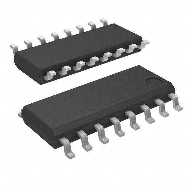
| 描述 | IC QUAD 2-1 DATASELCT/MUX 16SOIC编码器、解码器、复用器和解复用器 Quad 2 to 1 |
| 产品分类 | |
| 品牌 | Texas Instruments |
| 产品手册 | |
| 产品图片 |
|
| rohs | 符合RoHS无铅 / 符合限制有害物质指令(RoHS)规范要求 |
| 产品系列 | 逻辑集成电路,编码器、解码器、复用器和解复用器,Texas Instruments SN74F157ADR74F |
| 数据手册 | |
| 产品型号 | SN74F157ADR |
| 产品 | Selectors / Multiplexers |
| 产品种类 | 编码器、解码器、复用器和解复用器 |
| 传播延迟时间 | 6 ns at 5 V |
| 供应商器件封装 | 16-SOIC N |
| 其它名称 | 296-14808-6 |
| 包装 | Digi-Reel® |
| 单位重量 | 141.700 mg |
| 商标 | Texas Instruments |
| 安装类型 | 表面贴装 |
| 安装风格 | SMD/SMT |
| 封装 | Reel |
| 封装/外壳 | 16-SOIC(0.154",3.90mm 宽) |
| 封装/箱体 | SOIC-16 |
| 工作温度 | 0°C ~ 70°C |
| 工作温度范围 | 0 C to + 70 C |
| 工作电压 | 4.5 V to 5.5 V |
| 工厂包装数量 | 2500 |
| 最大工作温度 | + 70 C |
| 最小工作温度 | 0 C |
| 标准包装 | 1 |
| 独立电路 | 1 |
| 电压-电源 | 4.5 V ~ 5.5 V |
| 电压源 | 单电源 |
| 电流-输出高,低 | 1mA,20mA |
| 电源电压-最大 | 5.5 V |
| 电源电压-最小 | 4.5 V |
| 电路 | 4 x 2:1 |
| 类型 | 多路复用器 |
| 系列 | SN74F157A |
| 输入/输出线数量 | 2 / 1 |
| 输入线路数量 | 2 |
| 输出线路数量 | 1 |
| 逻辑系列 | F |


PDF Datasheet 数据手册内容提取
(cid:1)(cid:2)(cid:3)(cid:4)(cid:5)(cid:6)(cid:3)(cid:7)(cid:8)(cid:9)(cid:10)(cid:1)(cid:2)(cid:7)(cid:4)(cid:5)(cid:6)(cid:3)(cid:7)(cid:8) (cid:11)(cid:12)(cid:8)(cid:13)(cid:14)(cid:12)(cid:15)(cid:16)(cid:17)(cid:10)(cid:18)(cid:19)(cid:16)(cid:20)(cid:2)(cid:17)(cid:10)(cid:21)(cid:22)(cid:10)(cid:6)(cid:19)(cid:16)(cid:20)(cid:2)(cid:17)(cid:10)(cid:13)(cid:8)(cid:21)(cid:8)(cid:10)(cid:1)(cid:17)(cid:16)(cid:17)(cid:23)(cid:21)(cid:22)(cid:14)(cid:1)(cid:24)(cid:25)(cid:12)(cid:16)(cid:21)(cid:20)(cid:15)(cid:16)(cid:17)(cid:26)(cid:17)(cid:14)(cid:1) (cid:27) SDFS053A − MARCH 1987 − REVISED OCTOBER 1993 • Buffered Inputs and Outputs SN54F157A...J PACKAGE • SN74F157A...D OR N PACKAGE Package Options Include Plastic (TOP VIEW) Small-Outline Packages, Ceramic Chip Carriers, and Standard Plastic and Ceramic A/B 1 16 VCC 300-mil DIPs 1A 2 15 G 1B 3 14 4A description 1Y 4 13 4B The ′F157A is a quadruple 2-input data 2A 5 12 4Y selector/multiplexer featuring a common strobe 2B 6 11 3A (G) input. When the strobe is high, all outputs are 2Y 7 10 3B low. When the strobe is low, a 4-bit word is GND 8 9 3Y selected from one of two sources and is routed to the four outputs. The ′F157A provides true data. SN54F157A...FK PACKAGE The SN54F157A is characterized for operation (TOP VIEW) over the full military temperature range of −55°C to 125°C. The SN74F157A is characterized for 1A A/B NCVCCG operation from 0°C to 70°C. 3 2 1 20 19 1B 4 18 4A FUNCTION TABLE 1Y 5 17 4B INPUTS OOUUTTPPUUTT NC 6 16 NC G A/B A B Y 2A 7 15 4Y H X X X L 2B 8 14 3A 9 10 11 12 13 L L L X L L L H X H Y D CY B 2 N N3 3 L H X L L G L H X H H NC − No internal connection (cid:15)(cid:14)(cid:22)(cid:13)(cid:12)(cid:23)(cid:21)(cid:20)(cid:22)(cid:2) (cid:13)(cid:8)(cid:21)(cid:8) (cid:28)(cid:29)(cid:30)(cid:31)!"#$(cid:28)(cid:31)(cid:29) (cid:28)% &’!!((cid:29)$ #% (cid:31)(cid:30) )’*+(cid:28)&#$(cid:28)(cid:31)(cid:29) ,#$(- Copyright 1993, Texas Instruments Incorporated (cid:15)!(cid:31),’&$% &(cid:31)(cid:29)(cid:30)(cid:31)!" $(cid:31) %)(&(cid:28)(cid:30)(cid:28)&#$(cid:28)(cid:31)(cid:29)% )(! $.( $(!"% (cid:31)(cid:30) (cid:21)(/#% (cid:20)(cid:29)%$!’"((cid:29)$% %$#(cid:29),#!, 0#!!#(cid:29)$1- (cid:15)!(cid:31),’&$(cid:28)(cid:31)(cid:29) )!(cid:31)&(%%(cid:28)(cid:29)2 ,(cid:31)(% (cid:29)(cid:31)$ (cid:29)(&(%%#!(cid:28)+1 (cid:28)(cid:29)&+’,( $(%$(cid:28)(cid:29)2 (cid:31)(cid:30) #++ )#!#"($(!%- POST OFFICE BOX 655303 • DALLAS, TEXAS 75265 2−1 • POST OFFICE BOX 1443 HOUSTON, TEXAS 77251−1443
(cid:1)(cid:2)(cid:3)(cid:4)(cid:5)(cid:6)(cid:3)(cid:7)(cid:8)(cid:9)(cid:10)(cid:1)(cid:2)(cid:7)(cid:4)(cid:5)(cid:6)(cid:3)(cid:7)(cid:8) (cid:11)(cid:12)(cid:8)(cid:13)(cid:14)(cid:12)(cid:15)(cid:16)(cid:17)(cid:10)(cid:18)(cid:19)(cid:16)(cid:20)(cid:2)(cid:17)(cid:10)(cid:21)(cid:22)(cid:10)(cid:6)(cid:19)(cid:16)(cid:20)(cid:2)(cid:17)(cid:10)(cid:13)(cid:8)(cid:21)(cid:8)(cid:10)(cid:1)(cid:17)(cid:16)(cid:17)(cid:23)(cid:21)(cid:22)(cid:14)(cid:1)(cid:24)(cid:25)(cid:12)(cid:16)(cid:21)(cid:20)(cid:15)(cid:16)(cid:17)(cid:26)(cid:17)(cid:14)(cid:1) (cid:27) SDFS053A − MARCH 1987 − REVISED OCTOBER 1993 logic symbol† logic diagram (positive logic) 15 2 G EN 1A 1 A/B G1 4 1Y 3 2 1B 1A 1 MUX 4 3 1Y 1B 1 5 5 2A 2A 7 6 2Y 7 2B 6 2Y 11 2B 3A 9 10 3Y 3B 11 14 3A 4A 12 13 4Y 9 4B 10 3Y 3B †This symbol is in accordance with ANSI/IEEE Std 91-1984 and 14 IEC Publication 617-12. 4A Pin numbers shown are for the D, J, and N packages. 12 4Y 13 4B 15 G 1 A/B absolute maximum ratings over operating free-air temperature range (unless otherwise noted)‡ Supply voltage range, V . . . . . . . . . . . . . . . . . . . . . . . . . . . . . . . . . . . . . . . . . . . . . . . . . . . . . . . . . . −0.5 V to 7 V CC Input voltage range (see Note 1) . . . . . . . . . . . . . . . . . . . . . . . . . . . . . . . . . . . . . . . . . . . . . . . . . . . . . −1.2 V to 7 V Input current range . . . . . . . . . . . . . . . . . . . . . . . . . . . . . . . . . . . . . . . . . . . . . . . . . . . . . . . . . . . . . . −30 mA to 5 mA Voltage range applied to any output in the high state . . . . . . . . . . . . . . . . . . . . . . . . . . . . . . . . . . −0.5 V to V CC Current into any output in the low state . . . . . . . . . . . . . . . . . . . . . . . . . . . . . . . . . . . . . . . . . . . . . . . . . . . . . . 40 mA Operating free-air temperature range: SN54F157A . . . . . . . . . . . . . . . . . . . . . . . . . . . . . . . . . . . −55°C to 125°C SN74F157A . . . . . . . . . . . . . . . . . . . . . . . . . . . . . . . . . . . . . . 0°C to 70°C Storage temperature range . . . . . . . . . . . . . . . . . . . . . . . . . . . . . . . . . . . . . . . . . . . . . . . . . . . . . . . . −65°C to 150°C ‡Stresses beyond those listed under “absolute maximum ratings” may cause permanent damage to the device. These are stress ratings only and functional operation of the device at these or any other conditions beyond those indicated under “recommended operating conditions” is not implied. Exposure to absolute-maximum-rated conditions for extended periods may affect device reliability. NOTE 1: The input voltage rating may be exceeded provided that the input current rating is observed. recommended operating conditions SN54F157A SN74F157A UUNNIITT MIN NOM MAX MIN NOM MAX VCC Supply voltage 4.5 5 5.5 4.5 5 5.5 V VIH High-level input voltage 2 2 V VIL Low-level input voltage 0.8 0.8 V IIK Input clamp current −18 −18 mA IOH High-level output current −1 −1 mA IOL Low-level output current 20 20 mA TA Operating free-air temperature −55 125 0 70 °C 2−2 POST OFFICE BOX 65•5303 • DALLAS, TEXAS 75265 POST OFFICE BOX 1443 HOUSTON, TEXAS 77251−1443
(cid:1)(cid:2)(cid:3)(cid:4)(cid:5)(cid:6)(cid:3)(cid:7)(cid:8)(cid:9)(cid:10)(cid:1)(cid:2)(cid:7)(cid:4)(cid:5)(cid:6)(cid:3)(cid:7)(cid:8) (cid:11)(cid:12)(cid:8)(cid:13)(cid:14)(cid:12)(cid:15)(cid:16)(cid:17)(cid:10)(cid:18)(cid:19)(cid:16)(cid:20)(cid:2)(cid:17)(cid:10)(cid:21)(cid:22)(cid:10)(cid:6)(cid:19)(cid:16)(cid:20)(cid:2)(cid:17)(cid:10)(cid:13)(cid:8)(cid:21)(cid:8)(cid:10)(cid:1)(cid:17)(cid:16)(cid:17)(cid:23)(cid:21)(cid:22)(cid:14)(cid:1)(cid:24)(cid:25)(cid:12)(cid:16)(cid:21)(cid:20)(cid:15)(cid:16)(cid:17)(cid:26)(cid:17)(cid:14)(cid:1) (cid:27) SDFS053A − MARCH 1987 − REVISED OCTOBER 1993 electrical characteristics over recommended operating free-air temperature range (unless otherwise noted) SN54F157A SN74F157A PPAARRAAMMEETTEERR TTEESSTT CCOONNDDIITTIIOONNSS UUNNIITT MIN TYP† MAX MIN TYP† MAX VIK VCC = 4.5 V, II = −18 mA −1.2 −1.2 V VCC = 4.5 V, IOH = −1 mA 2.5 3.4 2.5 3.4 VVOOHH VV VCC = 4.75 V, IOH = −1 mA 2.7 VOL VCC = 4.5 V, IOL = 20 mA 0.3 0.5 0.3 0.5 V II VCC = 5.5 V, VI = 7 V 0.1 0.1 mA IIH VCC = 5.5 V, VI = 2.7 V 20 20 µA IIL VCC = 5.5 V, VI = 0.5 V −0.6 −0.6 mA IOS‡ VCC = 5.5 V, VO = 0 −60 −150 −60 −150 mA ICC VCC = 5.5 V, VI = 4.5 V 15 23 15.5 23 mA †All typical values are at VCC = 5 V, TA = 25°C. ‡Not more than one output should be shorted at a time, and the duration of the short circuit should not exceed one second. switching characteristics (see Note 2) VCC = 5 V, VCC = 4.5 V to 5.5 V, CL = 50 pF, CL = 50 pF, FROM TO RL = 500 Ω, RL = 500Ω, PARAMETER ((IINNPPUUTT)) ((OOUUTTPPUUTT)) TA = 25°C TA = MIN to MAX§ UNIT ′F157A SN54F157A SN74F157A MIN TYP MAX MIN MAX MIN MAX tPLH 3.2 6.6 10 3.2 12 3.2 11 AA//BB YY nnss tPHL 2.2 4.6 7 2.2 9 2.2 8 tPLH 4.2 6.6 9.5 4.2 13 4.2 11 GG YY nnss tPHL 1.7 4.1 6.5 1.7 7.5 1.7 7 tPLH 1.7 4.1 6 1.7 7.5 1.7 6.5 AA oorr BB YY nnss tPHL 1.7 3.6 5.5 1 7.5 1.2 7 §For conditions shown as MIN or MAX, use the appropriate value specified under recommended operating conditions. NOTE 2: Load circuits and voltage waveforms are shown in Section 1. POST OFFICE BOX 65•5303 • DALLAS, TEXAS 75265 2−3 POST OFFICE BOX 1443 HOUSTON, TEXAS 77251−1443
(cid:1)(cid:2)(cid:3)(cid:4)(cid:5)(cid:6)(cid:3)(cid:7)(cid:8)(cid:9)(cid:10)(cid:1)(cid:2)(cid:7)(cid:4)(cid:5)(cid:6)(cid:3)(cid:7)(cid:8) (cid:11)(cid:12)(cid:8)(cid:13)(cid:14)(cid:12)(cid:15)(cid:16)(cid:17)(cid:10)(cid:18)(cid:19)(cid:16)(cid:20)(cid:2)(cid:17)(cid:10)(cid:21)(cid:22)(cid:10)(cid:6)(cid:19)(cid:16)(cid:20)(cid:2)(cid:17)(cid:10)(cid:13)(cid:8)(cid:21)(cid:8)(cid:10)(cid:1)(cid:17)(cid:16)(cid:17)(cid:23)(cid:21)(cid:22)(cid:14)(cid:1)(cid:24)(cid:25)(cid:12)(cid:16)(cid:21)(cid:20)(cid:15)(cid:16)(cid:17)(cid:26)(cid:17)(cid:14)(cid:1) (cid:27) SDFS053A − MARCH 1987 − REVISED OCTOBER 1993 2−4 POST OFFICE BOX 65•5303 • DALLAS, TEXAS 75265 POST OFFICE BOX 1443 HOUSTON, TEXAS 77251−1443
IMPORTANTNOTICE TexasInstrumentsIncorporatedanditssubsidiaries(TI)reservetherighttomakecorrections,modifications,enhancements,improvements, andotherchangestoitsproductsandservicesatanytimeandtodiscontinueanyproductorservicewithoutnotice.Customersshould obtainthelatestrelevantinformationbeforeplacingordersandshouldverifythatsuchinformationiscurrentandcomplete.Allproductsare soldsubjecttoTI’stermsandconditionsofsalesuppliedatthetimeoforderacknowledgment. TIwarrantsperformanceofitshardwareproductstothespecificationsapplicableatthetimeofsaleinaccordancewithTI’sstandard warranty.TestingandotherqualitycontroltechniquesareusedtotheextentTIdeemsnecessarytosupportthiswarranty.Exceptwhere mandatedbygovernmentrequirements,testingofallparametersofeachproductisnotnecessarilyperformed. TIassumesnoliabilityforapplicationsassistanceorcustomerproductdesign.Customersareresponsiblefortheirproductsand applicationsusingTIcomponents.Tominimizetherisksassociatedwithcustomerproductsandapplications,customersshouldprovide adequatedesignandoperatingsafeguards. TIdoesnotwarrantorrepresentthatanylicense,eitherexpressorimplied,isgrantedunderanyTIpatentright,copyright,maskworkright, orotherTIintellectualpropertyrightrelatingtoanycombination,machine,orprocessinwhichTIproductsorservicesareused.Information publishedbyTIregardingthird-partyproductsorservicesdoesnotconstitutealicensefromTItousesuchproductsorservicesora warrantyorendorsementthereof.Useofsuchinformationmayrequirealicensefromathirdpartyunderthepatentsorotherintellectual propertyofthethirdparty,oralicensefromTIunderthepatentsorotherintellectualpropertyofTI. ReproductionofTIinformationinTIdatabooksordatasheetsispermissibleonlyifreproductioniswithoutalterationandisaccompanied byallassociatedwarranties,conditions,limitations,andnotices.Reproductionofthisinformationwithalterationisanunfairanddeceptive businesspractice.TIisnotresponsibleorliableforsuchaltereddocumentation.Informationofthirdpartiesmaybesubjecttoadditional restrictions. ResaleofTIproductsorserviceswithstatementsdifferentfromorbeyondtheparametersstatedbyTIforthatproductorservicevoidsall expressandanyimpliedwarrantiesfortheassociatedTIproductorserviceandisanunfairanddeceptivebusinesspractice.TIisnot responsibleorliableforanysuchstatements. TIproductsarenotauthorizedforuseinsafety-criticalapplications(suchaslifesupport)whereafailureoftheTIproductwouldreasonably beexpectedtocauseseverepersonalinjuryordeath,unlessofficersofthepartieshaveexecutedanagreementspecificallygoverning suchuse.Buyersrepresentthattheyhaveallnecessaryexpertiseinthesafetyandregulatoryramificationsoftheirapplications,and acknowledgeandagreethattheyaresolelyresponsibleforalllegal,regulatoryandsafety-relatedrequirementsconcerningtheirproducts andanyuseofTIproductsinsuchsafety-criticalapplications,notwithstandinganyapplications-relatedinformationorsupportthatmaybe providedbyTI.Further,BuyersmustfullyindemnifyTIanditsrepresentativesagainstanydamagesarisingoutoftheuseofTIproductsin suchsafety-criticalapplications. TIproductsareneitherdesignednorintendedforuseinmilitary/aerospaceapplicationsorenvironmentsunlesstheTIproductsare specificallydesignatedbyTIasmilitary-gradeor"enhancedplastic."OnlyproductsdesignatedbyTIasmilitary-grademeetmilitary specifications.BuyersacknowledgeandagreethatanysuchuseofTIproductswhichTIhasnotdesignatedasmilitary-gradeissolelyat theBuyer'srisk,andthattheyaresolelyresponsibleforcompliancewithalllegalandregulatoryrequirementsinconnectionwithsuchuse. TIproductsareneitherdesignednorintendedforuseinautomotiveapplicationsorenvironmentsunlessthespecificTIproductsare designatedbyTIascompliantwithISO/TS16949requirements.Buyersacknowledgeandagreethat,iftheyuseanynon-designated productsinautomotiveapplications,TIwillnotberesponsibleforanyfailuretomeetsuchrequirements. FollowingareURLswhereyoucanobtaininformationonotherTexasInstrumentsproductsandapplicationsolutions: Products Applications Amplifiers amplifier.ti.com Audio www.ti.com/audio DataConverters dataconverter.ti.com Automotive www.ti.com/automotive DSP dsp.ti.com Broadband www.ti.com/broadband ClocksandTimers www.ti.com/clocks DigitalControl www.ti.com/digitalcontrol Interface interface.ti.com Medical www.ti.com/medical Logic logic.ti.com Military www.ti.com/military PowerMgmt power.ti.com OpticalNetworking www.ti.com/opticalnetwork Microcontrollers microcontroller.ti.com Security www.ti.com/security RFID www.ti-rfid.com Telephony www.ti.com/telephony RF/IFandZigBee®Solutions www.ti.com/lprf Video&Imaging www.ti.com/video Wireless www.ti.com/wireless MailingAddress:TexasInstruments,PostOfficeBox655303,Dallas,Texas75265 Copyright©2008,TexasInstrumentsIncorporated