ICGOO在线商城 > 集成电路(IC) > 逻辑 - 信号开关,多路复用器,解码器 > SN74LVC138AD
 Datasheet下载
- 型号: SN74LVC138AD
- 制造商: Texas Instruments
- 库位|库存: xxxx|xxxx
- 要求:
| 数量阶梯 | 香港交货 | 国内含税 |
| +xxxx | $xxxx | ¥xxxx |
查看当月历史价格
查看今年历史价格
SN74LVC138AD产品简介:
ICGOO电子元器件商城为您提供SN74LVC138AD由Texas Instruments设计生产,在icgoo商城现货销售,并且可以通过原厂、代理商等渠道进行代购。 SN74LVC138AD价格参考。Texas InstrumentsSN74LVC138AD封装/规格:逻辑 - 信号开关,多路复用器,解码器, Decoder/Demultiplexer 1 x 3:8 16-SOIC。您可以下载SN74LVC138AD参考资料、Datasheet数据手册功能说明书,资料中有SN74LVC138AD 详细功能的应用电路图电压和使用方法及教程。
SN74LVC138AD是Texas Instruments(德州仪器)生产的一款3线-8线解码器/译码器,属于逻辑信号开关和多路复用器系列。它在数字电路设计中广泛应用,尤其适用于需要将少量输入信号转换为多个输出信号的场景。以下是该型号的主要应用场景:

 1. 地址解码
   SN74LVC138AD常用于微处理器或微控制器系统中的地址解码。通过将3位地址线(A0、A1、A2)转换为8个独立的输出信号,它可以有效地选择8个不同的存储器或外围设备地址。这种应用常见于嵌入式系统、单片机扩展、以及多芯片系统的地址管理。

 2. 多路选择与控制
   在多路复用器和多路选择器的应用中,SN74LVC138AD可以用于从多个输入源中选择一个特定的输出通道。例如,在音频或视频切换系统中,它可以用于选择不同的输入信号源,并将其路由到指定的输出端口。

 3. I/O扩展
   该器件还可以用于扩展微控制器的I/O引脚。当微控制器的I/O资源有限时,可以通过SN74LVC138AD将3个控制引脚扩展为8个独立的输出引脚,从而实现更多的外设控制功能。

 4. LED显示驱动
   在LED显示器或多段LED驱动中,SN74LVC138AD可以用于控制多个LED灯或数码管的点亮。通过解码输入信号,它可以依次选择不同的LED段或位,实现动态显示效果。

 5. 传感器数据采集
   在多传感器数据采集系统中,SN74LVC138AD可以用于选择不同的传感器通道,将来自多个传感器的数据依次传输到微控制器进行处理。这在工业自动化、环境监测等领域非常有用。

 6. 电源管理
   在一些电源管理系统中,SN74LVC138AD可以用于控制多个电源模块的开启或关闭。通过解码输入信号,它可以精确地控制不同电源路径的通断,优化系统的功耗管理。

总之,SN74LVC138AD凭借其高效、可靠的解码功能,广泛应用于各种数字电路和控制系统中,尤其是在需要对多路信号进行选择和控制的场合。
| 参数 | 数值 |
| 产品目录 | 集成电路 (IC)半导体 |
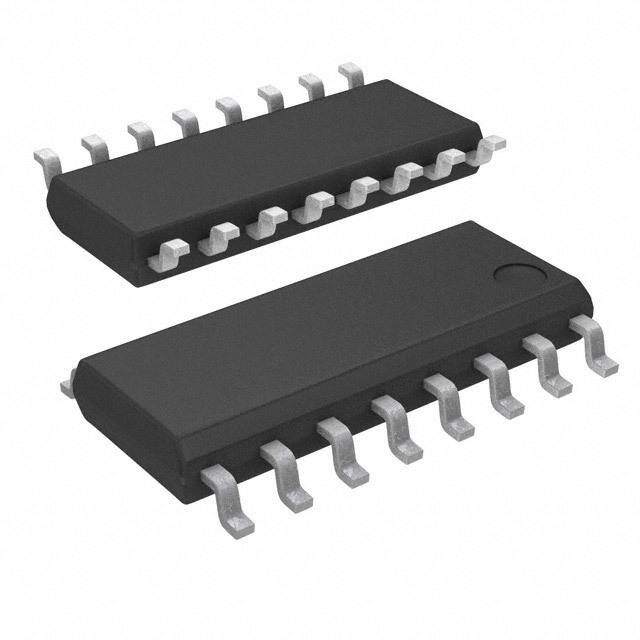
| 描述 | IC 3-TO-8 DECOD/DEMUX 16-SOIC编码器、解码器、复用器和解复用器 Line Decoder |
| 产品分类 | |
| 品牌 | Texas Instruments |
| 产品手册 | http://www.ti.com/lit/gpn/sn74lvc138a |
| 产品图片 |
|
| rohs | 符合RoHS无铅 / 符合限制有害物质指令(RoHS)规范要求 |
| 产品系列 | 逻辑集成电路,编码器、解码器、复用器和解复用器,Texas Instruments SN74LVC138AD74LVC |
| 数据手册 | |
| 产品型号 | SN74LVC138AD |
| 产品 | Decoders / Demultiplexers |
| 产品目录页面 | |
| 产品种类 | 编码器、解码器、复用器和解复用器 |
| 传播延迟时间 | 5.8 ns |
| 供应商器件封装 | 16-SOIC N |
| 其它名称 | 296-8459-5 |
| 功率耗散 | 200 mW |
| 包装 | 管件 |
| 单位重量 | 141.700 mg |
| 商标 | Texas Instruments |
| 安装类型 | 表面贴装 |
| 安装风格 | SMD/SMT |
| 封装 | Tube |
| 封装/外壳 | 16-SOIC(0.154",3.90mm 宽) |
| 封装/箱体 | SOIC-16 |
| 工作温度 | -40°C ~ 85°C |
| 工作温度范围 | - 40 C to + 85 C |
| 工作电压 | 2 V to 3.6 V |
| 工厂包装数量 | 40 |
| 最大工作温度 | + 85 C |
| 最小工作温度 | - 40 C |
| 标准包装 | 40 |
| 独立电路 | 1 |
| 电压-电源 | 1.65 V ~ 3.6 V |
| 电压源 | 单电源 |
| 电流-输出高,低 | 24mA,24mA |
| 电源电压-最大 | 3.6 V |
| 电源电压-最小 | 2 V |
| 电路 | 1 x 3:8 |
| 类型 | 解码器/多路分解器 |
| 系列 | SN74LVC138A |
| 输入/输出线数量 | 3 / 8 |
| 输入线路数量 | 3 |
| 输出线路数量 | 8 |
| 逻辑系列 | LVC |


- 商务部:美国ITC正式对集成电路等产品启动337调查
- 曝三星4nm工艺存在良率问题 高通将骁龙8 Gen1或转产台积电
- 太阳诱电将投资9.5亿元在常州建新厂生产MLCC 预计2023年完工
- 英特尔发布欧洲新工厂建设计划 深化IDM 2.0 战略
- 台积电先进制程称霸业界 有大客户加持明年业绩稳了
- 达到5530亿美元!SIA预计今年全球半导体销售额将创下新高
- 英特尔拟将自动驾驶子公司Mobileye上市 估值或超500亿美元
- 三星加码芯片和SET,合并消费电子和移动部门,撤换高东真等 CEO
- 三星电子宣布重大人事变动 还合并消费电子和移动部门
- 海关总署:前11个月进口集成电路产品价值2.52万亿元 增长14.8%


PDF Datasheet 数据手册内容提取
Product Sample & Technical Tools & Support & Folder Buy Documents Software Community SN54LVC138A,SN74LVC138A SCAS291W–MARCH1993–REVISEDOCTOBER2016 SN74LVC138A 3-Line to 8-Line Decoders Demultiplexers 1 Features 3 Description • OperateFrom1.65Vto3.6V The SN74LVC138A devices are designed for high- 1 performance memory-decoding or data-routing • InputsAcceptVoltagesto5.5V applications requiring very short propagation delay • Maxtpdof5.8nsat3.3V times. In high-performance memory systems, these • TypicalV (OutputGroundBounce) decoders minimize the effects of system decoding. OLP <0.8VatV =3.3V,T =25°C When employed with high-speed memories using a CC A fast enable circuit, delay times of these decoders and • TypicalV (OutputV Undershoot) OHV OH the enable time of the memory usually are less than >2VatV =3.3V,T =25°C CC A the typical access time of the memory. This means • Latch-UpPerformanceExceeds250mAPer that the effective system delay introduced by the JESD17 decodersisnegligible. 2 Applications DeviceInformation(1) PARTNUMBER PACKAGE BODYSIZE(NOM) • LEDDisplays LCCC(20) 8.89mm×8.89mm • Servers CDIP(16) 19.56mm×6.92mm • WhiteGoods CFP(16) 10.30mm×6.73mm • PowerInfrastructure SOIC(16) 9.90mm×3.91mm • BuildingAutomation SSOP(16) 6.20mm×5.30mm SNx4LVC138A • FactoryAutomation TVSOP(16) 3.60mm×4.40mm BGAMICROSTAR 4.00mm×3.00mm JUNIOR(20) TSSOP(16) 5.00mm×4.40mm UQFN(16) 2.60mm×1.80mm (1) For all available packages, see the orderable addendum at theendofthedatasheet. LogicDiagram(PositiveLogic) 15 Y0 1 A 14 Y1 Select 2 Inputs B 13 Y2 3 12 C Y3 Data Outputs 11 Y4 10 Y5 6 G1 9 Y6 EInnpaubtlse G2A 4 7 Y7 5 G2B Pin numbers shown are for the D, DB, DGV, J, NS, PW, RGY, and W packages. Copyright©2016,TexasInstrumentsIncorporated 1 An IMPORTANT NOTICE at the end of this data sheet addresses availability, warranty, changes, use in safety-critical applications, intellectualpropertymattersandotherimportantdisclaimers.PRODUCTIONDATA.
SN54LVC138A,SN74LVC138A SCAS291W–MARCH1993–REVISEDOCTOBER2016 www.ti.com Table of Contents 1 Features.................................................................. 1 8.2 FunctionalBlockDiagram.......................................10 2 Applications........................................................... 1 8.3 FeatureDescription.................................................10 3 Description............................................................. 1 8.4 DeviceFunctionalModes........................................11 4 RevisionHistory..................................................... 2 9 ApplicationandImplementation........................ 12 9.1 ApplicationInformation............................................12 5 PinConfigurationandFunctions......................... 3 9.2 TypicalApplication..................................................12 6 Specifications......................................................... 5 10 PowerSupplyRecommendations..................... 13 6.1 AbsoluteMaximumRatings......................................5 11 Layout................................................................... 13 6.2 ESDRatings..............................................................5 6.3 RecommendedOperatingConditions.......................6 11.1 LayoutGuidelines.................................................13 6.4 ThermalInformation..................................................6 11.2 LayoutExample....................................................13 6.5 ElectricalCharacteristics...........................................7 12 DeviceandDocumentationSupport................. 14 6.6 SwitchingCharacteristics—SN54LVC138A..............7 12.1 RelatedLinks........................................................14 6.7 SwitchingCharacteristics—SN74LVC138A..............7 12.2 ReceivingNotificationofDocumentationUpdates14 6.8 OperatingCharacteristics..........................................8 12.3 CommunityResources..........................................14 6.9 TypicalCharacteristics..............................................8 12.4 Trademarks...........................................................14 7 ParameterMeasurementInformation..................9 12.5 ElectrostaticDischargeCaution............................14 12.6 Glossary................................................................14 8 DetailedDescription............................................ 10 13 Mechanical,Packaging,andOrderable 8.1 Overview.................................................................10 Information........................................................... 14 4 Revision History NOTE:Pagenumbersforpreviousrevisionsmaydifferfrompagenumbersinthecurrentversion. ChangesfromRevisionV(November2013)toRevisionW Page • AddedESDRatingstable,FeatureDescriptionsection,DeviceFunctionalModes,ApplicationandImplementation section,PowerSupplyRecommendationssection,Layoutsection,DeviceandDocumentationSupportsection,and Mechanical,Packaging,andOrderableInformationsection ................................................................................................. 1 • DeletedOrderingInformationtable;seePackagingOrderingAddendumattheendofthedatasheet................................ 1 • ChangedR valuesfrom:73to86.8(D),82to100.1(DB),120to122.1(DGV),78to84(ZQN),108to108.9 θJA (PW)....................................................................................................................................................................................... 6 • DeletedR valuesforNSandRGYpackages..................................................................................................................... 6 θJA ChangesfromRevisionU(OCTOBER2012)toRevisionV Page • UpdateddocumenttonewTIdatasheetformat-nospecificationchanges......................................................................... 1 • RemovedOrderingInformationtable..................................................................................................................................... 1 • AddedESDwarning............................................................................................................................................................... 1 2 SubmitDocumentationFeedback Copyright©1993–2016,TexasInstrumentsIncorporated ProductFolderLinks:SN54LVC138A SN74LVC138A
SN54LVC138A,SN74LVC138A www.ti.com SCAS291W–MARCH1993–REVISEDOCTOBER2016 5 Pin Configuration and Functions SN54LVC138A...J OR W PACKAGE SN74LVC138A...D, DB, DGV, NS, SN54LVC138A...FK PACKAGE OR PW PACKAGE (TOPVIEW) (TOPVIEW) C C C0 BAN V Y A 1 16 VCC 3 2 1 20 19 B 2 15 Y0 C 4 18 Y1 C 3 14 Y1 G2A 5 17 Y2 G2A 4 13 Y2 NC 6 16 NC G2B 5 12 Y3 G2B 7 15 Y3 G1 6 11 Y4 G1 8 14 Y4 Y7 7 10 Y5 9 10 11 12 13 GND 8 9 Y6 7D C 6 5 YN N Y Y G NC - No internal connection SN74LVC138A...RGY PACKAGE (TOPVIEW) C SN54LVC138A...RSVPACKAGE A VC (TOPVIEW) 1 16 3 4 5 6 Y Y Y Y B 2 15 Y0 12 11 10 9 C 3 14 Y1 Y2 13 8 GND G2A 4 13 Y2 Y1 14 7 Y7 G2B 5 12 Y3 Y0 15 6 G1 G1 6 11 Y4 Y7 7 10 Y5 VCC 16 5 G2B 1 2 3 4 8 9 A B C A ND Y6 2G G GQNORZQNPACKAGE (TOPVIEW) 1 2 3 4 A B C D E Table1.PinAssignmentsforZQN(BGA) 1 2 3 4 A B A V Y0 CC B C NC(1) NC(1) Y1 C G2B G2A Y3 Y2 D G1 NC(1) NC(1) Y4 E GND Y7 Y6 Y5 (1) NC-Nointernalconnection Copyright©1993–2016,TexasInstrumentsIncorporated SubmitDocumentationFeedback 3 ProductFolderLinks:SN54LVC138A SN74LVC138A
SN54LVC138A,SN74LVC138A SCAS291W–MARCH1993–REVISEDOCTOBER2016 www.ti.com PinFunctions PIN SOIC,SSOP, TVSOP,SO, BGA DESCRIPTION NAME LCCC MICROSTAR I/O TSSOP, JUNIOR VQFN,UQFN A 1 2 A2 I SelectinputA(leastsignificantbit) B 2 3 A1 I SelectinputB C 3 4 B1 I SelectinputC(mostsignificantbit) G2A 4 5 C2 I ActivelowenableA G2B 5 7 C1 I ActivelowenableB G1 6 8 D1 I Activehighenable GND 8 10 E1 — Ground NC — 1,11,16 B2,B3,D2,D3 — Nointernalconnection V 16 20 A3 — Supplyvoltage CC Y0 15 19 A4 O Output0(leastsignificantbit) Y1 14 18 B4 O Output1 Y2 13 17 C4 O Output2 Y3 12 15 C3 O Output3 Y4 11 14 D4 O Output4 Y5 10 13 E4 O Output5 Y6 9 12 E3 O Output6 Y7 7 9 E2 O Output7(mostsignificantbit) 4 SubmitDocumentationFeedback Copyright©1993–2016,TexasInstrumentsIncorporated ProductFolderLinks:SN54LVC138A SN74LVC138A
SN54LVC138A,SN74LVC138A www.ti.com SCAS291W–MARCH1993–REVISEDOCTOBER2016 6 Specifications 6.1 Absolute Maximum Ratings overoperatingfree-airtemperaturerange(unlessotherwisenoted)(1) MIN MAX UNIT V Supplyvoltage –0.5 6.5 V CC V Inputvoltage(2) –0.5 6.5 V I V Outputvoltage(2)(3) –0.5 V +0.5 V O CC I Inputclampcurrent V <0 –50 mA IK I I Outputclampcurrent V <0 –50 mA OK O I Continuousoutputcurrent ±50 mA O ContinuouscurrentthroughV orGND ±100 mA CC T Storagetemperature –65 150 °C stg T Junctiontemperature 150 °C J (1) StressesbeyondthoselistedunderAbsoluteMaximumRatingsmaycausepermanentdamagetothedevice.Thesearestressratings only,whichdonotimplyfunctionaloperationofthedeviceattheseoranyotherconditionsbeyondthoseindicatedunderRecommended OperatingConditions.Exposuretoabsolute-maximum-ratedconditionsforextendedperiodsmayaffectdevicereliability. (2) Theinputandoutputnegative-voltageratingsmaybeexceedediftheinputandoutputcurrentratingsareobserved. (3) ThevalueofV isprovidedintherecommendedoperatingconditionstable. CC 6.2 ESD Ratings VALUE UNIT Human-bodymodel(HBM),perANSI/ESDA/JEDECJS-001(1) 2000 Charged-devicemodel(CDM),perJEDECspecificationJESD22- V(ESD) Electrostaticdischarge C101(2) 1000 V Machinemodel(MM) 200 (1) JEDECdocumentJEP155statesthat500-VHBMallowssafemanufacturingwithastandardESDcontrolprocess. (2) JEDECdocumentJEP157statesthat250-VCDMallowssafemanufacturingwithastandardESDcontrolprocess. Copyright©1993–2016,TexasInstrumentsIncorporated SubmitDocumentationFeedback 5 ProductFolderLinks:SN54LVC138A SN74LVC138A
SN54LVC138A,SN74LVC138A SCAS291W–MARCH1993–REVISEDOCTOBER2016 www.ti.com 6.3 Recommended Operating Conditions MIN MAX UNIT SN54LVC138A(1) 2 3.6 Operating V Supplyvoltage SN74LVC138A(1) 1.65 3.6 V CC Dataretentiononly 1.5 V =1.65Vto1.95V SN74LVC138A(1) 0.65× CC V CC VIH High-levelinputvoltage V =2.3Vto2.7V SN74LVC138A(1) 1.7 V CC V =2.7Vto3.6V 2 CC V =1.65Vto1.95V SN74LVC138A(1) 0.35× CC V CC VIL Low-levelinputvoltage V =2.3Vto2.7V SN74LVC138A(1) 0.7 V CC V =2.7Vto3.6V 0.8 CC V Inputvoltage 0 5.5 V I V Outputvoltage 0 V V O CC V =1.65V SN74LVC138A(1) –4 CC V =2.3V SN74LVC138A(1) –8 CC I High-leveloutputcurrent mA OH V =2.7V –12 CC V =3V –24 CC V =1.65V SN74LVC138A(1) 4 CC V =2.3V SN74LVC138A(1) 8 CC I Low-leveloutputcurrent mA OL V =2.7V 12 CC V =3V 24 CC Δt/Δv Inputtransitionriseorfallrate 10 ns/V Operatingfree-air SN54LVC138A(1) –55 125 T °C A temperature SN74LVC138A(1) –40 85 (1) AllunusedinputsofthedevicemustbeheldatV orGNDtoensureproperdeviceoperation.SeetheTIapplicationreport, CC ImplicationsofSloworFloatingCMOSInputs. 6.4 Thermal Information SNx4LVC138A ZQN FK J W D DB DGV (BGA PW RSV THERMALMETRIC(1) (LCCC) (CDIP) (CFP) (SOIC) (SSOP) (TVSOP) MICROSTAR (TSSOP) (UQFN) UNIT JUNIOR) 20 16 16 16 16 16 20 16 16 PINS PINS PINS PINS PINS PINS PINS PINS PINS Junction-to-ambientthermal RθJA resistance 79.2 85.8 138.0 86.8 100.1 122.1 84 108.9 168.9 °C/W Junction-to-case(top)thermal RθJC(top) resistance 56.5 49.3 74.6 47.9 50.6 47.4 56.9 42.5 78.2 °C/W Junction-to-boardthermal RθJB resistance 55.2 64.9 127.7 43.8 50.7 53.8 46.1 54.5 96.4 °C/W Junction-to-topcharacterization ψJT parameter 49.8 37.4 50 15.7 14.3 4.6 3 4.4 4.2 °C/W Junction-to-board ψJB characterizationparameter 55.0 69.5 115.7 43.5 50.1 53.2 48.9 53.8 96.5 °C/W (1) Formoreinformationabouttraditionalandnewthermalmetrics,seetheSemiconductorandICPackageThermalMetricsapplication report. 6 SubmitDocumentationFeedback Copyright©1993–2016,TexasInstrumentsIncorporated ProductFolderLinks:SN54LVC138A SN74LVC138A
SN54LVC138A,SN74LVC138A www.ti.com SCAS291W–MARCH1993–REVISEDOCTOBER2016 6.5 Electrical Characteristics overrecommendedoperatingfree-airtemperaturerange(unlessotherwisenoted) PARAMETER TESTCONDITIONS VCC MIN TYP(1) MAX UNIT SN74LVC138A 1.65Vto3.6V VCC–0.2 IOH=–100µA SN54LVC138A 2.7Vto3.6V VCC–0.2 IOH=–4mA SN74LVC138A 1.65V 1.2 VOH High-leveloutputvoltage IOH=–8mA SN74LVC138A 2.3V 1.7 V 2.7V 2.2 IOH=–12mA 3V 2.4 IOH=–24mA 3V 2.2 SN74LVC138A 1.65Vto3.6V 0.2 IOL=100µA SN54LVC138A 2.7Vto3.6V 0.2 IOL=4mA SN74LVC138A 1.65V 0.45 VOL Low-leveloutputvoltage V IOL=8mA SN74LVC138A 2.3V 0.7 IOL=12mA 2.7V 0.4 IOL=24mA 3V 0.55 II Inputcurrent VI=5.5VorGND 3.6V ±5 µA ICC Supplycurrent VI=VCCorGND,IO=0 3.6V 10 µA ΔICC Changeinsupplycurrent OOntheerinipnuptuatstaVtCVCC–C0o.r6GVN,D 2.7Vto3.6V 500 µA Ci Inputcapacitance VI=VCCorGND 3.3V 5 pF (1) AlltypicalvaluesareatV =3.3V,T =25°C. CC A 6.6 Switching Characteristics—SN54LVC138A overrecommendedoperatingfree-airtemperaturerange(unlessotherwisenoted)(seeFigure2) FROM TO PARAMETER TESTCONDITIONS MIN MAX UNIT (INPUT) (OUTPUT) VCC=2.7V 7.9 AorBorC VCC=3.3V±0.3V 1 6.7 VCC=2.7V 7.4 tpd Propagation(delay)time G2AorG2B Y ns VCC=3.3V±0.3V 1 6.5 VCC=2.7V 6.4 G1 VCC=3.3V±0.3V 1 5.8 6.7 Switching Characteristics—SN74LVC138A overrecommendedoperatingfree-airtemperaturerange(unlessotherwisenoted)(seeFigure2) FROM TO PARAMETER TESTCONDITIONS MIN MAX UNIT (INPUT) (OUTPUT) VCC=1.8V±0.15V 1 22 VCC=2.5V±0.2V 1 9.9 AorBorC VCC=2.7V 1 7.9 VCC=3.3V±0.3V 1 6.7 VCC=1.8V±0.15V 1 21 VCC=2.5V±0.2V 1 9.4 tpd Propagation(delay)time G2AorG2B Y ns VCC=2.7V 1 7.4 VCC=3.3V±0.3V 1 6.5 VCC=1.8V±0.15V 1 20.3 VCC=2.5V±0.2V 1 8.4 G1 VCC=2.7V 1 6.4 VCC=3.3V±0.3V 1 5.8 tsk(o) Skew(time),output — — VCC=3.3V±0.3V 1 ns Copyright©1993–2016,TexasInstrumentsIncorporated SubmitDocumentationFeedback 7 ProductFolderLinks:SN54LVC138A SN74LVC138A
SN54LVC138A,SN74LVC138A SCAS291W–MARCH1993–REVISEDOCTOBER2016 www.ti.com 6.8 Operating Characteristics T =25°C A PARAMETER TESTCONDITIONS TYP UNIT V =1.8V 25 CC C Powerdissipationcapacitance f=10MHz V =2.5V 26 pF pd CC V =3.3V 27 CC 6.9 Typical Characteristics 24 s) Y (n 22 o 20 A t y - 18 a el 16 D on 14 ati g 12 a p Pro 10 m u 8 m xi 6 a M 4 1.8 2 2.2 2.4 2.6 2.8 3 3.2 3.4 Supply Voltage VCC (V) D002 Figure1.MaximumPropagationDelayvsSupplyVoltage 8 SubmitDocumentationFeedback Copyright©1993–2016,TexasInstrumentsIncorporated ProductFolderLinks:SN54LVC138A SN74LVC138A
SN54LVC138A,SN74LVC138A www.ti.com SCAS291W–MARCH1993–REVISEDOCTOBER2016 7 Parameter Measurement Information VLOAD From Output RL S1 Open TEST S1 Under Test GND tPLH/tPHL Open (see NoteCAL) RL tPLZ/tPZL VLOAD tPHZ/tPZH GND LOAD CIRCUIT INPUTS VCC VI tr/tf VM VLOAD CL RL VD 1.8 V±0.15 V VCC ≤2 ns VCC/2 2×VCC 30 pF 1 kW 0.15 V 2.5 V±0.2 V VCC ≤2 ns VCC/2 2×VCC 30 pF 500W 0.15 V 2.7 V 2.7 V ≤2.5 ns 1.5 V 6 V 50 pF 500W 0.3 V 3.3 V±0.3 V 2.7 V ≤2.5 ns 1.5 V 6 V 50 pF 500W 0.3 V VI Timing Input VM 0 V tw VI tsu th VI Input VM VM Data Input VM VM 0 V 0 V VOLTAGE WAVEFORMS VOLTAGE WAVEFORMS PULSE DURATION SETUPAND HOLD TIMES VI VI Output Input VM VM Control VM VM 0 V 0 V tPLH tPHL tPZL tPLZ Output VOH Waveform 1 VLOAD/2 Output VM VM VOL (Ss1ee a tN VoLteO ABD) VM VOL+ VD VOL tPHL tPLH tPZH tPHZ Output VM VM VOH WSa1v eaOftou GrtmpNu D2t VM VOH−VD VOH VOL (see Note B) ≈0 V VOLTAGE WAVEFORMS VOLTAGE WAVEFORMS PROPAGATION DELAYTIMES ENABLEAND DISABLE TIMES INVERTINGAND NONINVERTING OUTPUTS LOW-AND HIGH-LEVELENABLING NOTES: A. CLincludes probe and jig capacitance. B. Waveform 1 is for an output with internal conditions such that the output is low, except when disabled by the output control. Waveform2 is for an output with internal conditions such that the output is high, except when disabled by the output control. C. All input pulses are supplied by generators having the following characteristics: PRR≤10 MHz, ZO= 50W. D. The outputs are measured one at a time, with one transition per measurement. E. tPLZand tPHZare the same as tdis. F. tPZLand tPZHare the same as ten. G. tPLHand tPHLare the same as tpd. H. All parameters and waveforms are not applicable to all devices. Figure2. LoadCircuitandVoltageWaveforms Copyright©1993–2016,TexasInstrumentsIncorporated SubmitDocumentationFeedback 9 ProductFolderLinks:SN54LVC138A SN74LVC138A
SN54LVC138A,SN74LVC138A SCAS291W–MARCH1993–REVISEDOCTOBER2016 www.ti.com 8 Detailed Description 8.1 Overview The SNx4LVC138A devices are 3-to-8 decoders and demultiplexers. The three input pins, A, B, and C, select which output is active. The selected output is pulled LOW, while the remaining outputs are all HIGH. The conditions at the binary-select inputs at the three enable inputs select one of eight output lines. Two active-low and one active-high enable inputs reduce the requirement for external gates or inverters when expanding. A 24- line decoder can be implemented without external inverters, and a 32-line decoder requires only one inverter. An enableinputcanbeusedasadatainputfordemultiplexingapplications. The conditions at the binary-select inputs and the three enable inputs select one of eight output lines. Two active-low enable inputs and one active-high enable input reduce the need for external gates or inverters when expanding. A 24-line decoder can be implemented without external inverters, and a 32-line decoder requires only oneinverter.Anenableinputcanbeusedasadatainputfordemultiplexingapplications. 8.2 Functional Block Diagram 15 Y0 1 A 14 Y1 Select 2 Inputs B 13 Y2 3 12 C Y3 Data Outputs 11 Y4 10 Y5 6 G1 9 Y6 Enable 4 7 Inputs G2A Y7 5 G2B Pin numbers shown are for the D, DB, DGV, J, NS, PW, RGY, and W packages. Copyright©2016,TexasInstrumentsIncorporated 8.3 Feature Description 8.3.1 3-Lineto8-LineDecoder This device features three binary inputs to select a single active-low output. Three enable pins are also available to enable or disable the outputs. One active high enable and two active low enable pins are available, and any enable pin can be deactivated to force all outputs high. All three enable pins must be active for the output to be enabled. 10 SubmitDocumentationFeedback Copyright©1993–2016,TexasInstrumentsIncorporated ProductFolderLinks:SN54LVC138A SN74LVC138A
SN54LVC138A,SN74LVC138A www.ti.com SCAS291W–MARCH1993–REVISEDOCTOBER2016 Feature Description (continued) 8.3.2 1.65-Vto3.6-VOperationWithInputsupto5.5V The SN54LVC138A 3-line to 8-line decoder demultiplexer is designed for 2.7-V to 3.6-V V operation, and the CC SN74LVC138A3-lineto8-linedecoderdemultiplexerisdesignedfor1.65-Vto3.6-VV operation. CC Inputs can be driven from either 3.3-V or 5-V devices. This feature allows the use of these devices as translators inamixed3.3-Vand5-Vsystemenvironment. 8.4 Device Functional Modes Table2liststheoutputsoftheSNx4LVC138Adevicesbasedonthepossibleinputconfigurations. Table2. FunctionTable ENABLEINPUTS SELECTINPUTS OUTPUTS G1 G2A G2B C B A Y0 Y1 Y2 Y3 Y4 Y5 Y6 Y7 X H X X X X H H H H H H H H X X H X X X H H H H H H H H L X X X X X H H H H H H H H H L L L L L L H H H H H H H H L L L L H H L H H H H H H H L L L H L H H L H H H H H H L L L H H H H H L H H H H H L L H L L H H H H L H H H H L L H L H H H H H H L H H H L L H H L H H H H H H L H H L L H H H H H H H H H H L Copyright©1993–2016,TexasInstrumentsIncorporated SubmitDocumentationFeedback 11 ProductFolderLinks:SN54LVC138A SN74LVC138A
SN54LVC138A,SN74LVC138A SCAS291W–MARCH1993–REVISEDOCTOBER2016 www.ti.com 9 Application and Implementation NOTE Information in the following applications sections is not part of the TI component specification, and TI does not warrant its accuracy or completeness. TI’s customers are responsible for determining suitability of components for their purposes. Customers should validateandtesttheirdesignimplementationtoconfirmsystemfunctionality. 9.1 Application Information The SN74LVC138A is useful as a scanning column selector for an LED Matrix display as it can be used for the low-side drive of the LED string. The decoder functionality ensures that no more than one output is pulled to a low-levellogicvoltagesothatonlyasinglecolumnisenabledatanypointintime. 9.2 Typical Application SER 0V GPIO Inputs Q SRCLK A RCLK SN74HC595B 3.3V Q H 3.3V 0V HIGH Y0 Y7 A GPIO Inputs HIGH B SN74LVC138A HIGH C Copyright © 2016, Texas Instruments Incorporated Figure3. LEDMatrixDriverApplication 9.2.1 DesignRequirements These devices use CMOS technology and have balanced output drive. Take care to avoid bus contention because it can drive currents that would exceed maximum limits. The high drive also creates fast edges into light loads,soroutingandloadconditionsmustbeconsideredtopreventringing. 9.2.2 DetailedDesignProcedure 1. RecommendedInputConditions – Forswitchtimespecifications,seepropagationdelaytimesinSwitchingCharacteristics—SN74LVC138A. – For input voltage level specifications for control inputs, see V and V in Recommended Operating IH IL Conditions. 2. RecommendedOutputConditions – OutputsmustnotbepulledaboveV orbelowGND. CC 12 SubmitDocumentationFeedback Copyright©1993–2016,TexasInstrumentsIncorporated ProductFolderLinks:SN54LVC138A SN74LVC138A
SN54LVC138A,SN74LVC138A www.ti.com SCAS291W–MARCH1993–REVISEDOCTOBER2016 Typical Application (continued) 9.2.3 ApplicationCurve 2.4 2.2 VVIIHL MMAINX 2 1.8 V) el ( 1.6 v e 1.4 L c gi 1.2 o L 1 0.8 0.6 0.4 1.6 1.8 2 2.2 2.4 2.6 2.8 3 3.2 3.4 3.6 Supply Voltage VCC (V) D001 Figure4.InputHighandInputLowThresholdsvsSupplyVoltage 10 Power Supply Recommendations The power supply can be any voltage between the minimum and maximum supply voltage rating located in the RecommendedOperatingConditions. Each V terminal must have a good bypass capacitor to prevent power disturbance. A 0.1-µF bypass capacitor CC is recommended to be placed close to the V terminal. It is acceptable to parallel multiple bypass capacitors to CC reject different frequencies of noise; 0.1-µF and 1-µF capacitors are commonly used in parallel. The bypass capacitormustbeinstalledasclosetothepowerterminalaspossibleforbestresults. 11 Layout 11.1 Layout Guidelines Reflections and matching are closely related to loop antenna theory, but different enough to warrant their own discussion. When a PCB trace turns a corner at a 90° angle, a reflection can occur. This is primarily due to the change of width of the trace. At the apex of the turn, the trace width is increased to 1.414 times its width. This upsets the transmission line characteristics, especially the distributed capacitance and self–inductance of the trace (resulting in the reflection). It is a given that not all PCB traces can be straight, and so they have to turn corners. Figure 5 shows progressively better techniques of rounding corners. Only the last example maintains constanttracewidthandminimizesreflections. 11.2 Layout Example WORST BETTER BEST W 2 1W min. W Figure5. TraceExample Copyright©1993–2016,TexasInstrumentsIncorporated SubmitDocumentationFeedback 13 ProductFolderLinks:SN54LVC138A SN74LVC138A
SN54LVC138A,SN74LVC138A SCAS291W–MARCH1993–REVISEDOCTOBER2016 www.ti.com 12 Device and Documentation Support 12.1 Related Links The table below lists quick access links. Categories include technical documents, support and community resources,toolsandsoftware,andquickaccesstosampleorbuy. Table3.RelatedLinks TECHNICAL TOOLS& SUPPORT& PARTS PRODUCTFOLDER SAMPLE&BUY DOCUMENTS SOFTWARE COMMUNITY SN54LVC138A Clickhere Clickhere Clickhere Clickhere Clickhere SN74LVC138A Clickhere Clickhere Clickhere Clickhere Clickhere 12.2 Receiving Notification of Documentation Updates To receive notification of documentation updates, navigate to the device product folder on ti.com. In the upper right corner, click on Alert me to register and receive a weekly digest of any product information that has changed.Forchangedetails,reviewtherevisionhistoryincludedinanyreviseddocument. 12.3 Community Resources The following links connect to TI community resources. Linked contents are provided "AS IS" by the respective contributors. They do not constitute TI specifications and do not necessarily reflect TI's views; see TI's Terms of Use. TIE2E™OnlineCommunity TI'sEngineer-to-Engineer(E2E)Community.Createdtofostercollaboration amongengineers.Ate2e.ti.com,youcanaskquestions,shareknowledge,exploreideasandhelp solveproblemswithfellowengineers. DesignSupport TI'sDesignSupport QuicklyfindhelpfulE2Eforumsalongwithdesignsupporttoolsand contactinformationfortechnicalsupport. 12.4 Trademarks E2EisatrademarkofTexasInstruments. Allothertrademarksarethepropertyoftheirrespectiveowners. 12.5 Electrostatic Discharge Caution Thesedeviceshavelimitedbuilt-inESDprotection.Theleadsshouldbeshortedtogetherorthedeviceplacedinconductivefoam duringstorageorhandlingtopreventelectrostaticdamagetotheMOSgates. 12.6 Glossary SLYZ022—TIGlossary. Thisglossarylistsandexplainsterms,acronyms,anddefinitions. 13 Mechanical, Packaging, and Orderable Information The following pages include mechanical, packaging, and orderable information. This information is the most current data available for the designated devices. This data is subject to change without notice and revision of thisdocument.Forbrowser-basedversionsofthisdatasheet,refertotheleft-handnavigation. 14 SubmitDocumentationFeedback Copyright©1993–2016,TexasInstrumentsIncorporated ProductFolderLinks:SN54LVC138A SN74LVC138A
PACKAGE OPTION ADDENDUM www.ti.com 6-Feb-2020 PACKAGING INFORMATION Orderable Device Status Package Type Package Pins Package Eco Plan Lead/Ball Finish MSL Peak Temp Op Temp (°C) Device Marking Samples (1) Drawing Qty (2) (6) (3) (4/5) 5962-9752601Q2A ACTIVE LCCC FK 20 1 TBD POST-PLATE N / A for Pkg Type -55 to 125 5962- 9752601Q2A SNJ54LVC 138AFK 5962-9752601QEA ACTIVE CDIP J 16 1 TBD Call TI N / A for Pkg Type -55 to 125 5962-9752601QE A SNJ54LVC138AJ 5962-9752601QFA ACTIVE CFP W 16 1 TBD Call TI N / A for Pkg Type -55 to 125 5962-9752601QF A SNJ54LVC138AW 5962-9752601VFA ACTIVE CFP W 16 1 TBD Call TI N / A for Pkg Type -55 to 125 5962-9752601VF A SNV54LVC138AW SN74LVC138AD ACTIVE SOIC D 16 40 Green (RoHS NIPDAU Level-1-260C-UNLIM -40 to 85 LVC138A & no Sb/Br) SN74LVC138ADBR ACTIVE SSOP DB 16 2000 Green (RoHS NIPDAU Level-1-260C-UNLIM -40 to 85 LC138A & no Sb/Br) SN74LVC138ADE4 ACTIVE SOIC D 16 40 Green (RoHS NIPDAU Level-1-260C-UNLIM -40 to 85 LVC138A & no Sb/Br) SN74LVC138ADGVR ACTIVE TVSOP DGV 16 2000 Green (RoHS NIPDAU Level-1-260C-UNLIM -40 to 85 LC138A & no Sb/Br) SN74LVC138ADR ACTIVE SOIC D 16 2500 Green (RoHS NIPDAU Level-1-260C-UNLIM -40 to 85 LVC138A & no Sb/Br) SN74LVC138ADRE4 ACTIVE SOIC D 16 2500 Green (RoHS NIPDAU Level-1-260C-UNLIM -40 to 85 LVC138A & no Sb/Br) SN74LVC138ADRG4 ACTIVE SOIC D 16 2500 Green (RoHS NIPDAU Level-1-260C-UNLIM -40 to 85 LVC138A & no Sb/Br) SN74LVC138ADT ACTIVE SOIC D 16 250 Green (RoHS NIPDAU Level-1-260C-UNLIM -40 to 85 LVC138A & no Sb/Br) SN74LVC138ANSR ACTIVE SO NS 16 2000 Green (RoHS NIPDAU Level-1-260C-UNLIM -40 to 85 LVC138A & no Sb/Br) SN74LVC138ANSRG4 ACTIVE SO NS 16 2000 Green (RoHS NIPDAU Level-1-260C-UNLIM -40 to 85 LVC138A & no Sb/Br) SN74LVC138APW ACTIVE TSSOP PW 16 90 Green (RoHS NIPDAU Level-1-260C-UNLIM -40 to 85 LC138A & no Sb/Br) Addendum-Page 1
PACKAGE OPTION ADDENDUM www.ti.com 6-Feb-2020 Orderable Device Status Package Type Package Pins Package Eco Plan Lead/Ball Finish MSL Peak Temp Op Temp (°C) Device Marking Samples (1) Drawing Qty (2) (6) (3) (4/5) SN74LVC138APWE4 ACTIVE TSSOP PW 16 90 Green (RoHS NIPDAU Level-1-260C-UNLIM -40 to 85 LC138A & no Sb/Br) SN74LVC138APWG4 ACTIVE TSSOP PW 16 90 Green (RoHS NIPDAU Level-1-260C-UNLIM -40 to 85 LC138A & no Sb/Br) SN74LVC138APWR ACTIVE TSSOP PW 16 2000 Green (RoHS NIPDAU | SN Level-1-260C-UNLIM -40 to 85 LC138A & no Sb/Br) SN74LVC138APWRE4 ACTIVE TSSOP PW 16 2000 Green (RoHS NIPDAU Level-1-260C-UNLIM -40 to 85 LC138A & no Sb/Br) SN74LVC138APWRG4 ACTIVE TSSOP PW 16 2000 Green (RoHS NIPDAU Level-1-260C-UNLIM -40 to 85 LC138A & no Sb/Br) SN74LVC138APWT ACTIVE TSSOP PW 16 250 Green (RoHS NIPDAU Level-1-260C-UNLIM -40 to 85 LC138A & no Sb/Br) SN74LVC138ARGYR ACTIVE VQFN RGY 16 3000 Green (RoHS NIPDAU Level-2-260C-1 YEAR -40 to 85 LC138A & no Sb/Br) SN74LVC138ARGYRG4 ACTIVE VQFN RGY 16 3000 Green (RoHS NIPDAU Level-2-260C-1 YEAR -40 to 85 LC138A & no Sb/Br) SN74LVC138ARSVR ACTIVE UQFN RSV 16 3000 Green (RoHS NIPDAU Level-1-260C-UNLIM -40 to 85 ZTP & no Sb/Br) SN74LVC138AZQNR LIFEBUY BGA ZQN 20 1000 Green (RoHS SNAGCU Level-1-260C-UNLIM -40 to 85 LC138A MICROSTAR & no Sb/Br) JUNIOR SNJ54LVC138AFK ACTIVE LCCC FK 20 1 TBD POST-PLATE N / A for Pkg Type -55 to 125 5962- 9752601Q2A SNJ54LVC 138AFK SNJ54LVC138AJ ACTIVE CDIP J 16 1 TBD Call TI N / A for Pkg Type -55 to 125 5962-9752601QE A SNJ54LVC138AJ SNJ54LVC138AW ACTIVE CFP W 16 1 TBD Call TI N / A for Pkg Type -55 to 125 5962-9752601QF A SNJ54LVC138AW (1) The marketing status values are defined as follows: ACTIVE: Product device recommended for new designs. LIFEBUY: TI has announced that the device will be discontinued, and a lifetime-buy period is in effect. NRND: Not recommended for new designs. Device is in production to support existing customers, but TI does not recommend using this part in a new design. PREVIEW: Device has been announced but is not in production. Samples may or may not be available. OBSOLETE: TI has discontinued the production of the device. Addendum-Page 2
PACKAGE OPTION ADDENDUM www.ti.com 6-Feb-2020 (2) RoHS: TI defines "RoHS" to mean semiconductor products that are compliant with the current EU RoHS requirements for all 10 RoHS substances, including the requirement that RoHS substance do not exceed 0.1% by weight in homogeneous materials. Where designed to be soldered at high temperatures, "RoHS" products are suitable for use in specified lead-free processes. TI may reference these types of products as "Pb-Free". RoHS Exempt: TI defines "RoHS Exempt" to mean products that contain lead but are compliant with EU RoHS pursuant to a specific EU RoHS exemption. Green: TI defines "Green" to mean the content of Chlorine (Cl) and Bromine (Br) based flame retardants meet JS709B low halogen requirements of <=1000ppm threshold. Antimony trioxide based flame retardants must also meet the <=1000ppm threshold requirement. (3) MSL, Peak Temp. - The Moisture Sensitivity Level rating according to the JEDEC industry standard classifications, and peak solder temperature. (4) There may be additional marking, which relates to the logo, the lot trace code information, or the environmental category on the device. (5) Multiple Device Markings will be inside parentheses. Only one Device Marking contained in parentheses and separated by a "~" will appear on a device. If a line is indented then it is a continuation of the previous line and the two combined represent the entire Device Marking for that device. (6) Lead/Ball Finish - Orderable Devices may have multiple material finish options. Finish options are separated by a vertical ruled line. Lead/Ball Finish values may wrap to two lines if the finish value exceeds the maximum column width. Important Information and Disclaimer:The information provided on this page represents TI's knowledge and belief as of the date that it is provided. TI bases its knowledge and belief on information provided by third parties, and makes no representation or warranty as to the accuracy of such information. Efforts are underway to better integrate information from third parties. TI has taken and continues to take reasonable steps to provide representative and accurate information but may not have conducted destructive testing or chemical analysis on incoming materials and chemicals. TI and TI suppliers consider certain information to be proprietary, and thus CAS numbers and other limited information may not be available for release. In no event shall TI's liability arising out of such information exceed the total purchase price of the TI part(s) at issue in this document sold by TI to Customer on an annual basis. OTHER QUALIFIED VERSIONS OF SN54LVC138A, SN54LVC138A-SP, SN74LVC138A : •Catalog: SN74LVC138A, SN54LVC138A •Automotive: SN74LVC138A-Q1, SN74LVC138A-Q1 •Enhanced Product: SN74LVC138A-EP, SN74LVC138A-EP •Military: SN54LVC138A •Space: SN54LVC138A-SP NOTE: Qualified Version Definitions: Addendum-Page 3
PACKAGE OPTION ADDENDUM www.ti.com 6-Feb-2020 •Catalog - TI's standard catalog product •Automotive - Q100 devices qualified for high-reliability automotive applications targeting zero defects •Enhanced Product - Supports Defense, Aerospace and Medical Applications •Military - QML certified for Military and Defense Applications •Space - Radiation tolerant, ceramic packaging and qualified for use in Space-based application Addendum-Page 4
PACKAGE MATERIALS INFORMATION www.ti.com 21-May-2020 TAPE AND REEL INFORMATION *Alldimensionsarenominal Device Package Package Pins SPQ Reel Reel A0 B0 K0 P1 W Pin1 Type Drawing Diameter Width (mm) (mm) (mm) (mm) (mm) Quadrant (mm) W1(mm) SN74LVC138ADGVR TVSOP DGV 16 2000 330.0 12.4 6.8 4.0 1.6 8.0 12.0 Q1 SN74LVC138ADR SOIC D 16 2500 330.0 16.4 6.5 10.3 2.1 8.0 16.0 Q1 SN74LVC138ANSR SO NS 16 2000 330.0 16.4 8.2 10.5 2.5 12.0 16.0 Q1 SN74LVC138APWR TSSOP PW 16 2000 330.0 12.4 6.9 5.6 1.6 8.0 12.0 Q1 SN74LVC138APWR TSSOP PW 16 2000 330.0 12.4 6.9 5.6 1.6 8.0 12.0 Q1 SN74LVC138APWRG4 TSSOP PW 16 2000 330.0 12.4 6.9 5.6 1.6 8.0 12.0 Q1 SN74LVC138APWT TSSOP PW 16 250 330.0 12.4 6.9 5.6 1.6 8.0 12.0 Q1 SN74LVC138ARGYR VQFN RGY 16 3000 330.0 12.4 3.8 4.3 1.5 8.0 12.0 Q1 SN74LVC138AZQNR BGAMI ZQN 20 1000 330.0 12.4 3.3 4.3 1.6 8.0 12.0 Q1 CROSTA RJUNI OR PackMaterials-Page1
PACKAGE MATERIALS INFORMATION www.ti.com 21-May-2020 *Alldimensionsarenominal Device PackageType PackageDrawing Pins SPQ Length(mm) Width(mm) Height(mm) SN74LVC138ADGVR TVSOP DGV 16 2000 367.0 367.0 35.0 SN74LVC138ADR SOIC D 16 2500 333.2 345.9 28.6 SN74LVC138ANSR SO NS 16 2000 367.0 367.0 38.0 SN74LVC138APWR TSSOP PW 16 2000 364.0 364.0 27.0 SN74LVC138APWR TSSOP PW 16 2000 367.0 367.0 35.0 SN74LVC138APWRG4 TSSOP PW 16 2000 367.0 367.0 35.0 SN74LVC138APWT TSSOP PW 16 250 367.0 367.0 35.0 SN74LVC138ARGYR VQFN RGY 16 3000 367.0 367.0 35.0 SN74LVC138AZQNR BGAMICROSTAR ZQN 20 1000 350.0 350.0 43.0 JUNIOR PackMaterials-Page2
None
PACKAGE OUTLINE RSV0016A UQFN - 0.55 mm max height SCALE 5.000 ULTRA THIN QUAD FLATPACK - NO LEAD 1.85 B A 1.75 PIN 1 INDEX AREA 2.65 2.55 0.55 C 0.45 SEATING PLANE 0.05 0.05 C 0.00 2X 1.2 SYMM (0.13) TYP 5 ℄ 8 0.45 15X 0.35 4 9 SYMM 2X 1.2 ℄ 12X 0.4 1 0.25 12 16X 0.15 0.07 C A B 0.05 16 13 0.55 0.45 PIN 1 ID (45 X 0.1) ° 4220314/C 02/2020 NOTES: 1. All linear dimensions are in millimeters. Any dimensions in parenthesis are for reference only. Dimensioning and tolerancing per ASME Y14.5M. 2. This drawing is subject to change without notice. www.ti.com
EXAMPLE BOARD LAYOUT RSV0016A UQFN - 0.55 mm max height ULTRA THIN QUAD FLATPACK - NO LEAD SYMM (0.7) ℄ 16 13 SEE SOLDER MASK DETAIL 16X (0.2) 1 12 SYMM 12X (0.4) (2.4) ℄ (R0.05) TYP 4 9 15X (0.6) 5 8 (1.6) LAND PATTERN EXAMPLE EXPOSED METAL SHOWN SCALE: 25X 0.05 MIN 0.05 MAX ALL AROUND ALL AROUND METAL UNDER METAL EDGE SOLDER MASK EXPOSED METAL SOLDER MASK EXPOSED SOLDER MASK OPENING METAL OPENING NON SOLDER MASK DEFINED SOLDER MASK DEFINED (PREFERRED) SOLDER MASK DETAILS 4220314/C 02/2020 NOTES: (continued) 3. For more information, see Texas Instruments literature number SLUA271 (www.ti.com/lit/slua271). www.ti.com
EXAMPLE STENCIL DESIGN RSV0016A UQFN - 0.55 mm max height ULTRA THIN QUAD FLATPACK - NO LEAD (0.7) 16 13 16X (0.2) 1 12 SYMM 12X (0.4) (2.4) ℄ (R0.05) TYP 4 9 15X (0.6) 5 8 SYMM ℄ (1.6) SOLDER PASTE EXAMPLE BASED ON 0.125 MM THICK STENCIL SCALE: 25X 4220314/C 02/2020 NOTES: (continued) 4. Laser cutting apertures with trapezoidal walls and rounded corners may offer better paste release. IPC-7525 may have alternate design recommendations. www.ti.com
None
None
None
PACKAGE OUTLINE PW0016A TSSOP - 1.2 mm max height SCALE 2.500 SMALL OUTLINE PACKAGE SEATING PLANE C 6.6 TYP 6.2 A 0.1 C PIN 1 INDEX AREA 14X 0.65 16 1 2X 5.1 4.55 4.9 NOTE 3 8 9 0.30 B 4.5 16X 0.19 1.2 MAX 4.3 0.1 C A B NOTE 4 (0.15) TYP SEE DETAIL A 0.25 GAGE PLANE 0.15 0.05 0.75 0.50 0 -8 DETA 20AIL A TYPICAL 4220204/A 02/2017 NOTES: 1. All linear dimensions are in millimeters. Any dimensions in parenthesis are for reference only. Dimensioning and tolerancing per ASME Y14.5M. 2. This drawing is subject to change without notice. 3. This dimension does not include mold flash, protrusions, or gate burrs. Mold flash, protrusions, or gate burrs shall not exceed 0.15 mm per side. 4. This dimension does not include interlead flash. Interlead flash shall not exceed 0.25 mm per side. 5. Reference JEDEC registration MO-153. www.ti.com
EXAMPLE BOARD LAYOUT PW0016A TSSOP - 1.2 mm max height SMALL OUTLINE PACKAGE 16X (1.5) SYMM (R0.05) TYP 1 16X (0.45) 16 SYMM 14X (0.65) 8 9 (5.8) LAND PATTERN EXAMPLE EXPOSED METAL SHOWN SCALE: 10X SOLDER MASK METAL UNDER SOLDER MASK OPENING METAL SOLDER MASK OPENING EXPOSED METAL EXPOSED METAL 0.05 MAX 0.05 MIN ALL AROUND ALL AROUND NON-SOLDER MASK SOLDER MASK DEFINED DEFINED (PREFERRED) SOLDE15.000R MASK DETAILS 4220204/A 02/2017 NOTES: (continued) 6. Publication IPC-7351 may have alternate designs. 7. Solder mask tolerances between and around signal pads can vary based on board fabrication site. www.ti.com
EXAMPLE STENCIL DESIGN PW0016A TSSOP - 1.2 mm max height SMALL OUTLINE PACKAGE 16X (1.5) SYMM (R0.05) TYP 1 16X (0.45) 16 SYMM 14X (0.65) 8 9 (5.8) SOLDER PASTE EXAMPLE BASED ON 0.125 mm THICK STENCIL SCALE: 10X 4220204/A 02/2017 NOTES: (continued) 8. Laser cutting apertures with trapezoidal walls and rounded corners may offer better paste release. IPC-7525 may have alternate design recommendations. 9. Board assembly site may have different recommendations for stencil design. www.ti.com
None
MECHANICAL DATA MPDS006C – FEBRUARY 1996 – REVISED AUGUST 2000 DGV (R-PDSO-G**) PLASTIC SMALL-OUTLINE 24 PINS SHOWN 0,23 0,40 0,07 M 0,13 24 13 0,16 NOM 4,50 6,60 4,30 6,20 Gage Plane 0,25 0°–(cid:1)8° 0,75 1 12 0,50 A Seating Plane 0,15 1,20 MAX 0,08 0,05 PINS ** 14 16 20 24 38 48 56 DIM A MAX 3,70 3,70 5,10 5,10 7,90 9,80 11,40 A MIN 3,50 3,50 4,90 4,90 7,70 9,60 11,20 4073251/E 08/00 NOTES: A. All linear dimensions are in millimeters. B. This drawing is subject to change without notice. C. Body dimensions do not include mold flash or protrusion, not to exceed 0,15 per side. D. Falls within JEDEC: 24/48 Pins – MO-153 14/16/20/56 Pins – MO-194 • POST OFFICE BOX 655303 DALLAS, TEXAS 75265
None
None
MECHANICAL DATA MSSO002E – JANUARY 1995 – REVISED DECEMBER 2001 DB (R-PDSO-G**) PLASTIC SMALL-OUTLINE 28 PINS SHOWN 0,38 0,65 0,15 M 0,22 28 15 0,25 0,09 5,60 8,20 5,00 7,40 Gage Plane 1 14 0,25 A 0°–(cid:1)8° 0,95 0,55 Seating Plane 2,00 MAX 0,05 MIN 0,10 PINS ** 14 16 20 24 28 30 38 DIM A MAX 6,50 6,50 7,50 8,50 10,50 10,50 12,90 A MIN 5,90 5,90 6,90 7,90 9,90 9,90 12,30 4040065/E 12/01 NOTES: A. All linear dimensions are in millimeters. B. This drawing is subject to change without notice. C. Body dimensions do not include mold flash or protrusion not to exceed 0,15. D. Falls within JEDEC MO-150 • POST OFFICE BOX 655303 DALLAS, TEXAS 75265
None
None
None
IMPORTANTNOTICEANDDISCLAIMER TI PROVIDES TECHNICAL AND RELIABILITY DATA (INCLUDING DATASHEETS), DESIGN RESOURCES (INCLUDING REFERENCE DESIGNS), APPLICATION OR OTHER DESIGN ADVICE, WEB TOOLS, SAFETY INFORMATION, AND OTHER RESOURCES “AS IS” AND WITH ALL FAULTS, AND DISCLAIMS ALL WARRANTIES, EXPRESS AND IMPLIED, INCLUDING WITHOUT LIMITATION ANY IMPLIED WARRANTIES OF MERCHANTABILITY, FITNESS FOR A PARTICULAR PURPOSE OR NON-INFRINGEMENT OF THIRD PARTY INTELLECTUAL PROPERTY RIGHTS. These resources are intended for skilled developers designing with TI products. You are solely responsible for (1) selecting the appropriate TI products for your application, (2) designing, validating and testing your application, and (3) ensuring your application meets applicable standards, and any other safety, security, or other requirements. These resources are subject to change without notice. TI grants you permission to use these resources only for development of an application that uses the TI products described in the resource. Other reproduction and display of these resources is prohibited. No license is granted to any other TI intellectual property right or to any third party intellectual property right. TI disclaims responsibility for, and you will fully indemnify TI and its representatives against, any claims, damages, costs, losses, and liabilities arising out of your use of these resources. TI’s products are provided subject to TI’s Terms of Sale (www.ti.com/legal/termsofsale.html) or other applicable terms available either on ti.com or provided in conjunction with such TI products. TI’s provision of these resources does not expand or otherwise alter TI’s applicable warranties or warranty disclaimers for TI products. Mailing Address: Texas Instruments, Post Office Box 655303, Dallas, Texas 75265 Copyright © 2020, Texas Instruments Incorporated