ICGOO在线商城 > 集成电路(IC) > 逻辑 - 信号开关,多路复用器,解码器 > SY89855UMG
 Datasheet下载
- 型号: SY89855UMG
- 制造商: Micrel
- 库位|库存: xxxx|xxxx
- 要求:
| 数量阶梯 | 香港交货 | 国内含税 |
| +xxxx | $xxxx | ¥xxxx |
查看当月历史价格
查看今年历史价格
SY89855UMG产品简介:
ICGOO电子元器件商城为您提供SY89855UMG由Micrel设计生产,在icgoo商城现货销售,并且可以通过原厂、代理商等渠道进行代购。 SY89855UMG价格参考。MicrelSY89855UMG封装/规格:逻辑 - 信号开关,多路复用器,解码器, Multiplexer 1 x 4:1 32-MLF® (5x5)。您可以下载SY89855UMG参考资料、Datasheet数据手册功能说明书,资料中有SY89855UMG 详细功能的应用电路图电压和使用方法及教程。
Microchip Technology 旗下的型号 SY89855UMG 是一款高性能的2:1多路复用器,属于逻辑 - 信号开关、多路复用器、解码器类别。该器件主要面向高速信号处理应用,适用于需要在两个差分输入信号之间进行快速切换的场景。

SY89855UMG 支持高达3.2 Gbps的数据速率,采用LVDS(低压差分信号)接口技术,具有低抖动和高信号完整性特点,因此广泛应用于通信系统、网络设备和高速数据传输场合。典型应用场景包括:光纤通信模块、路由器与交换机中的信号路径选择、电信基础设施中的线路冗余切换、测试测量仪器中的信号路由管理等。

此外,该器件工作电压为3.3V,具备低功耗特性,适合对能效有要求的设计。其小型化的MSOP-8封装形式节省PCB空间,适用于高密度电路板布局。SY89855UMG 还具备故障安全输入设计,在输入信号丢失时可自动维持默认输出状态,提高了系统的可靠性。

综上,SY89855UMG 特别适用于需要高速、稳定、低延迟信号切换的工业自动化、通信基站、数据中心互联及高端嵌入式系统中,是实现高效信号路径控制的理想选择。
| 参数 | 数值 |
| 产品目录 | 集成电路 (IC)半导体 |
| 描述 | IC MUX 4:1 LVPECL PREC LP 32-MLF编码器、解码器、复用器和解复用器 Low Power, Precision 4:1 LVPECL MUX (I Temp, Green) |
| 产品分类 | |
| 品牌 | Micrel |
| 产品手册 | |
| 产品图片 |
|
| rohs | 符合RoHS无铅 / 符合限制有害物质指令(RoHS)规范要求 |
| 产品系列 | 逻辑集成电路,编码器、解码器、复用器和解复用器,Micrel SY89855UMGPrecision Edge® |
| 数据手册 | |
| 产品型号 | SY89855UMG |
| 产品 | Multiplexers |
| 产品目录页面 | |
| 产品种类 | 编码器、解码器、复用器和解复用器 |
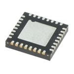
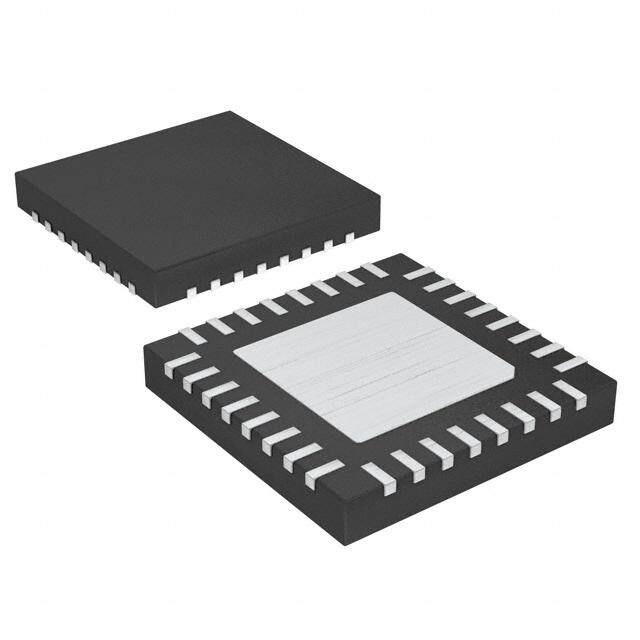
| 供应商器件封装 | 32-MLF®(5x5) |
| 其它名称 | 576-2101-5 |
| 功率耗散 | 260 mW |
| 包装 | 管件 |
| 商标 | Micrel |
| 安装类型 | 表面贴装 |
| 安装风格 | SMD/SMT |
| 封装 | Tray |
| 封装/外壳 | 32-VFQFN 裸露焊盘,32-MLF® |
| 封装/箱体 | QFN-32 |
| 工作温度 | -40°C ~ 85°C |
| 工厂包装数量 | 60 |
| 最大工作温度 | + 85 C |
| 最小工作温度 | - 40 C |
| 标准包装 | 60 |
| 独立电路 | 1 |
| 电压-电源 | 2.375 V ~ 2.625 V,3 V ~ 3.6 V |
| 电压源 | 单电源 |
| 电流-输出高,低 | - |
| 电源电压-最大 | 3.6 V |
| 电源电压-最小 | 2.375 V |
| 电路 | 1 x 4:1 |
| 类型 | 多路复用器 |
| 系列 | SY89855U |


- 商务部:美国ITC正式对集成电路等产品启动337调查
- 曝三星4nm工艺存在良率问题 高通将骁龙8 Gen1或转产台积电
- 太阳诱电将投资9.5亿元在常州建新厂生产MLCC 预计2023年完工
- 英特尔发布欧洲新工厂建设计划 深化IDM 2.0 战略
- 台积电先进制程称霸业界 有大客户加持明年业绩稳了
- 达到5530亿美元!SIA预计今年全球半导体销售额将创下新高
- 英特尔拟将自动驾驶子公司Mobileye上市 估值或超500亿美元
- 三星加码芯片和SET,合并消费电子和移动部门,撤换高东真等 CEO
- 三星电子宣布重大人事变动 还合并消费电子和移动部门
- 海关总署:前11个月进口集成电路产品价值2.52万亿元 增长14.8%


PDF Datasheet 数据手册内容提取
SY89855U Precision Low Power Differential LVPECL 4:1 MUX with 1:2 Fanout and Internal Termination General Description The SY89855U is a 2.5V/3.3V precision, high-speed, ® Precision Edge 4:1 differential multiplexer with 100K LVPECL (800mV) Features compatible outputs, capable of handling clocks up to 2.5GHz and data streams up to 2.5Gbps. In addition, a • Select 1 of 4 differential inputs 1:2 fanout buffer provides two copies of the selected • Provides two copies of the selected input inputs. • Low power 260mW (V = 2.5V) CC The differential input includes Micrel’s unique, 3-pin • Guaranteed AC performance over temperature and input termination architecture that allows customers to voltage: interface to any differential signal (AC- or DC-coupled) – DC-to->2.5Gbps data rate throughput as small as 100mV without any level shifting or – <410ps In-to-Q t termination resistor networks in the signal path. The pd result is a clean, stub-free, low-jitter interface solution. – <180ps tr / tf times The outputs are 800mV LVPECL, (100K temperature • Ultra low-jitter design: compensated) with fast rise/fall times guaranteed to be – <10ps total jitter (clock) PP less than 180ps. – <1ps random jitter RMS The SY89855U operates from a 2.5V ±5% supply or a – <10ps deterministic jitter PP 3.3V ±10% supply and is guaranteed over the full – <0.7ps crosstalk-induced jitter RMS industrial temperature range of –40°C to +85°C. For • Unique, patent-pending input design minimizes applications that require higher performance, consider crosstalk the SY58029U. The SY89855U is part of Micrel’s high- speed, Precision Edge® product line. • Accepts an input signal as low as 100mV • Unique patented input termination and VT pin All support documentation can be found on Micrel’s web accepts DC- and AC-coupled inputs (CML, LVPECL, site at www.micrel.com. LVDS) Typical Performance • 800mV 100K LVPECL output swing • Power supply 2.5V ±5% or 3.3V ±10% • –40°C to +85°C temperature range • Available in 32-pin (5mm x 5mm) QFN package Applications • Redundant clock and/or data distribution • All SONET/OC-3 to OC-48 clock/data distribution • Loopback • All Fibre Channel applications • All GigE applications Markets • LAN/WAN communication • Enterprise servers • ATE • Test and measurement Precision Edge is a registered trademark of Micrel, Inc. Micrel Inc. • 2180 Fortune Drive • San Jose, CA 95131 • USA • tel +1 (408) 944-0800 • fax + 1 (408) 474-1000 • http://www.micrel.com August 2007 M9999-082907-C hbwhelp@micrel.com or (408) 955-1690
Micrel, Inc. SY89855U Functional Block Diagram Truth Table SEL1 SEL0 Q 0 0 IN0 Input Select 0 1 IN1 Input Select 1 0 IN2 Input Select 1 1 IN3 Input Select August 2007 2 M9999-082907-C hbwhelp@micrel.com or (408) 955-1690
Micrel, Inc. SY89855U Ordering Information(1) Part Number Package Operating Package Marking Lead Finish Type Range SY89855UMG QFN-32 Industrial SY89855U with Pb-Free bar-line indicator NiPdAu Pb-Free SY89855UMGTR(2) QFN-32 Industrial SY89855U with Pb-Free bar-line indicator NiPdAu Pb-Free Notes: 1. Contact factory for die availability. Dice are guaranteed at T = 25ºC, DC Electricals only. A 2. Tape and Reel. Pin Configuration 32-Pin QFN Pin Description Pin Number Pin Name Pin Function 1, 4 IN0, /IN0, Differential Input: Each pair accepts AC- or DC-coupled signals as small as 100mV. Each 5, 8 IN1, /IN1, pin of a pair internally terminates to a VT pin through 50Ω. Note that these inputs will 25, 28 IN2, /IN2, default to an indeterminate state if left open. If an input is not used, connect one end of the 29, 32 IN3, /IN3 differential pairs to ground through a 1kΩ resistor, and leave the other end to VCC through an 825Ω resistor. Unused VT and VREF-AC pins may also be left floating. Please refer to the “Input Interface Applications” section for more details. 2, 6 VT0, VT1 Input Termination Center-Tap: Each side of the differential input pair terminates to a VT 26, 30 VT2, VT3 pin. The VT pin provides a center-tap to the termination network for maximum interface flexibility. See “Input Interface Applications” section for more details. 15, 18 SEL0, SEL1 This Single-Ended TTL/CMOS compatible input selects the inputs to the multiplexer. Note that this input is internally connected to a 25kΩ pull-up resistor and will default to a logic HIGH state if left open. Input logic threshold is V /2. See “Truth Table” for select control. CC 14, 19 NC Not connected. 10, 13, 16 VCC Positive Power Supply: Bypass with 0.1µF||0.01µF low ESR capacitors placed as close as 17, 20, 23 possible to each VCC pin. 11, 12 /Q0, Q0 Differential Outputs: These 100K-compatible (internally temperature compensated) 21, 22 /Q1, Q1 LVPECL output pairs are copies of the selected input. Unused output pins may be left floating. See “Output Interface” for terminating guidelines. 9, 24 GND, Ground: Ground pins and exposed pad must be connected to the most negative potential Exposed Pad of the chip. 3 VREF-AC0, Reference Voltage: This reference output is equivalent to V –1.2V. It is used for AC- CC 7 VREF-AC1, coupled inputs. When interfacing to AC input signals, connect VREF-AC directly to the VT 27 VREF-AC2, pin and bypass with a 0.01µF low ESR capacitor to VCC. See “Input Interface 31 VREF-AC3 Applications” section. Maximum sink/source current is ± 1.5mA. August 2007 3 M9999-082907-C hbwhelp@micrel.com or (408) 955-1690
Micrel, Inc. SY89855U Absolute Maximum Ratings(1) Operating Ratings(2) Supply Voltage (V )............................–0.5V to +4.0V Supply Voltage (V ).....................+2.375V to +2.625V CC CC Input Voltage (V )....................................–0.5V to V .....................................................+3.0V to +3.6V IN CC LVPECL Output Current (I ) Ambient Temperature (T )....................–40°C to +85°C OUT A Continuous.................................................±50mA Package Thermal Resistance(3) Surge.......................................................±100mA QFN (θ ) JA Termination Current Still-Air......................................................35°C/W Source or Sink Current on V ..................±100mA 500lfpm....................................................28°C/W T Input Current QFN (ψ ) JB Source or Sink Current on IN, /IN..............±50mA Junction-to-Board.....................................16°C/W Current (VREF-AC) Source or Sink Current on VREF-AC...............±2mA Lead Temperature (soldering, 20sec.)...............260°C Storage Temperature (Ts)................–65°C to +150°C DC Electrical Characteristics(4) T = –40°C to +85°C, unless otherwise noted. A Symbol Parameter Condition Min Typ Max Units V Power Supply Voltage V = 2.5V 2.375 2.5 2.625 V CC CC V = 3.3V 3.0 3.3 3.6 V CC I Power Supply Current No load, max. V . 65 85 mA CC CC R Input Resistance 45 50 55 Ω IN (IN-to-VT) R Differential Input Resistance 90 100 110 Ω DIFF_IN (IN-to-/IN, /IN-to-V ) T V Input High Voltage Note 5 V – 1.6 V V IH CC CC (IN, /IN) V Input Low Voltage 0 V – 0.1 V IL IH (IN, /IN) V Input Voltage Swing See Figure 1a. 0.1 1.7 V IN (IN-to-/IN) V Differential Input Voltage Swing See Figure 1b. 0.2 V DIFF_IN |IN- /IN| V Maximum Input Voltage 1.28 V T_IN (IN-to-V ) T V Output Reference Voltage V – 1.3 V – 1.2 V – 1.1 V REF-AC CC CC CC Notes: 1. Permanent device damage may occur if absolute maximum ratings are exceeded. This is a stress rating only and functional operation is not implied at conditions other than those detailed in the operational sections of this data sheet. Exposure to absolute maximum ratings conditions for extended periods may affect device reliability. 2. The data sheet limits are not guaranteed if the device is operated beyond the operating ratings. 3. Package thermal resistance assumes exposed pad is soldered (or equivalent) to the devices most negative potential on the PCB. θ and ψ JA JB values are determined for a 4-layer board in still-air, unless otherwise stated. 4. The circuit is designed to meet the DC specifications shown in the above table after thermal equilibrium has been established. 5. V (min) not lower than 1.2V. IH August 2007 4 M9999-082907-C hbwhelp@micrel.com or (408) 955-1690
Micrel, Inc. SY89855U LVPECL Output DC Electrical Characteristics(5) V = 2.5V ±5% or 3.3V ±10%; R = 50Ω to V –2V; T = –40°C to +85°C, unless otherwise noted. CC L CC A Symbol Parameter Condition Min Typ Max Units V Output High Voltage V –1.145 V –0.895 V OH CC CC (Q, /Q) V Output Low Voltage V –1.945 V –1.695 V OL CC CC (Q, /Q) V Output Voltage Swing See Figure 1a. 400 800 mV OUT (Q, /Q) V Differential Output Voltage Swing See Figure 1b. 800 1600 mV DIFF-OUT (Q, /Q) LVTTL/CMOS DC Electrical Characteristics(5) V = 2.5V ±5% or 3.3V ±10%; T = –40°C to +85°C, unless otherwise noted. CC A Symbol Parameter Condition Min Typ Max Units V Input High Voltage 2.0 V IH V Input Low Voltage 0.8 V IL I Input High Current V = V 75 µA IH IN CC I Input Low Current V = 0.5V –300 µA IL IN Notes: 5. The circuit is designed to meet the DC specifications shown in the above table after thermal equilibrium has been established. August 2007 5 M9999-082907-C hbwhelp@micrel.com or (408) 955-1690
Micrel, Inc. SY89855U AC Electrical Characteristics(6) V = 2.5V ±5% or 3.3V ±10%; T = –40°C to + 85°C, R = 50Ω to V –2V, unless otherwise stated. CC A L CC Symbol Parameter Condition Min Typ Max Units f Maximum Operating Frequency NRZ Data 2.5 Gbps MAX Clock, V > 400mV 2.5 GHz OUT t Propagation Delay pd IN-to-Q V > 100mV 210 300 410 ps IN SEL-to-Q 100 300 500 ps t Differential Propagation Delay 234 fs/°C pd Tempco Temperature Coefficient t Output-to-Output Note 7 9 20 ps SKEW Part-to-Part Note 8 150 ps t Data JITTER Random Jitter (RJ) Note 9 1 ps RMS Deterministic Jitter (DJ) Note 10 10 ps PP Clock Cycle-to-Cycle Jitter Note 11 1 ps RMS Total Jitter (TJ) Note 12 10 ps PP Crosstalk-induced Jitter Note 13 0.7 ps RMS (Adjacent Channel) t t Output Rise/Fall Time (20% to 80%) At full output swing. 50 100 180 ps r, f Notes: 6. High frequency AC electricals are guaranteed by design and characterization. 7. Output-to-output skew is measured between outputs under identical input conditions. 8. Part-to-part skew is defined for two parts with identical power supply voltages at the same temperature and with no skew of the edges at the respective inputs. 9. Random jitter is measured with a K28.7 character pattern, measured at <f . MAX 10. Deterministic jitter is measured at 2.5Gbps with both K28.5 and 223-1 PRBS pattern. 11. Cycle-to-cycle jitter definition: the variation of periods between adjacent cycles, T – T where T is the time between rising edges of the n n-1 output signal. 12. Total jitter definition: with an ideal clock input of frequency <f , no more than one output edge in 1012 output edges will deviate by more than MAX the specified peak-to-peak jitter value. 13. Crosstalk is measured at the output while applying two similar differential clock frequencies that are asynchronous with respect to each other at the inputs. August 2007 6 M9999-082907-C hbwhelp@micrel.com or (408) 955-1690
Micrel, Inc. SY89855U Typical Operating Characteristics V = 2.5V, GND = 0, V = 100mV; T = –40°C to + 85°C, R = 50Ω to V –2V, unless otherwise stated. CC IN A L CC August 2007 7 M9999-082907-C hbwhelp@micrel.com or (408) 955-1690
Micrel, Inc. SY89855U Functional Characteristics V = 3.3V ±10%; T = –40°C to + 85°C, R = 50Ω to V –2V, unless otherwise stated. CC A L CC August 2007 8 M9999-082907-C hbwhelp@micrel.com or (408) 955-1690
Micrel, Inc. SY89855U Single-Ended and Differential Swings Figure 1a. Single-Ended Voltage Swing Figure 1b. Differential Voltage Swing Timing Diagram IN-to-Q Timing Diagram SEL-to-Q Timing Diagram August 2007 9 M9999-082907-C hbwhelp@micrel.com or (408) 955-1690
Micrel, Inc. SY89855U Input and Output Stages Figure 2a. Simplified Differential Input Stage Figure 2b. PECL Output Stage Input Interface Applications option: may connect VT to V CC Figure 3a. LVPECL Interface Figure 3b. LVPECL Interface Figure 3c. CML Interface (DC-Coupled) (AC-Coupled) (DC-Coupled) Figure 3d. CML Interface Figure 3e. LVDS Interface (AC-Coupled) August 2007 10 M9999-082907-C hbwhelp@micrel.com or (408) 955-1690
Micrel, Inc. SY89855U Output Interface Applications LVPECL outputs: parallel termination thevenin- equivalent, parallel termination (3-resistor), and AC- LVPECL has high input impedance, very low output coupled termination. Unused output pairs may be left (open emitter) impedance, and small signal swing, floating; however, single-ended outputs must be which result in low EMI. LVPECL is ideal for driving terminated or balanced. 50Ω and 100Ω controlled impedance transmission lines. There are different techniques for terminating Note: Note: For a 2.5V system, R1 = 250Ω, R2 = 62.5Ω. 1. For a 2.5V system, Rb = 19Ω. Figure 4a. Parallel Thevenin-Equivalent Figure 4b. Parallel Termination Termination (3-Resistor) Note: Note: For a 2.5V system, R = 50Ω. For a 2.5V system, R1 = 250Ω, R2 = 62.5 Ω. Figure 4c. AC-Coupled Termination Figure 4d. Parallel Thevenin-Equivalent Termination Related Product and Support Documentation Part Number Function Data Sheet Link SY58029U Ultra Precision Differential LVPECL 4 :1 www.micrel.com/product-info/products/sy58029u.shtml. MUX with 1 :2 Fanout Internal Termination HBW Solutions New Products and Applications www.micrel.com/product-info/products/solutions.shtml August 2007 11 M9999-082907-C hbwhelp@micrel.com or (408) 955-1690
Micrel, Inc. SY89855U Package Information 32-Pin QFN PCB Thermal Consideration for 32-Pin QFN Package (Always solder, or equivalent, the exposed pad to the PCB) Packages Notes: 1. Package meets Level 2 Moisture Sensitivity Classification. 2. All parts are dry-packed before shipment. 3. Exposed pads must be soldered to a ground for proper thermal management. August 2007 12 M9999-082907-C hbwhelp@micrel.com or (408) 955-1690
Micrel, Inc. SY89855U MICREL, INC. 2180 FORTUNE DRIVE SAN JOSE, CA 95131 USA TEL +1 (408) 944-0800 FAX +1 (408) 474-1000 WEB http:/www.micrel.com The information furnished by Micrel in this data sheet is believed to be accurate and reliable. However, no responsibility is assumed by Micrel for its use. Micrel reserves the right to change circuitry and specifications at any time without notification to the customer. Micrel Products are not designed or authorized for use as components in life support appliances, devices or systems where malfunction of a product can reasonably be expected to result in personal injury. Life support devices or systems are devices or systems that (a) are intended for surgical implant into the body or (b) support or sustain life, and whose failure to perform can be reasonably expected to result in a significant injury to the user. A Purchaser’s use or sale of Micrel Products for use in life support appliances, devices or systems is a Purchaser’s own risk and Purchaser agrees to fully indemnify Micrel for any damages resulting from such use or sale. © 2005 Micrel, Incorporated. August 2007 13 M9999-082907-C hbwhelp@micrel.com or (408) 955-1690
Mouser Electronics Authorized Distributor Click to View Pricing, Inventory, Delivery & Lifecycle Information: M icrochip: SY89855UMG SY89855UMG-TR