ICGOO在线商城 > 集成电路(IC) > 逻辑 - 缓冲器,驱动器,接收器,收发器 > SN74AHCT245PW
 Datasheet下载
- 型号: SN74AHCT245PW
- 制造商: Texas Instruments
- 库位|库存: xxxx|xxxx
- 要求:
| 数量阶梯 | 香港交货 | 国内含税 |
| +xxxx | $xxxx | ¥xxxx |
查看当月历史价格
查看今年历史价格
SN74AHCT245PW产品简介:
ICGOO电子元器件商城为您提供SN74AHCT245PW由Texas Instruments设计生产,在icgoo商城现货销售,并且可以通过原厂、代理商等渠道进行代购。 SN74AHCT245PW价格参考¥2.85-¥8.18。Texas InstrumentsSN74AHCT245PW封装/规格:逻辑 - 缓冲器,驱动器,接收器,收发器, Transceiver, Non-Inverting 1 Element 8 Bit per Element 3-State Output 20-TSSOP。您可以下载SN74AHCT245PW参考资料、Datasheet数据手册功能说明书,资料中有SN74AHCT245PW 详细功能的应用电路图电压和使用方法及教程。
SN74AHCT245PW 是由 Texas Instruments 生产的一款逻辑缓冲器、驱动器、接收器和收发器。它属于 8 位双向电压电平转换器,能够在不同的电压域之间进行数据传输,广泛应用于各种数字电路设计中。

 应用场景:

1. 总线扩展与隔离:
   SN74AHCT245PW 可用于扩展数据总线的宽度或在不同子系统之间提供电气隔离。例如,在多处理器系统或多总线架构中,它可以确保信号的完整性和防止干扰。

2. 电压电平转换:
   该器件支持不同的电源电压(VCC)范围(2V 至 6V),因此可以在低电压和高电压系统之间进行无缝通信。例如,在一个混合信号系统中,前端使用 3.3V 逻辑电平,而后端需要 5V 逻辑电平,SN74AHCT245PW 可以在这两者之间进行转换。

3. 数据传输与同步:
   在需要高速数据传输的应用中,如工业控制、通信设备和消费电子,SN74AHCT245PW 可以确保数据的可靠传输。其双向特性允许在同一总线上实现数据的发送和接收,减少了所需的引脚数量和布线复杂度。

4. 存储器接口:
   该器件常用于连接存储器模块和其他外设。例如,在嵌入式系统中,它可以作为存储器控制器和外部 RAM 或 ROM 之间的桥梁,确保数据的正确读写操作。

5. I/O 扩展:
   在 I/O 端口有限的微控制器或 FPGA 系统中,SN74AHCT245PW 可以扩展可用的 I/O 引脚数量。通过级联多个器件,可以实现更多的输入输出通道。

6. 测试与调试工具:
   在开发过程中,工程师可以利用 SN74AHCT245PW 来监控和控制信号流,帮助诊断和解决硬件问题。其双向特性和低功耗特性使其成为理想的调试工具。

总之,SN74AHCT245PW 凭借其双向传输能力、宽电压范围和低功耗特性,适用于多种应用场景,特别是在需要跨电压域通信和总线扩展的场合。
| 参数 | 数值 |
| 产品目录 | 集成电路 (IC)半导体 |
| 描述 | IC BUS TRANSCEIVER 8BIT 20TSSOP总线收发器 Octal Transparent |
| 产品分类 | |
| 品牌 | Texas Instruments |
| 产品手册 | |
| 产品图片 |
|
| rohs | 符合RoHS无铅 / 符合限制有害物质指令(RoHS)规范要求 |
| 产品系列 | 逻辑集成电路,总线收发器,Texas Instruments SN74AHCT245PW74AHCT |
| 数据手册 | |
| 产品型号 | SN74AHCT245PW |
| 产品种类 | 总线收发器 |
| 传播延迟时间 | 9.5 ns |
| 低电平输出电流 | 8 mA |
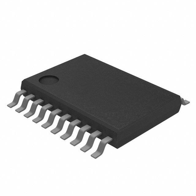
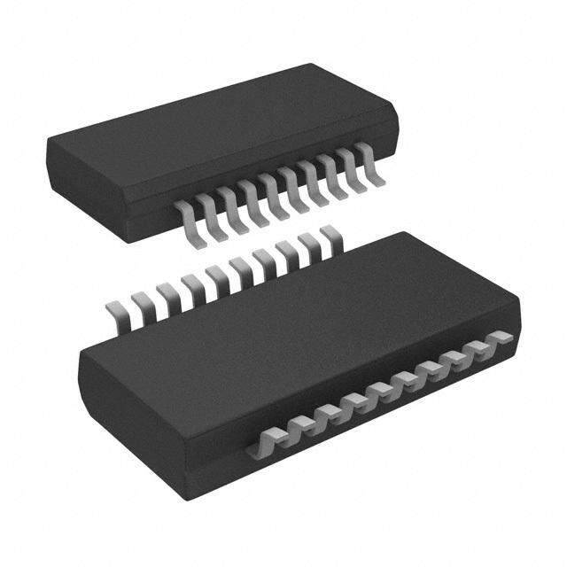
| 供应商器件封装 | 20-TSSOP |
| 元件数 | 1 |
| 其它名称 | 296-26420-5 |
| 功能 | Octal Transparent |
| 包装 | 管件 |
| 单位重量 | 77 mg |
| 商标 | Texas Instruments |
| 安装类型 | 表面贴装 |
| 安装风格 | SMD/SMT |
| 封装 | Tube |
| 封装/外壳 | 20-TSSOP(0.173",4.40mm 宽) |
| 封装/箱体 | TSSOP-20 |
| 工作温度 | -40°C ~ 125°C |
| 工厂包装数量 | 70 |
| 最大工作温度 | + 85 C |
| 最小工作温度 | - 40 C |
| 极性 | Non-Inverting |
| 标准包装 | 70 |
| 每元件位数 | 8 |
| 每芯片的通道数量 | 8 |
| 电压-电源 | 4.5 V ~ 5.5 V |
| 电流-输出高,低 | 8mA,8mA |
| 电源电压-最大 | 5.5 V |
| 电源电压-最小 | 4.5 V |
| 电路数量 | 8 |
| 系列 | SN74AHCT245 |
| 输入电平 | TTL |
| 输出电平 | CMOS |
| 输出类型 | 3-State |
| 逻辑类型 | Standard Transceiver |
| 逻辑系列 | AHCT |
| 高电平输出电流 | - 8 mA |


- 商务部:美国ITC正式对集成电路等产品启动337调查
- 曝三星4nm工艺存在良率问题 高通将骁龙8 Gen1或转产台积电
- 太阳诱电将投资9.5亿元在常州建新厂生产MLCC 预计2023年完工
- 英特尔发布欧洲新工厂建设计划 深化IDM 2.0 战略
- 台积电先进制程称霸业界 有大客户加持明年业绩稳了
- 达到5530亿美元!SIA预计今年全球半导体销售额将创下新高
- 英特尔拟将自动驾驶子公司Mobileye上市 估值或超500亿美元
- 三星加码芯片和SET,合并消费电子和移动部门,撤换高东真等 CEO
- 三星电子宣布重大人事变动 还合并消费电子和移动部门
- 海关总署:前11个月进口集成电路产品价值2.52万亿元 增长14.8%


PDF Datasheet 数据手册内容提取
Product Sample & Technical Tools & Support & Folder Buy Documents Software Community SN54AHCT245,SN74AHCT245 SCLS233P–OCTOBER1995–REVISEDJULY2014 SNx4AHCT245 Octal Bus Transceivers With 3-State Outputs 1 Features 3 Description • InputsAreTTL-VoltageCompatible The SNx4AHCT245 octal bus transceivers are 1 designed for asynchronous two-way communication • Latch-UpPerformanceExceeds250mAPer between data buses. These parts operate from 4.5 V JESD17 to5.5V. • ESDProtectionExceedsJESD22 – 2000-VHuman-BodyModel(A114-A) DeviceInformation(1) – 200-VMachineModel(A115-A) PARTNUMBER PACKAGE BODYSIZE(NOM) PDIP(20) 25.40x6.35mm – 1000-VCharged-DeviceModel(C101) SOP(20) 12.60x5.30mm • OnProductsComplianttoMIL-PRF-38535, SNx4AHCT245 SSOP(20) 7.50x5.30mm AllParametersAreTestedUnlessOtherwise Noted.OnAllOtherProducts,Production TVSOP(20) 5.00x4.40mm ProcessingDoesNotNecessarilyIncludeTesting SOIC(20) 12.80x7.50mm ofAllParameters. (1) For all available packages, see the orderable addendum at theendofthedatasheet. 2 Applications • Servers • PCsandNotebooks • NetworkSwitches • WearableHealthandFitnessDevices • TelecomInfrastructures • ElectronicPointsofSale 4 Simplified Schematic 1 DIR 19 OE 2 A1 18 B1 To Seven Other Channels 1 An IMPORTANT NOTICE at the end of this data sheet addresses availability, warranty, changes, use in safety-critical applications, intellectualpropertymattersandotherimportantdisclaimers.PRODUCTIONDATA.
SN54AHCT245,SN74AHCT245 SCLS233P–OCTOBER1995–REVISEDJULY2014 www.ti.com Table of Contents 1 Features.................................................................. 1 9.1 Overview...................................................................8 2 Applications........................................................... 1 9.2 FunctionalBlockDiagram.........................................8 3 Description............................................................. 1 9.3 FeatureDescription...................................................8 9.4 DeviceFunctionalModes..........................................8 4 SimplifiedSchematic............................................. 1 10 ApplicationandImplementation.......................... 9 5 RevisionHistory..................................................... 2 10.1 ApplicationInformation............................................9 6 PinConfigurationandFunctions......................... 3 10.2 TypicalApplication..................................................9 7 Specifications......................................................... 4 11 PowerSupplyRecommendations..................... 10 7.1 AbsoluteMaximumRatings......................................4 12 Layout................................................................... 10 7.2 HandlingRatings.......................................................4 12.1 LayoutGuidelines.................................................10 7.3 RecommendedOperatingConditions.......................4 12.2 LayoutExample....................................................10 7.4 ThermalInformation..................................................5 13 DeviceandDocumentationSupport................. 11 7.5 ElectricalCharacteristics...........................................5 7.6 SwitchingCharacteristics.........................................6 13.1 RelatedLinks........................................................11 7.7 NoiseCharacteristics................................................6 13.2 Trademarks...........................................................11 7.8 OperatingCharacteristics........................................6 13.3 ElectrostaticDischargeCaution............................11 7.9 TypicalCharacteristics..............................................6 13.4 Glossary................................................................11 8 ParameterMeasurementInformation..................7 14 Mechanical,Packaging,andOrderable Information........................................................... 11 9 DetailedDescription.............................................. 8 5 Revision History NOTE:Pagenumbersforpreviousrevisionsmaydifferfrompagenumbersinthecurrentversion. ChangesfromRevisionO(August2013)toRevisionP Page • UpdateddocumenttonewTIdatasheetformat.................................................................................................................... 1 • AddedMilitaryDisclaimertoFeatureslist. ............................................................................................................................ 1 • AddedApplications................................................................................................................................................................. 1 • AddedPinFunctionstable..................................................................................................................................................... 3 • AddedHandlingRatingstable................................................................................................................................................ 4 • AddedThermalInformationtable........................................................................................................................................... 5 • AddedTypicalCharacteristics................................................................................................................................................ 6 • AddedDetailedDescriptionsection........................................................................................................................................ 8 • AddedApplicationandImplementationsection...................................................................................................................... 9 ChangesfromRevisionN(March2005)toRevisionO Page • RemovedOrderingInformationtable..................................................................................................................................... 1 • Extendedoperatingtemperaturerangeto125°C................................................................................................................... 4 2 SubmitDocumentationFeedback Copyright©1995–2014,TexasInstrumentsIncorporated ProductFolderLinks:SN54AHCT245 SN74AHCT245
SN54AHCT245,SN74AHCT245 www.ti.com SCLS233P–OCTOBER1995–REVISEDJULY2014 6 Pin Configuration and Functions SN54AHCT245 . . . J OR W PACKAGE SN74AHCT245...RGYPACKAGE SN54AHCT245...FKPACKAGE SN74AHCT245...DB,DGV,DW,N,NS, (TOPVIEW) (TOPVIEW) ORPWPACKAGE (TOPVIEW) DIR VCC A2 A1 DIRVCCOE DIR 1 20 VCC 1 20 3 2 1 20 19 A1 2 19 OE A1 2 19 OE A3 4 18 B1 A2 3 18 B1 A2 3 18 B1 A4 5 17 B2 A3 4 17 B2 A3 4 17 B2 A5 6 16 B3 A4 5 16 B3 A4 5 16 B3 A6 7 15 B4 A5 6 15 B4 A5 6 15 B4 A7 89 10 11 12 1314 B5 A6 7 14 B5 A6 7 14 B5 A7 8 13 B6 A7 8 13 B6 8 D 87 6 A8 9 12 B7 A N BB B A8 9 12 B7 G GND 10 11 B8 10 11 D 8 N B G PinFunctions PIN I/O DESCRIPTION NO. NAME 1 DIR — DirectionPin 2 A1 I/O A1Input/Output 3 A2 I/O A2Input/Output 4 A3 I/O A3Input/Output 5 A4 I/O A4Input/Output 6 A5 I/O A5Input/Output 7 A6 I/O A6Input/Output 8 A7 I/O A7Input/Output 9 A8 I/O A8Input/Output 10 GND — GroundPin 11 B8 I/O B8Input/Output 12 B7 I/O B7Input/Output 13 B6 I/O B6Input/Output 14 B5 I/O B5Input/Output 15 B4 I/O B4Input/Output 16 B3 I/O B3Input/Output 17 B2 I/O B2Input/Output 18 B1 I/O B1Input/Output 19 OE I OutputEnable 20 VCC — PowerPin Copyright©1995–2014,TexasInstrumentsIncorporated SubmitDocumentationFeedback 3 ProductFolderLinks:SN54AHCT245 SN74AHCT245
SN54AHCT245,SN74AHCT245 SCLS233P–OCTOBER1995–REVISEDJULY2014 www.ti.com 7 Specifications 7.1 Absolute Maximum Ratings overoperatingfree-airtemperaturerange(unlessotherwisenoted)(1) MIN MAX UNIT V Supplyvoltagerange –0.5 7 V CC V Inputvoltagerange(2) Controlinputs –0.5 7 V I V Outputvoltagerange(2) –0.5 V +0.5 V O CC I Inputclampcurrent V <0 Controlinputs –20 mA IK I I Outputclampcurrent V <0orV >V ±20 mA OK O O CC I Continuousoutputcurrent V =0toV ±25 mA O O CC ContinuouscurrentthroughV orGND ±75 mA CC (1) StressesbeyondthoselistedunderAbsoluteMaximumRatingsmaycausepermanentdamagetothedevice.Thesearestressratings only,andfunctionaloperationofthedeviceattheseoranyotherconditionsbeyondthoseindicatedunderRecommendedOperating Conditionsisnotimplied.Exposuretoabsolute-maximum-ratedconditionsforextendedperiodsmayaffectdevicereliability. (2) Theinputandoutputvoltageratingsmaybeexceedediftheinputandoutputcurrentratingsareobserved. 7.2 Handling Ratings MIN MAX UNIT T Storagetemperaturerange –65 150 °C stg Humanbodymodel(HBM),perANSI/ESDA/JEDECJS-001,all pins(1) 0 2000 V Electrostaticdischarge V (ESD) Chargeddevicemodel(CDM),perJEDECspecification JESD22-C101,allpins(2) 0 1000 (1) JEDECdocumentJEP155statesthat500-VHBMallowssafemanufacturingwithastandardESDcontrolprocess. (2) JEDECdocumentJEP157statesthat250-VCDMallowssafemanufacturingwithastandardESDcontrolprocess. 7.3 Recommended Operating Conditions overoperatingfree-airtemperaturerange(unlessotherwisenoted)(1) SN54AHCT245 SN74AHCT245 UNIT MIN MAX MIN MAX V Supplyvoltage 4.5 5.5 4.5 5.5 V CC V High-levelinputvoltage 2 2 V IH V Low-levelInputvoltage 0.8 0.8 V IL V Inputvoltage 0 5.5 0 5.5 V I V Outputvoltage 0 V 0 V V O CC CC I High-leveloutputcurrent –8 –8 mA OH I Low-leveloutputcurrent 8 8 mA OL Δt/Δv InputTransitionriseandfallrate 20 20 ns/V T Operatingfree-airtemperature –55 125 –40 125 °C A (1) AllunusedinputsofthedevicemustbeheldatV orGNDtoensureproperdeviceoperation.RefertotheTIapplicationreport, CC ImplicationsofSloworFloatingCMOSInputs,literaturenumberSCBA004. 4 SubmitDocumentationFeedback Copyright©1995–2014,TexasInstrumentsIncorporated ProductFolderLinks:SN54AHCT245 SN74AHCT245
SN54AHCT245,SN74AHCT245 www.ti.com SCLS233P–OCTOBER1995–REVISEDJULY2014 7.4 Thermal Information SN74AHCT245 THERMALMETRIC(1) DB DGV DW N NS PW RGY UNIT 20PINS Junction-to-ambientthermal RθJA resistance 96.0 116.1 79.8 51.5 77.1 102.8 35.1 Junction-to-case(top)thermal RθJC(top) resistance 57.7 31.3 45.8 38.2 43.6 36.8 43.3 RθJB Junction-to-boardthermalresistance 51.2 57.6 47.4 32.4 44.6 53.8 12.9 Junction-to-topcharacterization °C/W ψJT parameter 19.4 1.0 18.5 24.6 17.2 2.5 0.9 Junction-to-boardcharacterization ψJB parameter 50.8 56.9 47.0 32.3 44.2 53.3 12.9 Junction-to-case(bottom)thermal RθJC(bot) resistance n/a n/a n/a n/a n/a n/a 7.9 (1) Formoreinformationabouttraditionalandnewthermalmetrics,seetheICPackageThermalMetricsapplicationreport,SPRA953. 7.5 Electrical Characteristics overrecommendedoperatingfree-airtemperaturerange(unlessotherwisenoted) Recommended SN54AHCT245 SN74AHCT245 PARAMETER TESTCONDITIONS VCC TA=25°C –55°CTO125°C –40°CTO85°C –S4N0°7C4ATHOC1T2254°5C UNIT MIN TYP MAX MIN MAX MIN MAX MIN MAX IOH=–50µA 4.4 4.5 4.4 4.4 4.4 VOH 4.5V V IOH=–8mA 3.94 3.8 3.8 3.7 IOL=50µA 0.1 0.1 0.1 0.1 VOL 4.5V V IOH=8mA 0.36 0.44 0.44 0.44 II OEorDIR VI=5.5VorGND 50.5toV ±0.1 ±1(1) ±1 ±1 µA AorB IOZ inputs(2) VO=VCCorGND 5.5V ±.25 ±2.5 ±2.5 ±2.5 µA ICC VI=VCCorGND, IO=0 5.5V 4 40 40 40 µA ΔICC(3) OOntheerinipnuptuatsta3t.4VCVC,orGND 5.5V 1.35 1.5 1.5 1.5 mA Ci OEorDIR VI=VCCorGND 5V 2.5 10 10 pF AorB Cio inputs VI=VCCorGND 5V 4 pF (1) OnproductscomplianttoMIL-PRF-38535,thisparameterisnotproductiontestedatV =0V. CC (2) ForI/Oports,theparameterI includestheinputleakagecurrent. OZ (3) ThisistheincreaseinsupplycurrentforeachinputatoneofthespecifiedTTLvoltagelevels,ratherthan0VorV . CC Copyright©1995–2014,TexasInstrumentsIncorporated SubmitDocumentationFeedback 5 ProductFolderLinks:SN54AHCT245 SN74AHCT245
SN54AHCT245,SN74AHCT245 SCLS233P–OCTOBER1995–REVISEDJULY2014 www.ti.com 7.6 Switching Characteristics overrecommendedoperatingfree-airtemperaturerange,V =5V±0.5V(unlessotherwisenoted)(seeFigure2) CC Recommended SN54AHCT245 SN74AHCT245 PARAMETER (IFNRPOUMT) (OUTTOPUT) CAPALCOIATDANCE TA=25°C –55°CTO125°C –40°CTO85°C –S4N0°7C4ATHOC1T2254°5C UNIT TYP MAX MIN MAX MIN MAX MIN MAX tPLH 4.5(1) 7.7(1) 1(1) 10(1) 1 8.5 1 10 tPHL AorB BorA CL=15pF 4.5(1) 7.7(1) 1(1) 10(1) 1 8.5 1 10 ns tPZH 8.9(1) 13.8(1) 1(1) 16(1) 1 15 1 16 tPZL OE AorB CL=15pF 8.9(1) 13.8(1) 1(1) 16(1) 1 15 1 16 ns tPHZ 9.2(1) 14.4(1) 1(1) 16.5(1) 1 15.5 1 16.5 tPLZ OE AorB CL=15pF 9.2(1) 14.4(1) 1(1) 16.5(1) 1 15.5 1 16.5 ns tPLH 5.3 8.7 1 11 1 9.5 1 11 AorB BorA CL=50pF ns tPHL 5.3 8.7 1 11 1 9.5 1 11 tPZH 9.7 14.8 1 17 1 16 1 17 OE AorB CL=50pF ns tPZL 9.7 14.8 1 17 1 16 1 17 tPHZ 10 15.4 1 17.5 1 16.5 1 17.5 OE AorB CL=50pF ns tPLZ 10 15.4 1 17.5 1 16.5 1 17.5 tsk(o) CL=50pF 1(2) 1 ns (1) OnproductscomplianttoMIL-PRF-38535,thisparameterisnotproductiontested. (2) OnproductscomplianttoMIL-PRF-38535,thisparameterdoesnotapply. 7.7 Noise Characteristics V =5V,C =50pF,T =25°C(1) CC L A SN74AHCT245 PARAMETER UNIT MIN TYP MAX V Quietoutput,minimumdynamicV 4 V OH(V) OH V High-leveldynamicinputvoltage 2 V IH(D) V Low-leveldynamicinputvoltage 0.8 V IL(D) (1) Characteristicsareforsurface-mountpackagesonly. 7.8 Operating Characteristics V =5V,T =25°C CC A PARAMETER TESTCONDITIONS TYP UNIT C Powerdissipationcapacitance Noload, f=1MHz 13 pF pd 7.9 Typical Characteristics 7 6 5 s) 4 n D ( P 3 T 2 1 TPD in ns 0 -100 -50 0 50 100 150 Temperature (qC) D001 Figure1.SN74AHCT245TPDvsTemperature,15pFLoad 6 SubmitDocumentationFeedback Copyright©1995–2014,TexasInstrumentsIncorporated ProductFolderLinks:SN54AHCT245 SN74AHCT245
SN54AHCT245,SN74AHCT245 www.ti.com SCLS233P–OCTOBER1995–REVISEDJULY2014 8 Parameter Measurement Information VCC From Output Test From Output RL= 1 kΩ S1 Open TEST S1 UnderTest Point UnderTest GND tPLH/tPHL Open CL CL tPLZ/tPZL VCC (see NoteA) (see NoteA) tPHZ/tPZH GND Open Drain VCC LOAD CIRCUIT FOR LOAD CIRCUIT FOR TOTEM-POLE OUTPUTS 3-STATEAND OPEN-DRAIN OUTPUTS 3 V Timing Input 1.5 V tw 0 V th 3 V tsu 3 V Input 1.5 V 1.5 V Data Input 1.5 V 1.5 V 0 V 0 V VOLTAGEWAVEFORMS VOLTAGEWAVEFORMS PULSEDURATION SETUPAND HOLD TIMES 3 V 3 V Output Input 1.5 V 1.5 V 1.5 V 1.5 V Control 0 V 0 V tPLH tPHL tPZL tPLZ Output VOH Waveform 1 ≈VCC InO-Puhtapsuet 50%VCC 50% VCC S1 at VCC 50% VCC VOL+0.3V VOL (see Note B) VOL tPHL tPLH tPZH tPHZ Output Out-ofO-Puhtapsuet 50% VCC 50% VCVVCOOHL (WseSae1v eNaftoo GtremN B D2) 50% VCC VOH−0.3VV≈0O VH VOLTAGEWAVEFORMS VOLTAGEWAVEFORMS PROPAGATIONDELAYTIMES ENABLEAND DISABLE TIMES INVERTINGAND NONINVERTING OUTPUTS LOW-AND HIGH-LEVELENABLING A. C includesprobeandjigcapacitance. L B. Waveform1 is for an outputwith internalconditions such that theoutputis lowexceptwhendisabledby theoutput control. Waveform2isforanoutputwithinternalconditionssuchthattheoutputishighexceptwhendisabledbytheoutput control. C. Allinputpulsesaresuppliedbygeneratorshavingthefollowingcharacteristics:PRR≤1MHz,Z =50Ω,t ≤3ns, O r t ≤3ns. f D. Theoutputsaremeasuredoneatatimewithoneinputtransitionpermeasurement. E. Allparametersandwaveformsarenotapplicabletoalldevices. Figure2. LoadCircuitandVoltageWaveforms Copyright©1995–2014,TexasInstrumentsIncorporated SubmitDocumentationFeedback 7 ProductFolderLinks:SN54AHCT245 SN74AHCT245
SN54AHCT245,SN74AHCT245 SCLS233P–OCTOBER1995–REVISEDJULY2014 www.ti.com 9 Detailed Description 9.1 Overview TheSNx7ACHT245octalbustransceiversaredesignedforasynchronoustwo-waycommunicationbetweendata buses. The control-function implementation minimizes external timing requirements. The SNx4AHCT245 devices allow data transmission from the A bus to the B bus or from the B bus to the A bus, depending on the logic level at the direction– control (DIR) input. The output-enable (OE) input can be used to disable the device so that the buses effectively are isolated. To ensure the high-impedance state during power up or power down, OE should be tied to V through a pullup resistor; the minimum value of the resistor is determined by the current-sinking CC capabilityofthedriver. 9.2 Functional Block Diagram 1 DIR 19 OE 2 A1 18 B1 To Seven Other Channels Figure3. LogicDiagram(PositiveLogic) 9.3 Feature Description • V isoptimizedat5V CC • Allowsupvoltagetranslationfrom3.3Vto5V – InputsAcceptV levelsof2V IH • Slowedgeratesminimizeoutputringing 9.4 Device Functional Modes Table1.FunctionTable (EachTransceiver) INPUTS OPERATION OE DIR L L BdatatoAbus L H AdatatoBbus H X Isolation 8 SubmitDocumentationFeedback Copyright©1995–2014,TexasInstrumentsIncorporated ProductFolderLinks:SN54AHCT245 SN74AHCT245
SN54AHCT245,SN74AHCT245 www.ti.com SCLS233P–OCTOBER1995–REVISEDJULY2014 10 Application and Implementation 10.1 Application Information The SN74AHCT245 is a low drive CMOS device that can be used for a multitude of bus interface type applications where output ringing is a concern. The low drive and slow edge rates will minimize overshoot and undershoot on the outputs. The input switching levels have been lowered to accommodate TTL inputs of 0.8 V V and 2 V V . This feature makes it ideal for translating up from 3.3 V to 5 V. The figure below shows this type IL IH oftranslation. 10.2 Typical Application Regulated 5 V OE VCC DIR A1 B1 5 V LEDs, Relays, 3.3 V µC or other system boards A8 B8 GND Figure4. TypicalApplicationDiagram 10.2.1 DesignRequirements This device uses CMOS technology and has balanced output drive. Care should be taken to avoid bus contention because it can drive currents that would exceed maximum limits. The high drive will also create fast edgesintolightloadssoroutingandloadconditionsshouldbeconsideredtopreventringing. 10.2.2 DetailedDesignProcedure • Recommendedinputconditions – Specifiedhighandlowlevels.See(V andV )intheRecommendedOperatingConditions table. IH IL – Specifiedhighandlowlevels.See(V andV )intheRecommendedOperatingConditions table. IH IL – Inputsareovervoltagetolerantallowingthemtogoashighas5.5VatanyvalidV CC • Recommendoutputconditions – Loadcurrentsshouldnotexceed25mAperoutputand50mAtotalforthepart – OutputsshouldnotbepulledaboveV CC Copyright©1995–2014,TexasInstrumentsIncorporated SubmitDocumentationFeedback 9 ProductFolderLinks:SN54AHCT245 SN74AHCT245
SN54AHCT245,SN74AHCT245 SCLS233P–OCTOBER1995–REVISEDJULY2014 www.ti.com Typical Application (continued) 10.2.3 ApplicationCurves Output Input Figure5.TypicalApplicationCurve 11 Power Supply Recommendations The power supply can be any voltage between the MIN and MAX supply voltage rating located in the RecommendedOperatingConditionstable. Each VCC pin should have a good bypass capacitor to prevent power disturbance. For devices with a single supply, 0.1 μf is recommended; if there are multiple VCC pins, then 0.01 μf or 0.022 μf is recommended for each power pin. It is acceptable to parallel multiple bypass caps to reject different frequencies of noise. A 0.1 μf and a 1 μf are commonly used in parallel. The bypass capacitor should be installed as close to the power pin as possibleforbestresults. 12 Layout 12.1 Layout Guidelines Whenusingmultiple-bitlogicdevices,inputsshouldneverfloat. In many cases, functions or parts of functions of digital logic devices are unused, for example, when only two inputsofatriple-inputANDgateareusedoronly3ofthe4buffergatesareused.Suchinputpinsshouldnot be left unconnected because the undefined voltages at the outside connections result in undefined operational states. Figure 6 specifies the rules that must be observed under all circumstances. All unused inputs of digital logic devices must be connected to a high or low bias to prevent them from floating. The logic level that should be applied to any particular unused input depends on the function of the device. Generally they will be tied to GND or V , whichever makes more sense or is more convenient. It is CC generally acceptable to float outputs, unless the part is a transceiver. If the transceiver has an output enable pin, it will disable the output section of the part when asserted. This will not disable the input section of the I/Os,sotheycannotfloatwhendisabled. 12.2 Layout Example V cc Input Unused Input Output Unused Input Output Input Figure6. LayoutDiagram 10 SubmitDocumentationFeedback Copyright©1995–2014,TexasInstrumentsIncorporated ProductFolderLinks:SN54AHCT245 SN74AHCT245
SN54AHCT245,SN74AHCT245 www.ti.com SCLS233P–OCTOBER1995–REVISEDJULY2014 13 Device and Documentation Support 13.1 Related Links The table below lists quick access links. Categories include technical documents, support and community resources,toolsandsoftware,andquickaccesstosampleorbuy. Table2.RelatedLinks TECHNICAL TOOLS& SUPPORT& PARTS PRODUCTFOLDER SAMPLE&BUY DOCUMENTS SOFTWARE COMMUNITY SN54AHCT245 Clickhere Clickhere Clickhere Clickhere Clickhere SN74AHCT245 Clickhere Clickhere Clickhere Clickhere Clickhere 13.2 Trademarks Alltrademarksarethepropertyoftheirrespectiveowners. 13.3 Electrostatic Discharge Caution Thesedeviceshavelimitedbuilt-inESDprotection.Theleadsshouldbeshortedtogetherorthedeviceplacedinconductivefoam duringstorageorhandlingtopreventelectrostaticdamagetotheMOSgates. 13.4 Glossary SLYZ022—TIGlossary. Thisglossarylistsandexplainsterms,acronyms,anddefinitions. 14 Mechanical, Packaging, and Orderable Information The following pages include mechanical, packaging, and orderable information. This information is the most current data available for the designated devices. This data is subject to change without notice and revision of thisdocument.Forbrowser-basedversionsofthisdatasheet,refertotheleft-handnavigation. Copyright©1995–2014,TexasInstrumentsIncorporated SubmitDocumentationFeedback 11 ProductFolderLinks:SN54AHCT245 SN74AHCT245
PACKAGE OPTION ADDENDUM www.ti.com 6-Feb-2020 PACKAGING INFORMATION Orderable Device Status Package Type Package Pins Package Eco Plan Lead/Ball Finish MSL Peak Temp Op Temp (°C) Device Marking Samples (1) Drawing Qty (2) (6) (3) (4/5) 5962-9681901Q2A ACTIVE LCCC FK 20 1 TBD POST-PLATE N / A for Pkg Type -55 to 125 5962- 9681901Q2A SNJ54AHCT 245FK 5962-9681901QRA ACTIVE CDIP J 20 1 TBD Call TI N / A for Pkg Type -55 to 125 5962-9681901QR A SNJ54AHCT245J 5962-9681901QSA ACTIVE CFP W 20 1 TBD Call TI N / A for Pkg Type -55 to 125 5962-9681901QS A SNJ54AHCT245W SN74AHCT245DBR ACTIVE SSOP DB 20 2000 Green (RoHS NIPDAU Level-1-260C-UNLIM -40 to 125 HB245 & no Sb/Br) SN74AHCT245DBRG4 ACTIVE SSOP DB 20 2000 Green (RoHS NIPDAU Level-1-260C-UNLIM -40 to 125 HB245 & no Sb/Br) SN74AHCT245DGVR ACTIVE TVSOP DGV 20 2000 Green (RoHS NIPDAU Level-1-260C-UNLIM -40 to 125 HB245 & no Sb/Br) SN74AHCT245DW ACTIVE SOIC DW 20 25 Green (RoHS NIPDAU Level-1-260C-UNLIM -40 to 125 AHCT245 & no Sb/Br) SN74AHCT245DWR ACTIVE SOIC DW 20 2000 Green (RoHS NIPDAU Level-1-260C-UNLIM -40 to 125 AHCT245 & no Sb/Br) SN74AHCT245N ACTIVE PDIP N 20 20 Pb-Free NIPDAU N / A for Pkg Type -40 to 125 SN74AHCT245N (RoHS) SN74AHCT245NSR ACTIVE SO NS 20 2000 Green (RoHS NIPDAU Level-1-260C-UNLIM -40 to 125 AHCT245 & no Sb/Br) SN74AHCT245PW ACTIVE TSSOP PW 20 70 Green (RoHS NIPDAU Level-1-260C-UNLIM -40 to 125 HB245 & no Sb/Br) SN74AHCT245PWG4 ACTIVE TSSOP PW 20 70 Green (RoHS NIPDAU Level-1-260C-UNLIM -40 to 125 HB245 & no Sb/Br) SN74AHCT245PWR ACTIVE TSSOP PW 20 2000 Green (RoHS NIPDAU | SN Level-1-260C-UNLIM -40 to 125 HB245 & no Sb/Br) SN74AHCT245PWRE4 ACTIVE TSSOP PW 20 2000 Green (RoHS NIPDAU Level-1-260C-UNLIM -40 to 125 HB245 & no Sb/Br) SN74AHCT245PWRG3 ACTIVE TSSOP PW 20 2000 Green (RoHS SN Level-1-260C-UNLIM -40 to 125 HB245 & no Sb/Br) Addendum-Page 1
PACKAGE OPTION ADDENDUM www.ti.com 6-Feb-2020 Orderable Device Status Package Type Package Pins Package Eco Plan Lead/Ball Finish MSL Peak Temp Op Temp (°C) Device Marking Samples (1) Drawing Qty (2) (6) (3) (4/5) SN74AHCT245PWRG4 ACTIVE TSSOP PW 20 2000 Green (RoHS NIPDAU Level-1-260C-UNLIM -40 to 125 HB245 & no Sb/Br) SN74AHCT245RGYR ACTIVE VQFN RGY 20 3000 Green (RoHS NIPDAU Level-2-260C-1 YEAR -40 to 125 HB245 & no Sb/Br) SNJ54AHCT245FK ACTIVE LCCC FK 20 1 TBD POST-PLATE N / A for Pkg Type -55 to 125 5962- 9681901Q2A SNJ54AHCT 245FK SNJ54AHCT245J ACTIVE CDIP J 20 1 TBD Call TI N / A for Pkg Type -55 to 125 5962-9681901QR A SNJ54AHCT245J SNJ54AHCT245W ACTIVE CFP W 20 1 TBD Call TI N / A for Pkg Type -55 to 125 5962-9681901QS A SNJ54AHCT245W (1) The marketing status values are defined as follows: ACTIVE: Product device recommended for new designs. LIFEBUY: TI has announced that the device will be discontinued, and a lifetime-buy period is in effect. NRND: Not recommended for new designs. Device is in production to support existing customers, but TI does not recommend using this part in a new design. PREVIEW: Device has been announced but is not in production. Samples may or may not be available. OBSOLETE: TI has discontinued the production of the device. (2) RoHS: TI defines "RoHS" to mean semiconductor products that are compliant with the current EU RoHS requirements for all 10 RoHS substances, including the requirement that RoHS substance do not exceed 0.1% by weight in homogeneous materials. Where designed to be soldered at high temperatures, "RoHS" products are suitable for use in specified lead-free processes. TI may reference these types of products as "Pb-Free". RoHS Exempt: TI defines "RoHS Exempt" to mean products that contain lead but are compliant with EU RoHS pursuant to a specific EU RoHS exemption. Green: TI defines "Green" to mean the content of Chlorine (Cl) and Bromine (Br) based flame retardants meet JS709B low halogen requirements of <=1000ppm threshold. Antimony trioxide based flame retardants must also meet the <=1000ppm threshold requirement. (3) MSL, Peak Temp. - The Moisture Sensitivity Level rating according to the JEDEC industry standard classifications, and peak solder temperature. (4) There may be additional marking, which relates to the logo, the lot trace code information, or the environmental category on the device. (5) Multiple Device Markings will be inside parentheses. Only one Device Marking contained in parentheses and separated by a "~" will appear on a device. If a line is indented then it is a continuation of the previous line and the two combined represent the entire Device Marking for that device. (6) Lead/Ball Finish - Orderable Devices may have multiple material finish options. Finish options are separated by a vertical ruled line. Lead/Ball Finish values may wrap to two lines if the finish value exceeds the maximum column width. Addendum-Page 2
PACKAGE OPTION ADDENDUM www.ti.com 6-Feb-2020 Important Information and Disclaimer:The information provided on this page represents TI's knowledge and belief as of the date that it is provided. TI bases its knowledge and belief on information provided by third parties, and makes no representation or warranty as to the accuracy of such information. Efforts are underway to better integrate information from third parties. TI has taken and continues to take reasonable steps to provide representative and accurate information but may not have conducted destructive testing or chemical analysis on incoming materials and chemicals. TI and TI suppliers consider certain information to be proprietary, and thus CAS numbers and other limited information may not be available for release. In no event shall TI's liability arising out of such information exceed the total purchase price of the TI part(s) at issue in this document sold by TI to Customer on an annual basis. OTHER QUALIFIED VERSIONS OF SN54AHCT245, SN74AHCT245 : •Catalog: SN74AHCT245 •Military: SN54AHCT245 NOTE: Qualified Version Definitions: •Catalog - TI's standard catalog product •Military - QML certified for Military and Defense Applications Addendum-Page 3
PACKAGE MATERIALS INFORMATION www.ti.com 14-May-2020 TAPE AND REEL INFORMATION *Alldimensionsarenominal Device Package Package Pins SPQ Reel Reel A0 B0 K0 P1 W Pin1 Type Drawing Diameter Width (mm) (mm) (mm) (mm) (mm) Quadrant (mm) W1(mm) SN74AHCT245DBR SSOP DB 20 2000 330.0 16.4 8.2 7.5 2.5 12.0 16.0 Q1 SN74AHCT245DGVR TVSOP DGV 20 2000 330.0 12.4 6.9 5.6 1.6 8.0 12.0 Q1 SN74AHCT245DWR SOIC DW 20 2000 330.0 24.4 10.8 13.3 2.7 12.0 24.0 Q1 SN74AHCT245NSR SO NS 20 2000 330.0 24.4 8.4 13.0 2.5 12.0 24.0 Q1 SN74AHCT245PWR TSSOP PW 20 2000 330.0 16.4 6.95 7.0 1.4 8.0 16.0 Q1 SN74AHCT245PWR TSSOP PW 20 2000 330.0 16.4 6.95 7.1 1.6 8.0 16.0 Q1 SN74AHCT245PWRG3 TSSOP PW 20 2000 330.0 16.4 6.95 7.1 1.6 8.0 16.0 Q1 SN74AHCT245PWRG4 TSSOP PW 20 2000 330.0 16.4 6.95 7.0 1.4 8.0 16.0 Q1 SN74AHCT245RGYR VQFN RGY 20 3000 330.0 12.4 3.8 4.8 1.6 8.0 12.0 Q1 PackMaterials-Page1
PACKAGE MATERIALS INFORMATION www.ti.com 14-May-2020 *Alldimensionsarenominal Device PackageType PackageDrawing Pins SPQ Length(mm) Width(mm) Height(mm) SN74AHCT245DBR SSOP DB 20 2000 367.0 367.0 38.0 SN74AHCT245DGVR TVSOP DGV 20 2000 367.0 367.0 35.0 SN74AHCT245DWR SOIC DW 20 2000 367.0 367.0 45.0 SN74AHCT245NSR SO NS 20 2000 367.0 367.0 45.0 SN74AHCT245PWR TSSOP PW 20 2000 367.0 367.0 38.0 SN74AHCT245PWR TSSOP PW 20 2000 364.0 364.0 27.0 SN74AHCT245PWRG3 TSSOP PW 20 2000 364.0 364.0 27.0 SN74AHCT245PWRG4 TSSOP PW 20 2000 367.0 367.0 38.0 SN74AHCT245RGYR VQFN RGY 20 3000 367.0 367.0 35.0 PackMaterials-Page2
None
None
PACKAGE OUTLINE DB0020A SSOP - 2 mm max height SCALE 2.000 SMALL OUTLINE PACKAGE C 8.2 TYP 7.4 A 0.1 C PIN 1 INDEX AREA SEATING PLANE 18X 0.65 20 1 2X 7.5 5.85 6.9 NOTE 3 10 11 0.38 20X 0.22 5.6 B 0.1 C A B 5.0 NOTE 4 2 MAX (0.15) TYP 0.25 SEE DETAIL A GAGE PLANE 0 -8 0.95 0.05 MIN 0.55 DETA 15AIL A TYPICAL 4214851/B 08/2019 NOTES: 1. All linear dimensions are in millimeters. Any dimensions in parenthesis are for reference only. Dimensioning and tolerancing per ASME Y14.5M. 2. This drawing is subject to change without notice. 3. This dimension does not include mold flash, protrusions, or gate burrs. Mold flash, protrusions, or gate burrs shall not exceed 0.15 mm per side. 4. This dimension does not include interlead flash. Interlead flash shall not exceed 0.25 mm per side. 5. Reference JEDEC registration MO-150. www.ti.com
EXAMPLE BOARD LAYOUT DB0020A SSOP - 2 mm max height SMALL OUTLINE PACKAGE 20X (1.85) SYMM (R0.05) TYP 1 20X (0.45) 20 SYMM 18X (0.65) 10 11 (7) LAND PATTERN EXAMPLE EXPOSED METAL SHOWN SCALE: 10X SOLDER MASK METAL METAL UNDER SOLDER MASK OPENING SOLDER MASK OPENING EXPOSED METAL EXPOSED METAL 0.07 MAX 0.07 MIN ALL AROUND ALL AROUND NON-SOLDER MASK SOLDER MASK DEFINED DEFINED (PREFERRED) SOLDE15.000 R MASK DETAILS 4214851/B 08/2019 NOTES: (continued) 6. Publication IPC-7351 may have alternate designs. 7. Solder mask tolerances between and around signal pads can vary based on board fabrication site. www.ti.com
EXAMPLE STENCIL DESIGN DB0020A SSOP - 2 mm max height SMALL OUTLINE PACKAGE 20X (1.85) SYMM (R0.05) TYP 1 20X (0.45) 20 SYMM 18X (0.65) 10 11 (7) SOLDER PASTE EXAMPLE BASED ON 0.125 mm THICK STENCIL SCALE: 10X 4214851/B 08/2019 NOTES: (continued) 8. Laser cutting apertures with trapezoidal walls and rounded corners may offer better paste release. IPC-7525 may have alternate design recommendations. 9. Board assembly site may have different recommendations for stencil design. www.ti.com
None
None
MECHANICAL DATA MPDS006C – FEBRUARY 1996 – REVISED AUGUST 2000 DGV (R-PDSO-G**) PLASTIC SMALL-OUTLINE 24 PINS SHOWN 0,23 0,40 0,07 M 0,13 24 13 0,16 NOM 4,50 6,60 4,30 6,20 Gage Plane 0,25 0°–(cid:1)8° 0,75 1 12 0,50 A Seating Plane 0,15 1,20 MAX 0,08 0,05 PINS ** 14 16 20 24 38 48 56 DIM A MAX 3,70 3,70 5,10 5,10 7,90 9,80 11,40 A MIN 3,50 3,50 4,90 4,90 7,70 9,60 11,20 4073251/E 08/00 NOTES: A. All linear dimensions are in millimeters. B. This drawing is subject to change without notice. C. Body dimensions do not include mold flash or protrusion, not to exceed 0,15 per side. D. Falls within JEDEC: 24/48 Pins – MO-153 14/16/20/56 Pins – MO-194 • POST OFFICE BOX 655303 DALLAS, TEXAS 75265
None
None
GENERIC PACKAGE VIEW RGY 20 VQFN - 1 mm max height 3.5 x 4.5, 0.5 mm pitch PLASTIC QUAD FGLATPACK - NO LEAD This image is a representation of the package family, actual package may vary. Refer to the product data sheet for package details. 4225264/A www.ti.com
PACKAGE OUTLINE RGY0020A VQFN - 1 mm max height SCALE 3.000 PLASTIC QUAD FLATPACK - NO LEAD A 3.65 B 3.35 PIN 1 INDEX AREA 4.65 4.35 1.0 0.8 C SEATING PLANE 0.05 0.00 0.08 C 2.05 0.1 2X 1.5 (0.2) TYP 10 11 EXPOSED THERMAL PAD 9 12 14X 0.5 2X SYMM 21 3.05 0.1 3.5 2 19 0.30 PIN 1 ID 1 20 20X 0.18 SYMM 0.1 C A B 0.5 0.05 20X 0.3 4225320/A 09/2019 NOTES: 1. All linear dimensions are in millimeters. Any dimensions in parenthesis are for reference only. Dimensioning and tolerancing per ASME Y14.5M. 2. This drawing is subject to change without notice. 3. The package thermal pad must be soldered to the printed circuit board for thermal and mechanical performance. www.ti.com
EXAMPLE BOARD LAYOUT RGY0020A VQFN - 1 mm max height PLASTIC QUAD FLATPACK - NO LEAD (2.05) SYMM 1 20 20X (0.6) 2 19 20X (0.24) (1.275) (4.3) SYMM 21 (3.05) 14X (0.5) (0.775) 9 12 (R0.05) TYP ( 0.2) TYP VIA 10 11 (0.75) TYP (3.3) LAND PATTERN EXAMPLE EXPOSED METAL SHOWN SCALE:18X 0.07 MAX 0.07 MIN ALL AROUND ALL AROUND SOLDER MASK METAL OPENING EXPOSED METAL SOLDER MASK EXPOSED METAL UNDER OPENING METAL SOLDER MASK NON SOLDER MASK SOLDER MASK DEFINED DEFINED (PREFERRED) SOLDER MASK DETAILS 4225320/A 09/2019 NOTES: (continued) 4. This package is designed to be soldered to a thermal pad on the board. For more information, see Texas Instruments literature number SLUA271 (www.ti.com/lit/slua271). 5. Vias are optional depending on application, refer to device data sheet. If any vias are implemented, refer to their locations shown on this view. It is recommended that vias under paste be filled, plugged or tented. www.ti.com
EXAMPLE STENCIL DESIGN RGY0020A VQFN - 1 mm max height PLASTIC QUAD FLATPACK - NO LEAD SYMM 4X (0.92) 1 20 (R0.05) TYP 20X (0.6) 2 19 20X (0.24) 4X (1.33) 21 SYMM (4.3) (0.77) 14X (0.5) (0.56) 9 12 METAL TYP 10 11 (0.75) TYP (3.3) SOLDER PASTE EXAMPLE BASED ON 0.125 mm THICK STENCIL EXPOSED PAD 21 78% PRINTED SOLDER COVERAGE BY AREA UNDER PACKAGE SCALE:20X 4225320/A 09/2019 NOTES: (continued) 6. Laser cutting apertures with trapezoidal walls and rounded corners may offer better paste release. IPC-7525 may have alternate design recommendations. www.ti.com
None
PACKAGE OUTLINE DW0020A SOIC - 2.65 mm max height SCALE 1.200 SOIC C 10.63 SEATING PLANE TYP 9.97 A PIN 1 ID 0.1 C AREA 18X 1.27 20 1 13.0 2X 12.6 11.43 NOTE 3 10 11 0.51 20X 7.6 0.31 2.65 MAX B 7.4 0.25 C A B NOTE 4 0.33 TYP 0.10 0.25 SEE DETAIL A GAGE PLANE 0.3 1.27 0 - 8 0.1 0.40 DETAIL A TYPICAL 4220724/A 05/2016 NOTES: 1. All linear dimensions are in millimeters. Dimensions in parenthesis are for reference only. Dimensioning and tolerancing per ASME Y14.5M. 2. This drawing is subject to change without notice. 3. This dimension does not include mold flash, protrusions, or gate burrs. Mold flash, protrusions, or gate burrs shall not exceed 0.15 mm per side. 4. This dimension does not include interlead flash. Interlead flash shall not exceed 0.43 mm per side. 5. Reference JEDEC registration MS-013. www.ti.com
EXAMPLE BOARD LAYOUT DW0020A SOIC - 2.65 mm max height SOIC 20X (2) SYMM 1 20 20X (0.6) 18X (1.27) SYMM (R0.05) TYP 10 11 (9.3) LAND PATTERN EXAMPLE SCALE:6X SOOPLEDNEINRG MASK METAL MSOELTDAEL RU NMDAESRK SOOPLEDNEINRG MASK 0.07 MAX 0.07 MIN ALL AROUND ALL AROUND NON SOLDER MASK SOLDER MASK DEFINED DEFINED SOLDER MASK DETAILS 4220724/A 05/2016 NOTES: (continued) 6. Publication IPC-7351 may have alternate designs. 7. Solder mask tolerances between and around signal pads can vary based on board fabrication site. www.ti.com
EXAMPLE STENCIL DESIGN DW0020A SOIC - 2.65 mm max height SOIC 20X (2) SYMM 1 20 20X (0.6) 18X (1.27) SYMM 10 11 (9.3) SOLDER PASTE EXAMPLE BASED ON 0.125 mm THICK STENCIL SCALE:6X 4220724/A 05/2016 NOTES: (continued) 8. Laser cutting apertures with trapezoidal walls and rounded corners may offer better paste release. IPC-7525 may have alternate design recommendations. 9. Board assembly site may have different recommendations for stencil design. www.ti.com
IMPORTANTNOTICEANDDISCLAIMER TI PROVIDES TECHNICAL AND RELIABILITY DATA (INCLUDING DATASHEETS), DESIGN RESOURCES (INCLUDING REFERENCE DESIGNS), APPLICATION OR OTHER DESIGN ADVICE, WEB TOOLS, SAFETY INFORMATION, AND OTHER RESOURCES “AS IS” AND WITH ALL FAULTS, AND DISCLAIMS ALL WARRANTIES, EXPRESS AND IMPLIED, INCLUDING WITHOUT LIMITATION ANY IMPLIED WARRANTIES OF MERCHANTABILITY, FITNESS FOR A PARTICULAR PURPOSE OR NON-INFRINGEMENT OF THIRD PARTY INTELLECTUAL PROPERTY RIGHTS. These resources are intended for skilled developers designing with TI products. You are solely responsible for (1) selecting the appropriate TI products for your application, (2) designing, validating and testing your application, and (3) ensuring your application meets applicable standards, and any other safety, security, or other requirements. These resources are subject to change without notice. TI grants you permission to use these resources only for development of an application that uses the TI products described in the resource. Other reproduction and display of these resources is prohibited. No license is granted to any other TI intellectual property right or to any third party intellectual property right. TI disclaims responsibility for, and you will fully indemnify TI and its representatives against, any claims, damages, costs, losses, and liabilities arising out of your use of these resources. TI’s products are provided subject to TI’s Terms of Sale (www.ti.com/legal/termsofsale.html) or other applicable terms available either on ti.com or provided in conjunction with such TI products. TI’s provision of these resources does not expand or otherwise alter TI’s applicable warranties or warranty disclaimers for TI products. Mailing Address: Texas Instruments, Post Office Box 655303, Dallas, Texas 75265 Copyright © 2020, Texas Instruments Incorporated