ICGOO在线商城 > 集成电路(IC) > 逻辑 - 缓冲器,驱动器,接收器,收发器 > SN74AVC16244ZQLR
 Datasheet下载
- 型号: SN74AVC16244ZQLR
- 制造商: Texas Instruments
- 库位|库存: xxxx|xxxx
- 要求:
| 数量阶梯 | 香港交货 | 国内含税 |
| +xxxx | $xxxx | ¥xxxx |
查看当月历史价格
查看今年历史价格
SN74AVC16244ZQLR产品简介:
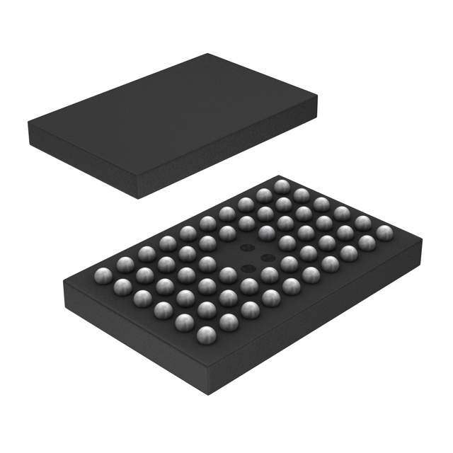
ICGOO电子元器件商城为您提供SN74AVC16244ZQLR由Texas Instruments设计生产,在icgoo商城现货销售,并且可以通过原厂、代理商等渠道进行代购。 SN74AVC16244ZQLR价格参考。Texas InstrumentsSN74AVC16244ZQLR封装/规格:逻辑 - 缓冲器,驱动器,接收器,收发器, Buffer, Non-Inverting 4 Element 4 Bit per Element 3-State Output 56-BGA MICROSTAR JUNIOR (7.0x4.5)。您可以下载SN74AVC16244ZQLR参考资料、Datasheet数据手册功能说明书,资料中有SN74AVC16244ZQLR 详细功能的应用电路图电压和使用方法及教程。
SN74AVC16244ZQLR 是 Texas Instruments 生产的一款逻辑缓冲器、驱动器和接收器,属于 16 位总线收发器系列。它主要用于在不同的电压域之间进行信号转换和传输,特别适用于需要在不同电源电压下工作的系统中。

 应用场景:

1. 电压电平转换:
   - SN74AVC16244ZQLR 支持 1.2V 至 3.6V 的宽输入/输出电压范围,使其非常适合用于低功耗和混合电压系统的电平转换。例如,在一个系统中,某些组件工作在 1.8V,而其他组件工作在 3.3V,这款芯片可以确保这些组件之间的信号能够正确传递而不丢失数据或产生错误。

2. 高速数据传输:
   - 该器件具有较低的传播延迟(通常为几纳秒),适合用于高速数据传输应用,如 DDR 内存接口、FPGA 或 ASIC 与外部设备之间的通信。它可以有效地减少信号失真和延迟,提高系统的整体性能。

3. 多点总线通信:
   - 在多点总线系统中,多个设备共享同一组信号线。SN74AVC16244ZQLR 可以作为总线收发器,控制数据的方向和流量,防止信号冲突并确保每个设备都能可靠地发送和接收数据。这在工业自动化、汽车电子和通信设备中非常常见。

4. 扩展 I/O 端口:
   - 在嵌入式系统设计中,有时需要扩展微控制器或处理器的 I/O 端口。SN74AVC16244ZQLR 可以作为一个双向缓冲器,增加额外的 I/O 线路,同时保持信号的完整性和稳定性。

5. 信号调理和增强:
   - 当信号经过长距离传输或通过噪声环境时,可能会衰减或受到干扰。SN74AVC16244ZQLR 可以增强信号强度,确保信号在到达目的地时仍然保持高质量。这对于远程传感器网络或无线通信模块尤为重要。

总之,SN74AVC16244ZQLR 是一款多功能的逻辑缓冲器和收发器,广泛应用于各种需要高效、可靠信号传输和电压电平转换的场合。其灵活性和高性能使得它成为现代电子系统设计中的重要组件。
| 参数 | 数值 |
| 产品目录 | 集成电路 (IC) |
| 描述 | IC BUFF/DVR TRI-ST 16BIT 56BGA |
| 产品分类 | |
| 品牌 | Texas Instruments |
| 数据手册 | |
| 产品图片 |
|
| 产品型号 | SN74AVC16244ZQLR |
| PCN设计/规格 | |
| rohs | 无铅 / 符合限制有害物质指令(RoHS)规范要求 |
| 产品系列 | 74AVC |
| 产品目录页面 | |
| 供应商器件封装 | 56-BGA MICROSTAR JUNIOR(7.0x4.5) |
| 元件数 | 4 |
| 其它名称 | 296-25439-6 |
| 包装 | Digi-Reel® |
| 安装类型 | 表面贴装 |
| 封装/外壳 | 56-VFBGA |
| 工作温度 | -40°C ~ 85°C |
| 标准包装 | 1 |
| 每元件位数 | 4 |
| 电压-电源 | 1.4 V ~ 3.6 V |
| 电流-输出高,低 | 12mA,12mA |
| 逻辑类型 | 缓冲器/线路驱动器,非反相 |


- 商务部:美国ITC正式对集成电路等产品启动337调查
- 曝三星4nm工艺存在良率问题 高通将骁龙8 Gen1或转产台积电
- 太阳诱电将投资9.5亿元在常州建新厂生产MLCC 预计2023年完工
- 英特尔发布欧洲新工厂建设计划 深化IDM 2.0 战略
- 台积电先进制程称霸业界 有大客户加持明年业绩稳了
- 达到5530亿美元!SIA预计今年全球半导体销售额将创下新高
- 英特尔拟将自动驾驶子公司Mobileye上市 估值或超500亿美元
- 三星加码芯片和SET,合并消费电子和移动部门,撤换高东真等 CEO
- 三星电子宣布重大人事变动 还合并消费电子和移动部门
- 海关总署:前11个月进口集成电路产品价值2.52万亿元 增长14.8%


PDF Datasheet 数据手册内容提取
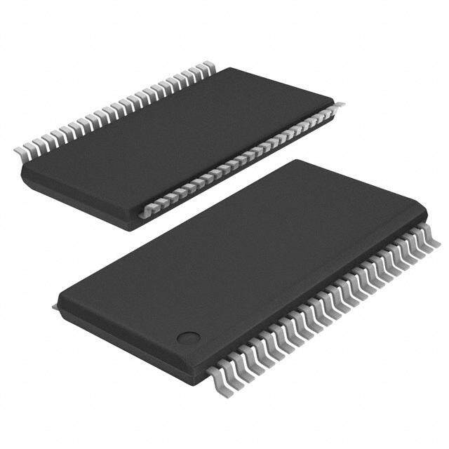
SN74AVC16244 16-BIT BUFFER/DRIVER WITH 3-STATE OUTPUTS www.ti.com SCES141N–JULY1998–REVISEDMARCH2005 FEATURES • Overvoltage-TolerantInputs/OutputsAllow • MemberoftheTexasInstrumentsWidebus™ Mixed-Voltage-ModeDataCommunications Family • I SupportsPartial-Power-DownMode off • DOC™(DynamicOutputControl)Circuit Operation DynamicallyChangesOutputImpedance, • Latch-UpPerformanceExceeds100mAPer ResultinginNoiseReductionWithoutSpeed JESD78,ClassII Degradation • ESDProtectionExceedsJESD22 • LessThan2-nsMaximumPropagationDelay – 2000-VHuman-BodyModel(A114-A) at2.5-Vand3.3-VV CC – 200-VMachineModel(A115-A) • DynamicDriveCapabilityIsEquivalentto StandardOutputsWithI andI of– 24mA OH OL at2.5-VV CC DESCRIPTION/ORDERING INFORMATION A Dynamic Output Control (DOC) circuit is implemented, which, during the transition, initially lowers the output impedancetoeffectivelydrive the load and, subsequently, raises the impedance to reduce noise. Figure 1 shows typical V vs I and V vs I curves to illustrate the output impedance and drive capability of the circuit. At OL OL OH OH the beginning of the signal transition, the DOC circuit provides a maximum dynamic drive that is equivalent to a high-drive standard-output device. For more information, refer to the TI application reports, AVC Logic Family Technology and Applications, literature number SCEA006, and Dynamic Output Control (DOC™) Circuitry TechnologyandApplications,literaturenumberSCEA009. 3.2 TA = 25°C TA = 25°C Process = Nominal 2.8 Process = Nominal 2.8 V V Voltage - 22..04 VCC = 3.3 V Voltage - 22..04 Output 11..26 VCC = 2.5 V Output 11..26 - L VCC = 1.8 V - H VO 0.8 VO 0.8 VCC = 3.3 V VCC = 2.5 V 0.4 0.4 VCC = 1.8 V 0 17 34 51 68 85 102 119 136 153 170 -160 -144 -128 -112 -96 -80 -64 -48 -32 -16 0 IOL - Output Current - mA IOH - Output Current - mA Figure1.OutputVoltagevsOutputCurrent ORDERINGINFORMATION T PACKAGE(1) ORDERABLEPARTNUMBER TOP-SIDEMARKING A TSSOP–DGG Tapeandreel SN74AVC16244DGGR AVC16244 TVSOP–DGV Tapeandreel SN74AVC16244DGVR CVA244 –40(cid:176) Cto85(cid:176) C VFBGA–GQL SN74AVC16244GQLR Tapeandreel CVA244 VFBGA–ZQL(Pb-free) SN74AVC16244ZQLR (1) Packagedrawings,standardpackingquantities,thermaldata,symbolization,andPCBdesignguidelinesareavailableat www.ti.com/sc/package. Pleasebeawarethatanimportantnoticeconcerningavailability,standardwarranty,anduseincriticalapplicationsofTexas Instrumentssemiconductorproductsanddisclaimerstheretoappearsattheendofthisdatasheet. Widebus,DOCaretrademarksofTexasInstruments. PRODUCTIONDATAinformationiscurrentasofpublicationdate. Copyright©1998–2005,TexasInstrumentsIncorporated Products conform to specifications per the terms of the Texas Instruments standard warranty. Production processing does not necessarilyincludetestingofallparameters.
SN74AVC16244 16-BIT BUFFER/DRIVER WITH 3-STATE OUTPUTS www.ti.com SCES141N–JULY1998–REVISEDMARCH2005 DESCRIPTION/ORDERING INFORMATION (CONTINUED) This 16-bit buffer/driver is operational at 1.2-V to 3.6-V V , but is designed specifically for 1.65-V to 3.6-V V CC CC operation. The SN74AVC16244 is designed specifically to improve the performance and density of 3-state memory address drivers,clockdrivers,andbus-orientedreceiversandtransmitters. The device can be used as four 4-bit buffers, two 8-bit buffers, or one 16-bit buffer. It provides true outputs and symmetricalactive-lowoutput-enable(OE)inputs. This device is fully specified for partial-power-down applications using I . The I circuitry disables the outputs, off off preventingdamagingcurrentbackflowthroughthedevicewhenitispowereddown. To ensure the high-impedance state during power up or power down, OE should be tied to V through a pullup CC resistor;theminimumvalueoftheresistorisdeterminedbythecurrent-sinkingcapabilityofthedriver. DGG OR DGV PACKAGE (TOP VIEW) 1OE 1 48 2OE 1Y1 2 47 1A1 1Y2 3 46 1A2 GND 4 45 GND 1Y3 5 44 1A3 1Y4 6 43 1A4 V 7 42 V CC CC 2Y1 8 41 2A1 2Y2 9 40 2A2 GND 10 39 GND 2Y3 11 38 2A3 2Y4 12 37 2A4 3Y1 13 36 3A1 3Y2 14 35 3A2 GND 15 34 GND 3Y3 16 33 3A3 3Y4 17 32 3A4 V 18 31 V CC CC 4Y1 19 30 4A1 4Y2 20 29 4A2 GND 21 28 GND 4Y3 22 27 4A3 4Y4 23 26 4A4 4OE 24 25 3OE 2
SN74AVC16244 16-BIT BUFFER/DRIVER WITH 3-STATE OUTPUTS www.ti.com SCES141N–JULY1998–REVISEDMARCH2005 GQL OR ZQL PACKAGE (TOP VIEW) 1 2 3 4 5 6 A B C D E F G H J K TERMINALASSIGNMENTS(1) 1 2 3 4 5 6 A 1OE NC NC NC NC 2OE B 1Y2 1Y1 GND GND 1A1 1A2 C 1Y4 1Y3 V V 1A3 1A4 CC CC D 2Y2 2Y1 GND GND 2A1 2A2 E 2Y4 2Y3 2A3 2A4 F 3Y1 3Y2 3A2 3A1 G 3Y3 3Y4 GND GND 3A4 3A3 H 4Y1 4Y2 V V 4A2 4A1 CC CC J 4Y3 4Y4 GND GND 4A4 4A3 K 4OE NC NC NC NC 3OE (1) NC-Nointernalconnection FUNCTIONTABLE (EACH4-BITBUFFER) INPUTS OUTPUT OE A Y L L L L H H H X Z 3
SN74AVC16244 16-BIT BUFFER/DRIVER WITH 3-STATE OUTPUTS www.ti.com SCES141N–JULY1998–REVISEDMARCH2005 LOGICDIAGRAM(POSITIVELOGIC) 1 25 1OE 3OE 47 2 36 13 1A1 1Y1 3A1 3Y1 46 3 35 14 1A2 1Y2 3A2 3Y2 44 5 33 16 1A3 1Y3 3A3 3Y3 43 6 32 17 1A4 1Y4 3A4 3Y4 48 24 2OE 4OE 41 8 30 19 2A1 2Y1 4A1 4Y1 40 9 29 20 2A2 2Y2 4A2 4Y2 38 11 27 22 2A3 2Y3 4A3 4Y3 37 12 26 23 2A4 2Y4 4A4 4Y4 Absolute Maximum Ratings(1) overoperatingfree-airtemperaturerange(unlessotherwisenoted) MIN MAX UNIT V Supplyvoltagerange –0.5 4.6 V CC V Inputvoltagerange(2) –0.5 4.6 V I V Voltagerangeappliedtoanyoutputinthehigh-impedanceorpower-offstate(2) –0.5 4.6 V O V Voltagerangeappliedtoanyoutputinthehighorlowstate(2)(3) –0.5 V +0.5 V O CC I Inputclampcurrent V <0 –50 mA IK I I Outputclampcurrent V <0 –50 mA OK O I Continuousoutputcurrent – 50 mA O ContinuouscurrentthrougheachV orGND – 100 mA CC DGGpackage 70 q Packagethermalimpedance(4) DGVpackage 58 (cid:176) C/W JA GQL/ZQLpackage 42 T Storagetemperaturerange –65 150 (cid:176) C stg (1) Stressesbeyondthoselistedunder"absolutemaximumratings"maycausepermanentdamagetothedevice.Thesearestressratings only,andfunctionaloperationofthedeviceattheseoranyotherconditionsbeyondthoseindicatedunder"recommendedoperating conditions"isnotimplied.Exposuretoabsolute-maximum-ratedconditionsforextendedperiodsmayaffectdevicereliability. (2) Theinputandoutputnegative-voltageratingsmaybeexceedediftheinputandoutputcurrentratingsareobserved. (3) Theoutputpositive-voltageratingmaybeexceededupto4.6Vmaximumiftheoutputcurrentratingisobserved. (4) ThepackagethermalimpedanceiscalculatedinaccordancewithJESD51. 4
SN74AVC16244 16-BIT BUFFER/DRIVER WITH 3-STATE OUTPUTS www.ti.com SCES141N–JULY1998–REVISEDMARCH2005 Recommended Operating Conditions(1) MIN MAX UNIT Operating 1.4 3.6 V Supplyvoltage V CC Dataretentiononly 1.2 V =1.2V V CC CC V =1.4Vto1.6V 0.65· V CC CC V High-levelinputvoltage V =1.65Vto1.95V 0.65· V V IH CC CC V =2.3Vto2.7V 1.7 CC V =3Vto3.6V 2 CC V =1.2V GND CC V =1.4Vto1.6V 0.35· V CC CC V Low-levelinputvoltage V =1.65Vto1.95V 0.35· V V IL CC CC V =2.3Vto2.7V 0.7 CC V =3Vto3.6V 0.8 CC V Inputvoltage 0 3.6 V I Activestate 0 V CC V Outputvoltage V O 3-state 0 3.6 V =1.4Vto1.6V –2 CC V =1.65Vto1.95V –4 I Statichigh-leveloutputcurrent(2) CC mA OHS V =2.3Vto2.7V –8 CC V =3Vto3.6V –12 CC V =1.4Vto1.6V 2 CC V =1.65Vto1.95V 4 I Staticlow-leveloutputcurrent(2) CC mA OLS V =2.3Vto2.7V 8 CC V =3Vto3.6V 12 CC D t/D v Inputtransitionriseorfallrate V =1.4Vto3.6V 5 ns/V CC T Operatingfree-airtemperature –40 85 (cid:176) C A (1) AllunusedinputsofthedevicemustbeheldatV orGNDtoensureproperdeviceoperation.RefertotheTIapplicationreport, CC ImplicationsofSloworFloatingCMOSInputs,literaturenumberSCBA004. (2) DynamicdrivecapabilityisequivalenttostandardoutputswithI andI of– 24mAat2.5-VV .SeeFigure1forV vsI andV OH OL CC OL OL OH vsI characteristics.RefertotheTIapplicationreports,AVCLogicFamilyTechnologyandApplications,literaturenumberSCEA006, OH andDynamicOutputControl(DOC™)CircuitryTechnologyandApplications,literaturenumberSCEA009. 5
SN74AVC16244 16-BIT BUFFER/DRIVER WITH 3-STATE OUTPUTS www.ti.com SCES141N–JULY1998–REVISEDMARCH2005 Electrical Characteristics overrecommendedoperatingfree-airtemperaturerange(unlessotherwisenoted) PARAMETER TESTCONDITIONS V MIN TYP(1) MAX UNIT CC I =–100m A 1.4Vto3.6V V –0.2 OHS CC I =–2mA, V =0.91V 1.4V 1.05 OHS IH V I =–4mA, V =1.07V 1.65V 1.2 V OH OHS IH I =–8mA, V =1.7V 2.3V 1.75 OHS IH I =–12mA, V =2V 3V 2.3 OHS IH I =100m A 1.4Vto3.6V 0.2 OLS I =2mA, V =0.49V 1.4V 0.4 OLS IL V I =4mA, V =0.57V 1.65V 0.45 V OL OLS IL I =8mA, V =0.7V 2.3V 0.55 OLS IL I =12mA, V =0.8V 3V 0.7 OLS IL I V =V orGND 3.6V – 2.5 m A I I CC I V orV =3.6V 0 – 10 m A off I O I V =V orGND 3.6V – 10 m A OZ O CC I V =V orGND, I =0 3.6V 40 m A CC I CC O 2.5V 3.5 Controlinputs V =V orGND I CC 3.3V 3.5 C pF i 2.5V 6 Datainputs V =V orGND I CC 3.3V 6 2.5V 6.5 C Outputs V =V orGND pF o O CC 3.3V 6.5 (1) TypicalvaluesaremeasuredatT =25(cid:176) C. A Switching Characteristics overrecommendedoperatingfree-airtemperaturerange(unlessotherwisenoted)(seeFigure2) V =1.5V V =1.8V V =2.5V V =3.3V PARAMETER FROM TO VCC=1.2V C–C0.1V C– C0.15V C–C0.2V C–C0.3V UNIT (INPUT) (OUTPUT) TYP MIN MAX MIN MAX MIN MAX MIN MAX t A Y 3.1 0.6 3.3 0.7 2.9 0.6 1.9 0.5 1.7 ns pd t OE Y 7.6 1.4 8 1.3 6.8 0.9 4 0.7 3.5 ns en t OE Y 7.2 1.7 7.3 1.6 6.2 1 4.3 1 3.5 ns dis Operating Characteristics T =25(cid:176) C A V =1.8V V =2.5V V =3.3V CC CC CC PARAMETER TESTCONDITIONS UNIT TYP TYP TYP Powerdissipation Outputsenabled 23 27 33 C C =0, f=10MHz pF pd capacitance Outputsdisabled L 0.1 0.1 0.1 6
SN74AVC16244 16-BIT BUFFER/DRIVER WITH 3-STATE OUTPUTS www.ti.com SCES141N–JULY1998–REVISEDMARCH2005 PARAMETER MEASUREMENT INFORMATION 2 × VCC TEST S1 From Output RL S1 Open tPLH/tPHL Open Under Test GND tPLZ/tPZL 2 × VCC CL tPHZ/tPZH GND (see Note A) RL VCC CL RL VD 1.2 V 15 pF 2 kW 0.1 V 1.5 V ± 0.1 V 15 pF 2 kW 0.1 V LOAD CIRCUIT 1.8 V ± 0.15 V 30 pF 1 kW 0.15 V 2.5 V ± 0.2 V 30 pF 500 W 0.15 V 3.3 V ± 0.3 V 30 pF 500 W 0.3 V VCC Timing Input VCC/2 0 V tw tsu th VCC VCC Input VCC/2 VCC/2 Data Input VCC/2 VCC/2 0 V 0 V VOLTAGE WAVEFORMS VOLTAGE WAVEFORMS PULSE DURATION SETUP AND HOLD TIMES VCC Output VCC Input VCC/2 VCC/2 Control VCC/2 VCC/2 0 V 0 V tPLH tPHL tPZL tPLZ Output VOH Waveform 1 Output VCC/2 VCC/2 S1 at 2 × VCC VCC/2 VOL + VD VOL (see Note B) VOL tPHL tPLH tPZH tPHZ Output Output VCC/2 VCC/2 VOH WSa1v eafto GrmN D2 VCC/2 VOH - VD VOH VOL (see Note B) ≈0 V VOLTAGE WAVEFORMS VOLTAGE WAVEFORMS PROPAGATION DELAY TIMES ENABLE AND DISABLE TIMES INVERTING AND NONINVERTING OUTPUTS LOW- AND HIGH-LEVEL ENABLING NOTES: A. CL includes probe and jig capacitance. B. Waveform 1 is for an output with internal conditions such that the output is low, except when disabled by the output control. Waveform2 is for an output with internal conditions such that the output is high, except when disabled by the output control. C. All input pulses are supplied by generators having the following characteristics: PRR ≤ 10 MHz, ZO = 50 W , slew rate ≥ 1 V/ns. D. The outputs are measured one at a time, with one transition per measurement. E. tPLZ and tPHZ are the same as tdis. F. tPZL and tPZH are the same as ten. G. tPLH and tPHL are the same as tpd. H. All parameters and waveforms are not applicable to all devices. Figure2.LoadCircuitandVoltageWaveforms 7
PACKAGE OPTION ADDENDUM www.ti.com 24-Aug-2018 PACKAGING INFORMATION Orderable Device Status Package Type Package Pins Package Eco Plan Lead/Ball Finish MSL Peak Temp Op Temp (°C) Device Marking Samples (1) Drawing Qty (2) (6) (3) (4/5) SN74AVC16244DGGR ACTIVE TSSOP DGG 48 2000 Green (RoHS CU NIPDAU Level-1-260C-UNLIM -40 to 85 AVC16244 & no Sb/Br) SN74AVC16244DGVR ACTIVE TVSOP DGV 48 2000 Green (RoHS CU NIPDAU Level-1-260C-UNLIM -40 to 85 CVA244 & no Sb/Br) SN74AVC16244ZQLR ACTIVE BGA ZQL 56 1000 Green (RoHS SNAGCU Level-1-260C-UNLIM -40 to 85 CVA244 MICROSTAR & no Sb/Br) JUNIOR (1) The marketing status values are defined as follows: ACTIVE: Product device recommended for new designs. LIFEBUY: TI has announced that the device will be discontinued, and a lifetime-buy period is in effect. NRND: Not recommended for new designs. Device is in production to support existing customers, but TI does not recommend using this part in a new design. PREVIEW: Device has been announced but is not in production. Samples may or may not be available. OBSOLETE: TI has discontinued the production of the device. (2) RoHS: TI defines "RoHS" to mean semiconductor products that are compliant with the current EU RoHS requirements for all 10 RoHS substances, including the requirement that RoHS substance do not exceed 0.1% by weight in homogeneous materials. Where designed to be soldered at high temperatures, "RoHS" products are suitable for use in specified lead-free processes. TI may reference these types of products as "Pb-Free". RoHS Exempt: TI defines "RoHS Exempt" to mean products that contain lead but are compliant with EU RoHS pursuant to a specific EU RoHS exemption. Green: TI defines "Green" to mean the content of Chlorine (Cl) and Bromine (Br) based flame retardants meet JS709B low halogen requirements of <=1000ppm threshold. Antimony trioxide based flame retardants must also meet the <=1000ppm threshold requirement. (3) MSL, Peak Temp. - The Moisture Sensitivity Level rating according to the JEDEC industry standard classifications, and peak solder temperature. (4) There may be additional marking, which relates to the logo, the lot trace code information, or the environmental category on the device. (5) Multiple Device Markings will be inside parentheses. Only one Device Marking contained in parentheses and separated by a "~" will appear on a device. If a line is indented then it is a continuation of the previous line and the two combined represent the entire Device Marking for that device. (6) Lead/Ball Finish - Orderable Devices may have multiple material finish options. Finish options are separated by a vertical ruled line. Lead/Ball Finish values may wrap to two lines if the finish value exceeds the maximum column width. Important Information and Disclaimer:The information provided on this page represents TI's knowledge and belief as of the date that it is provided. TI bases its knowledge and belief on information provided by third parties, and makes no representation or warranty as to the accuracy of such information. Efforts are underway to better integrate information from third parties. TI has taken and continues to take reasonable steps to provide representative and accurate information but may not have conducted destructive testing or chemical analysis on incoming materials and chemicals. TI and TI suppliers consider certain information to be proprietary, and thus CAS numbers and other limited information may not be available for release. Addendum-Page 1
PACKAGE OPTION ADDENDUM www.ti.com 24-Aug-2018 In no event shall TI's liability arising out of such information exceed the total purchase price of the TI part(s) at issue in this document sold by TI to Customer on an annual basis. Addendum-Page 2
PACKAGE MATERIALS INFORMATION www.ti.com 12-Feb-2019 TAPE AND REEL INFORMATION *Alldimensionsarenominal Device Package Package Pins SPQ Reel Reel A0 B0 K0 P1 W Pin1 Type Drawing Diameter Width (mm) (mm) (mm) (mm) (mm) Quadrant (mm) W1(mm) SN74AVC16244DGGR TSSOP DGG 48 2000 330.0 24.4 8.6 13.0 1.8 12.0 24.0 Q1 SN74AVC16244DGVR TVSOP DGV 48 2000 330.0 16.4 7.1 10.2 1.6 12.0 16.0 Q1 SN74AVC16244ZQLR BGAMI ZQL 56 1000 330.0 16.4 4.8 7.3 1.5 8.0 16.0 Q1 CROSTA RJUNI OR PackMaterials-Page1
PACKAGE MATERIALS INFORMATION www.ti.com 12-Feb-2019 *Alldimensionsarenominal Device PackageType PackageDrawing Pins SPQ Length(mm) Width(mm) Height(mm) SN74AVC16244DGGR TSSOP DGG 48 2000 367.0 367.0 45.0 SN74AVC16244DGVR TVSOP DGV 48 2000 367.0 367.0 38.0 SN74AVC16244ZQLR BGAMICROSTAR ZQL 56 1000 350.0 350.0 43.0 JUNIOR PackMaterials-Page2
MECHANICAL DATA MPDS006C – FEBRUARY 1996 – REVISED AUGUST 2000 DGV (R-PDSO-G**) PLASTIC SMALL-OUTLINE 24 PINS SHOWN 0,23 0,40 0,07 M 0,13 24 13 0,16 NOM 4,50 6,60 4,30 6,20 Gage Plane 0,25 0°–(cid:1)8° 0,75 1 12 0,50 A Seating Plane 0,15 1,20 MAX 0,08 0,05 PINS ** 14 16 20 24 38 48 56 DIM A MAX 3,70 3,70 5,10 5,10 7,90 9,80 11,40 A MIN 3,50 3,50 4,90 4,90 7,70 9,60 11,20 4073251/E 08/00 NOTES: A. All linear dimensions are in millimeters. B. This drawing is subject to change without notice. C. Body dimensions do not include mold flash or protrusion, not to exceed 0,15 per side. D. Falls within JEDEC: 24/48 Pins – MO-153 14/16/20/56 Pins – MO-194 • POST OFFICE BOX 655303 DALLAS, TEXAS 75265
MECHANICAL DATA MTSS003D – JANUARY 1995 – REVISED JANUARY 1998 DGG (R-PDSO-G**) PLASTIC SMALL-OUTLINE PACKAGE 48 PINS SHOWN 0,27 0,50 0,08 M 0,17 48 25 6,20 8,30 6,00 7,90 0,15 NOM Gage Plane 0,25 1 24 0°–8° A 0,75 0,50 Seating Plane 0,15 1,20 MAX 0,10 0,05 PINS ** 48 56 64 DIM A MAX 12,60 14,10 17,10 A MIN 12,40 13,90 16,90 4040078/F 12/97 NOTES: A. All linear dimensions are in millimeters. B. This drawing is subject to change without notice. C. Body dimensions do not include mold protrusion not to exceed 0,15. D. Falls within JEDEC MO-153 • POST OFFICE BOX 655303 DALLAS, TEXAS 75265
PACKAGE OUTLINE ZQL0056A JRBGA - 1 mm max height SCALE 2.100 PLASTIC BALL GRID ARRAY 4.6 B A 4.4 BALL A1 CORNER 7.1 6.9 1 MAX C SEATING PLANE 0.35 0.15 TYP BALL TYP 0.1 C 3.25 TYP SYMM (0.625) TYP K J (0.575) TYP H G 5.85 F SYMM TYP E D C 0.45 56X NOTE 3 0.35 B 0.15 C B A 0.08 C A 0.65 TYP 1 2 3 4 5 6 BALL A1 CORNER 0.65 TYP 4219711/B 01/2017 NOTES: 1. All linear dimensions are in millimeters. Any dimensions in parenthesis are for reference only. Dimensioning and tolerancing per ASME Y14.5M. 2. This drawing is subject to change without notice. 3. No metal in this area, indicates orientation. www.ti.com
EXAMPLE BOARD LAYOUT ZQL0056A JRBGA - 1 mm max height PLASTIC BALL GRID ARRAY (0.65) TYP 56X ( 0.33) 1 2 3 4 5 6 A (0.65) TYP B C D E SYMM F G H J K SYMM LAND PATTERN EXAMPLE EXPOSED METAL SHOWN SCALE:15X SOLDER MASK 0.05 MAX 0.05 MIN METAL UNDER OPENING SOLDER MASK EXPOSED METAL ( 0.33) ( 0.33) METAL EXPOSED METAL SOLDER MASK OPENING NON-SOLDER MASK SOLDER MASK DEFINED DEFINED (PREFERRED) SOLDER MASK DETAILS NOT TO SCALE 4219711/B 01/2017 NOTES: (continued) 4. Final dimensions may vary due to manufacturing tolerance considerations and also routing constraints. For information, see Texas Instruments literature number SPRAA99 (www.ti.com/lit/spraa99). www.ti.com
EXAMPLE STENCIL DESIGN ZQL0056A JRBGA - 1 mm max height PLASTIC BALL GRID ARRAY 56X ( 0.33) (0.65) TYP 1 2 3 4 5 6 A (0.65) TYP B C D E SYMM F G H J K SYMM SOLDER PASTE EXAMPLE BASED ON 0.125 mm THICK STENCIL SCALE:15X 4219711/B 01/2017 NOTES: (continued) 5. Laser cutting apertures with trapezoidal walls and rounded corners may offer better paste release. www.ti.com
IMPORTANTNOTICEANDDISCLAIMER TIPROVIDESTECHNICALANDRELIABILITYDATA(INCLUDINGDATASHEETS),DESIGNRESOURCES(INCLUDINGREFERENCE DESIGNS),APPLICATIONOROTHERDESIGNADVICE,WEBTOOLS,SAFETYINFORMATION,ANDOTHERRESOURCES“ASIS” ANDWITHALLFAULTS,ANDDISCLAIMSALLWARRANTIES,EXPRESSANDIMPLIED,INCLUDINGWITHOUTLIMITATIONANY IMPLIEDWARRANTIESOFMERCHANTABILITY,FITNESSFORAPARTICULARPURPOSEORNON-INFRINGEMENTOFTHIRD PARTYINTELLECTUALPROPERTYRIGHTS. TheseresourcesareintendedforskilleddevelopersdesigningwithTIproducts.Youaresolelyresponsiblefor(1)selectingtheappropriate TIproductsforyourapplication,(2)designing,validatingandtestingyourapplication,and(3)ensuringyourapplicationmeetsapplicable standards,andanyothersafety,security,orotherrequirements.Theseresourcesaresubjecttochangewithoutnotice.TIgrantsyou permissiontousetheseresourcesonlyfordevelopmentofanapplicationthatusestheTIproductsdescribedintheresource.Other reproductionanddisplayoftheseresourcesisprohibited.NolicenseisgrantedtoanyotherTIintellectualpropertyrightortoanythird partyintellectualpropertyright.TIdisclaimsresponsibilityfor,andyouwillfullyindemnifyTIanditsrepresentativesagainst,anyclaims, damages,costs,losses,andliabilitiesarisingoutofyouruseoftheseresources. TI’sproductsareprovidedsubjecttoTI’sTermsofSale(www.ti.com/legal/termsofsale.html)orotherapplicabletermsavailableeitheron ti.comorprovidedinconjunctionwithsuchTIproducts.TI’sprovisionoftheseresourcesdoesnotexpandorotherwisealterTI’sapplicable warrantiesorwarrantydisclaimersforTIproducts. MailingAddress:TexasInstruments,PostOfficeBox655303,Dallas,Texas75265 Copyright©2019,TexasInstrumentsIncorporated