ICGOO在线商城 > 集成电路(IC) > 逻辑 - 缓冲器,驱动器,接收器,收发器 > 74HCT2G34GV,125
 Datasheet下载
- 型号: 74HCT2G34GV,125
- 制造商: NXP Semiconductors
- 库位|库存: xxxx|xxxx
- 要求:
| 数量阶梯 | 香港交货 | 国内含税 |
| +xxxx | $xxxx | ¥xxxx |
查看当月历史价格
查看今年历史价格
74HCT2G34GV,125产品简介:
ICGOO电子元器件商城为您提供74HCT2G34GV,125由NXP Semiconductors设计生产,在icgoo商城现货销售,并且可以通过原厂、代理商等渠道进行代购。 74HCT2G34GV,125价格参考¥1.29-¥4.26。NXP Semiconductors74HCT2G34GV,125封装/规格:逻辑 - 缓冲器,驱动器,接收器,收发器, Buffer, Non-Inverting 2 Element 1 Bit per Element Push-Pull Output 6-TSOP。您可以下载74HCT2G34GV,125参考资料、Datasheet数据手册功能说明书,资料中有74HCT2G34GV,125 详细功能的应用电路图电压和使用方法及教程。
Nexperia USA Inc.生产的74HCT2G34GV,125是一款逻辑缓冲器,属于74HCT系列的双路非门(Inverter)芯片。它主要应用于需要信号反转、电平转换和驱动能力增强的场景。以下是其主要应用场景:

 1. 数字信号处理
   - 该芯片常用于数字电路中,对输入信号进行反转处理。例如,在时钟信号生成或数据传输过程中,需要将信号反转以满足特定逻辑需求。
   - 可用于触发器、计数器或其他逻辑电路的输入/输出信号处理。

 2. 电平转换
   - 74HCT2G34GV支持TTL到CMOS电平转换。由于其输入兼容TTL电平,而输出为CMOS电平,因此可以用来连接不同电平标准的设备。
   - 适用于微控制器与外围设备之间的信号接口设计。

 3. 驱动能力增强
   - 当输入信号源无法提供足够的电流驱动负载时,该芯片可以用作信号驱动器,增强信号的驱动能力。
   - 例如,驱动LED指示灯、小型继电器或其他低功耗器件。

 4. 通信接口
   - 在串行通信或并行通信中,作为信号缓冲或反转使用。例如,在UART、SPI或I2C等通信协议中,可能需要信号反转或增强来确保信号完整性。

 5. 音频和视频信号处理
   - 在一些简单的音频或视频信号处理电路中,该芯片可用于信号反转或同步信号生成。

 6. 工业控制
   - 工业自动化系统中,常需要对传感器信号进行处理或反转。该芯片可作为信号调理的一部分,用于优化信号传输。

 特性总结:
- 工作电压:2V至6V,适合多种电源环境。
- 高输入阻抗:减少信号源负载。
- 快速开关速度:适合高频应用。
- 低功耗:适用于便携式或电池供电设备。

总之,74HCT2G34GV,125是一款通用性强、性能稳定的逻辑缓冲器,广泛应用于消费电子、工业控制、通信设备等领域,尤其适合需要信号反转和电平转换的场合。
| 参数 | 数值 |
| 产品目录 | 集成电路 (IC)半导体 |
| 描述 | IC BUFFER DL NON-INV 6TSOP缓冲器和线路驱动器 5V DUAL BUFFER GATE |
| 产品分类 | |
| 品牌 | NXP Semiconductors |
| 产品手册 | |
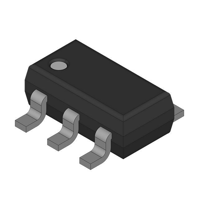
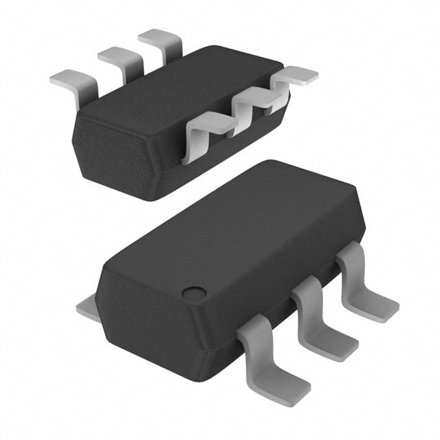
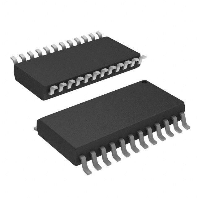
| 产品图片 |
|
| rohs | 符合RoHS无铅 / 符合限制有害物质指令(RoHS)规范要求 |
| 产品系列 | 逻辑集成电路,缓冲器和线路驱动器,NXP Semiconductors 74HCT2G34GV,12574HCT |
| 数据手册 | |
| 产品型号 | 74HCT2G34GV,125 |
| 产品培训模块 | http://www.digikey.cn/PTM/IndividualPTM.page?site=cn&lang=zhs&ptm=24983 |
| 产品种类 | 缓冲器和线路驱动器 |
| 传播延迟时间 | 18 ns at 4.5 V |
| 低电平输出电流 | 4 mA |
| 供应商器件封装 | 6-TSOP |
| 元件数 | 2 |
| 其它名称 | 74HCT2G34GV-G |
| 包装 | 带卷 (TR) |
| 商标 | NXP Semiconductors |
| 安装类型 | 表面贴装 |
| 安装风格 | SMD/SMT |
| 封装 | Reel |
| 封装/外壳 | SC-74,SOT-457 |
| 封装/箱体 | TSOP-6 |
| 工作温度 | -40°C ~ 125°C |
| 工厂包装数量 | 3000 |
| 最大工作温度 | + 125 C |
| 最小工作温度 | - 40 C |
| 极性 | Non-Inverting |
| 标准包装 | 3,000 |
| 每元件位数 | 1 |
| 每芯片的通道数量 | 2 |
| 电压-电源 | 4.5 V ~ 5.5 V |
| 电流-输出高,低 | 4mA,4mA |
| 电源电压-最大 | 5.5 V |
| 电源电压-最小 | 4.5 V |
| 输入线路数量 | 2 |
| 输出线路数量 | 2 |
| 逻辑类型 | CMOS |
| 逻辑系列 | HCT |
| 零件号别名 | 74HCT2G34GV-G |
| 高电平输出电流 | - 4 mA |


- 商务部:美国ITC正式对集成电路等产品启动337调查
- 曝三星4nm工艺存在良率问题 高通将骁龙8 Gen1或转产台积电
- 太阳诱电将投资9.5亿元在常州建新厂生产MLCC 预计2023年完工
- 英特尔发布欧洲新工厂建设计划 深化IDM 2.0 战略
- 台积电先进制程称霸业界 有大客户加持明年业绩稳了
- 达到5530亿美元!SIA预计今年全球半导体销售额将创下新高
- 英特尔拟将自动驾驶子公司Mobileye上市 估值或超500亿美元
- 三星加码芯片和SET,合并消费电子和移动部门,撤换高东真等 CEO
- 三星电子宣布重大人事变动 还合并消费电子和移动部门
- 海关总署:前11个月进口集成电路产品价值2.52万亿元 增长14.8%


PDF Datasheet 数据手册内容提取
74HC2G34; 74HCT2G34 Dual buffer gate Rev. 01 — 6 October 2006 Product data sheet 1. General description The 74HC2G34; 74HCT2G34 is a high-speed Si-gate CMOS device. The 74HC2G34; 74HCT2G34 provides two buffers. 2. Features n Wide supply voltage range from 2.0 Vto6.0V n Complies with JEDEC standard no. 7A n High noise immunity n ESD protection: u HBM JESD22-A114-D exceeds 2000V u MM JESD22-A115-A exceeds 200V n Low power dissipation n Balanced propagation delays n Unlimited input rise and fall times n Multiple package options n Specified from-40 (cid:176)Cto+85(cid:176)C and -40 (cid:176)Cto+125 (cid:176)C 3. Ordering information Table 1. Ordering information Type number Package Temperature range Name Description Version 74HC2G34GW -40 (cid:176)C to +125 (cid:176)C SC-88 plastic surface-mounted package; 6 leads SOT363 74HC2G34GV -40 (cid:176)C to +125 (cid:176)C SC-74 plastic surface-mounted package (TSOP6); 6 leads SOT457 74HCT2G34GW -40 (cid:176)C to +125 (cid:176)C SC-88 plastic surface-mounted package; 6 leads SOT363 74HCT2G34GV -40 (cid:176)C to +125 (cid:176)C SC-74 plastic surface-mounted package (TSOP6); 6 leads SOT457 4. Marking Table 2. Marking Type number Marking code 74HC2G34GW PA 74HC2G34GV P34 74HCT2G34GW UA 74HCT2G34GV U34
74HC2G34; 74HCT2G34 Nexperia Dual buffer gate 5. Functional diagram 1 1A 1Y 6 1 1 6 3 2A 2Y 4 1 3 4 A Y mnb063 mnb064 001aac536 Fig 1. Logic symbol Fig 2. IEC logic symbol Fig 3. Logic diagram (one gate) 6. Pinning information 6.1 Pinning 74HC2G34 74HCT2G34 1A 1 6 1Y GND 2 5 VCC 2A 3 4 2Y 001aaf303 Fig 4. Pin configuration 6.2 Pin description Table 3. Pin description Symbol Pin Description 1A 1 data input GND 2 ground (0V) 2A 3 data input 2Y 4 data output V 5 supply voltage CC 1Y 6 data output 74HC_HCT2G34_1 © Nexperia B.V. 2017. All rights reserved Product data sheet Rev. 01 — 6 October 2006 2 of 14
74HC2G34; 74HCT2G34 Nexperia Dual buffer gate 7. Functional description Table 4. Function table[1] Input Output nA nY L L H H [1] H=HIGH voltage level; L=LOW voltage level. 8. Limiting values Table 5. Limiting values In accordance with the Absolute Maximum Rating System (IEC 60134). Voltages are referenced to GND (ground = 0 V). Symbol Parameter Conditions Min Max Unit V supply voltage -0.5 +7.0 V CC I input clamping current V <-0.5V or V >V +0.5 V [1] - –20 mA IK I I CC I output clamping current V <-0.5V or V >V +0.5V [1] - –20 mA OK O O CC I output current V =-0.5V to V +0.5V [1] - –25 mA O O CC I supply current [1] - +50 mA CC I ground current [1] - -50 mA GND T storage temperature -65 +150 (cid:176)C stg P total power dissipation [2] - 250 mW tot [1] The minimum input and output voltage ratings may be exceeded if the input and output current ratings are observed. [2] For SC-88 and SC-74 packages: above 87.5(cid:176)C the value of P derates linearly with 4.0mW/K. tot 9. Recommended operating conditions Table 6. Recommended operating conditions Symbol Parameter Conditions Min Typ Max Unit Type 74HC2G34 V supply voltage 2.0 5.0 6.0 V CC V input voltage 0 - V V I CC V output voltage 0 - V V O CC T ambient temperature -40 +25 +125 (cid:176)C amb t rise time except for Schmitt trigger inputs r V = 2.0V - - 1000 ns CC V = 4.5V - - 500 ns CC V = 6.0V - - 400 ns CC t fall time except for Schmitt trigger inputs f V = 2.0V - - 1000 ns CC V = 4.5V - - 500 ns CC V = 6.0V - - 400 ns CC 74HC_HCT2G34_1 © Nexperia B.V. 2017. All rights reserved Product data sheet Rev. 01 — 6 October 2006 3 of 14
74HC2G34; 74HCT2G34 Nexperia Dual buffer gate Table 6. Recommended operating conditions …continued Symbol Parameter Conditions Min Typ Max Unit Type 74HCT2G34 V supply voltage 4.5 5.0 5.5 V CC V input voltage 0 - V V I CC V output voltage 0 - V V O CC T ambient temperature -40 +25 +125 (cid:176)C amb t rise time except for Schmitt trigger inputs r V = 4.5V - - 500 ns CC t fall time except for Schmitt trigger inputs f V = 4.5V - - 500 ns CC 10. Static characteristics Table 7. Static characteristics for 74HC2G34 At recommended operating conditions; voltages are referenced to GND (ground=0V). Symbol Parameter Conditions Min Typ Max Unit T = 25(cid:176)C amb V HIGH-level input voltage V = 2.0V 1.5 1.2 - V IH CC V = 4.5V 3.15 2.4 - V CC V = 6.0V 4.2 3.2 - V CC V LOW-level input voltage V = 2.0V - 0.8 0.5 V IL CC V = 4.5V - 2.1 1.35 V CC V = 6.0V - 2.8 1.8 V CC V HIGH-level output voltage V = V or V OH I IH IL I =-20 m A; V = 2.0V 1.9 2.0 - V O CC I =-20 m A; V = 4.5V 4.4 4.5 - V O CC I =-20 m A; V = 6.0V 5.9 6.0 - V O CC I =-4.0mA; V =4.5V 4.18 4.32 - V O CC I =-5.2mA; V =6.0V 5.68 5.81 - V O CC V LOW-level output voltage V = V or V OL I IH IL I = 20mA; V = 2.0V - 0 0.1 V O CC I = 20mA; V = 4.5V - 0 0.1 V O CC I = 20mA; V = 6.0V - 0 0.1 V O CC I = 4.0mA; V = 4.5V - 0.15 0.26 V O CC I = 5.2mA; V = 6.0V - 0.16 0.26 V O CC I input leakage current V = GND or V ; V = 6.0V - - –0.1 mA I I CC CC I supply current V = GND or V ; I = 0 A; - - 1.0 mA CC I CC O V = 6.0V CC C input capacitance - 1.5 - pF I 74HC_HCT2G34_1 © Nexperia B.V. 2017. All rights reserved Product data sheet Rev. 01 — 6 October 2006 4 of 14
74HC2G34; 74HCT2G34 Nexperia Dual buffer gate Table 7. Static characteristics for 74HC2G34 …continued At recommended operating conditions; voltages are referenced to GND (ground=0V). Symbol Parameter Conditions Min Typ Max Unit T =-40 (cid:176)C to +85 (cid:176)C amb V HIGH-level input voltage V = 2.0V 1.5 - - V IH CC V = 4.5V 3.15 - - V CC V = 6.0V 4.2 - - V CC V LOW-level input voltage V = 2.0V - - 0.5 V IL CC V = 4.5V - - 1.35 V CC V = 6.0V - - 1.8 V CC V HIGH-level output voltage V = V or V OH I IH IL I =-20 m A; V = 2.0V 1.9 - - V O CC I =-20 m A; V = 4.5V 4.4 - - V O CC I =-20 m A; V = 6.0V 5.9 - - V O CC I =-4.0mA; V = 4.5V 4.13 - - V O CC I =-5.2mA; V = 6.0V 5.63 - - V O CC V LOW-level output voltage V = V or V OL I IH IL I = 20mA; V = 2.0V - - 0.1 V O CC I = 20mA; V = 4.5V - - 0.1 V O CC I = 20mA; V = 6.0V - - 0.1 V O CC I = 4.0mA; V = 4.5V - - 0.33 V O CC I = 5.2mA; V = 6.0V - - 0.33 V O CC I input leakage current V = GND or V ; V = 6.0V - - –1.0 mA I I CC CC I supply current V = GND or V ; I = 0 A; - - 10.0 mA CC I CC O V = 6.0V CC T =-40 (cid:176)C to +125 (cid:176)C amb V HIGH-level input voltage V = 2.0V 1.5 - - V IH CC V = 4.5V 3.15 - - V CC V = 6.0V 4.2 - - V CC V LOW-level input voltage V = 2.0V - - 0.5 V IL CC V = 4.5V - - 1.35 V CC V = 6.0V - - 1.8 V CC V HIGH-level output voltage V = V or V OH I IH IL I =-20 m A; V = 2.0V 1.9 - - V O CC I =-20 m A; V = 4.5V 4.4 - - V O CC I =-20 m A; V = 6.0V 5.9 - - V O CC I =-4.0mA; V = 4.5V 3.7 - - V O CC I =-5.2mA; V = 6.0V 5.2 - - V O CC 74HC_HCT2G34_1 © Nexperia B.V. 2017. All rights reserved Product data sheet Rev. 01 — 6 October 2006 5 of 14
74HC2G34; 74HCT2G34 Nexperia Dual buffer gate Table 7. Static characteristics for 74HC2G34 …continued At recommended operating conditions; voltages are referenced to GND (ground=0V). Symbol Parameter Conditions Min Typ Max Unit V LOW-level output voltage V = V or V OL I IH IL I = 20mA; V = 2.0V - - 0.1 V O CC I = 20mA; V = 4.5V - - 0.1 V O CC I = 20mA; V = 6.0V - - 0.1 V O CC I = 4.0mA; V = 4.5V - - 0.4 V O CC I = 5.2mA; V = 6.0V - - 0.4 V O CC I input leakage current V = GND or V ; V = 6.0V - - –1.0 mA I I CC CC I supply current V = GND or V ; I = 0 A; - - 20.0 mA CC I CC O V = 6.0V CC Table 8. Static characteristics for 74HCT2G34 At recommended operating conditions; voltages are referenced to GND (ground=0V). Symbol Parameter Conditions Min Typ Max Unit T = 25(cid:176)C amb V HIGH-level input voltage V = 4.5V to 5.5V 2.0 1.6 - V IH CC V LOW-level input voltage V = 4.5V to 5.5V - 1.2 0.8 V IL CC V HIGH-level output voltage V = V or V OH I IH IL I =-20 m A; V = 4.5V 4.4 4.5 - V O CC I =-4.0mA; V = 4.5V 4.18 4.32 - V O CC V LOW-level output voltage V = V or V OL I IH IL I = 20m A; V = 4.5V - 0 0.1 V O CC I = 4.0mA; V = 4.5V - 0.15 0.26 V O CC I input leakage current V = GND or V ; V = 5.5V - - – 0.1 mA I I CC CC I supply current V = GND or V ; I = 0A; - - 1.0 mA CC I CC O V = 5.5V CC DI additional supply current V = V - 2.1V; - - 300 mA CC I CC V =4.5Vto 5.5V; I = 0 A CC O C input capacitance - 1.5 - pF I T =-40 (cid:176)C to +85 (cid:176)C amb V HIGH-level input voltage V = 4.5V to 5.5V 2.0 - - V IH CC V LOW-level input voltage V = 4.5V to 5.5V - - 0.8 V IL CC V HIGH-level output voltage V = V or V OH I IH IL I =-20 m A; V = 4.5V 4.4 - - V O CC I =-4.0mA; V = 4.5V 4.13 - - V O CC V LOW-level output voltage V = V or V OL I IH IL I = 20m A; V = 4.5V - - 0.1 V O CC I = 4.0mA; V = 4.5V - - 0.33 V O CC I input leakage current V = GND or V ; V = 5.5V - - – 1.0 mA I I CC CC I supply current V = GND or V ; I = 0A; - - 10.0 mA CC I CC O V = 5.5V CC DI additional supply current V = V - 2.1V; - - 375 mA CC I CC V =4.5Vto 5.5V; I = 0 A CC O 74HC_HCT2G34_1 © Nexperia B.V. 2017. All rights reserved Product data sheet Rev. 01 — 6 October 2006 6 of 14
74HC2G34; 74HCT2G34 Nexperia Dual buffer gate Table 8. Static characteristics for 74HCT2G34 …continued At recommended operating conditions; voltages are referenced to GND (ground=0V). Symbol Parameter Conditions Min Typ Max Unit T =-40 (cid:176)C to +125 (cid:176)C amb V HIGH-level input voltage V = 4.5V to 5.5V 2.0 - - V IH CC V LOW-level input voltage V = 4.5V to 5.5V - - 0.8 V IL CC V HIGH-level output voltage V = V or V OH I IH IL I =-20 m A; V = 4.5V 4.4 - - V O CC I =-4.0mA; V = 4.5V 3.7 - - V O CC V LOW-level output voltage V = V or V OL I IH IL I = 20m A; V = 4.5V - - 0.1 V O CC I = 4.0mA; V = 4.5V - - 0.4 V O CC I input leakage current V = GND or V ; V = 5.5V - - – 1.0 mA I I CC CC I supply current V = GND or V ; I = 0A; - - 20.0 mA CC I CC O V = 5.5V CC DI additional supply current V = V - 2.1V; - - 410 mA CC I CC V =4.5Vto 5.5V; I = 0 A CC O 11. Dynamic characteristics Table 9. Dynamic characteristics Voltages are referenced to GND (ground=0V); for test circuit seeFigure6. Symbol Parameter Conditions 25(cid:176)C -40 (cid:176)C to+125 (cid:176)C Unit Min Typ Max Min Max Max (85(cid:176)C) (125(cid:176)C) 74HC2G34 t propagation delay nA to nY; seeFigure5 [1] pd V =2.0 V; C =50pF - 29 75 - 95 125 ns CC L V =4.5 V; C =50pF - 9 15 - 19 25 ns CC L V =6.0V; C =50pF - 8 13 - 16 20 ns CC L t transition time nY; seeFigure5 [2] t V = 2.0V; C =50pF - 18 75 - 95 125 ns CC L V = 4.5V; C =50pF - 6 15 - 19 25 ns CC L V = 6.0V; C =50pF - 5 13 - 16 20 ns CC L C power dissipation V = GND to V [3] - 10 - - - - pF PD I CC capacitance 74HC_HCT2G34_1 © Nexperia B.V. 2017. All rights reserved Product data sheet Rev. 01 — 6 October 2006 7 of 14
74HC2G34; 74HCT2G34 Nexperia Dual buffer gate Table 9. Dynamic characteristics …continued Voltages are referenced to GND (ground=0V); for test circuit seeFigure6. Symbol Parameter Conditions 25(cid:176)C -40 (cid:176)C to+125 (cid:176)C Unit Min Typ Max Min Max Max (85(cid:176)C) (125(cid:176)C) 74HCT2G34 t propagation delay nA to nY; seeFigure5 [1] pd V = 4.5V; C =50pF - 10 18 - 23 29 ns CC L t transition time nY; seeFigure5 [2] t V =4.5V; C =50 pF - 6 15 - 19 25 ns CC L C power dissipation V = GND to V - 1.5 V [3] - 9 - - - - pF PD I CC capacitance [1] t is the same as t and t pd PLH PHL [2] t is the same as t and t t TLH THL [3] C is used to determine the dynamic power dissipation (P inm W). PD D P =C · V 2· f · N+S(C · V 2· f ) where: D PD CC i L CC o f =input frequency in MHz; i f =output frequency in MHz; o C =output load capacitance in pF; L V =supply voltage in V; CC N=number of inputs switching; S (C · V 2· f )=sum of the outputs. L CC o 12. Waveforms VI nA input VM VM GND tPLH tPHL VOH 90 % 90 % nY output 10 % 10 % VOL tTLH tTHL 001aaf302 Measurement points are given inTable10. V and V are typical voltage output drop that occur with the output load. OL OH Fig 5. The data input (nA) to output (nY) propagation delays and output transition times Table 10. Measurement points Type Input Output V V t = t V M I r f M 74HC2G34 0.5V GND to V 6.0 ns 0.5V CC CC CC 74HCT2G34 1.3V GND to 3.0 V 6.0 ns 1.3V 74HC_HCT2G34_1 © Nexperia B.V. 2017. All rights reserved Product data sheet Rev. 01 — 6 October 2006 8 of 14
74HC2G34; 74HCT2G34 Nexperia Dual buffer gate V V CC CC PULSE VI VO RL = 1 kW D.U.T open GENERATOR RT CL 50 pF mgk563 Test data is given inTable11. Definitions test circuit: R = Load resistance. L C = Load capacitance including jig and probe capacitance. L R = Termination resistance should be equal to output impedance Z of the pulse generator. T o Fig 6. Load circuitry for switching times Table 11. Test data Type Input Test V t, t t , t I r f PHL PLH 74HC2G34 GND to V 6ns open CC 74HCT2G34 GND to 3.0 V 6ns open 74HC_HCT2G34_1 © Nexperia B.V. 2017. All rights reserved Product data sheet Rev. 01 — 6 October 2006 9 of 14
74HC2G34; 74HCT2G34 Nexperia Dual buffer gate 13. Package outline Plastic surface-mounted package; 6 leads SOT363 D B E A X y HE v M A 6 5 4 Q pin 1 index A A1 1 2 3 c e1 bp w M B Lp e detail X 0 1 2 mm scale DIMENSIONS (mm are the original dimensions) A1 UNIT A max bp c D E e e1 HE Lp Q v w y 1.1 0.30 0.25 2.2 1.35 2.2 0.45 0.25 mm 0.1 1.3 0.65 0.2 0.2 0.1 0.8 0.20 0.10 1.8 1.15 2.0 0.15 0.15 OUTLINE REFERENCES EUROPEAN ISSUE DATE VERSION IEC JEDEC JEITA PROJECTION 04-11-08 SOT363 SC-88 06-03-16 Fig 7. Package outline SOT363 (SC-88) 74HC_HCT2G34_1 © Nexperia B.V. 2017. All rights reserved Product data sheet Rev. 01 — 6 October 2006 10 of 14
74HC2G34; 74HCT2G34 Nexperia Dual buffer gate Plastic surface-mounted package (TSOP6); 6 leads SOT457 D B E A X y HE v M A 6 5 4 Q pin 1 index A A1 c 1 2 3 Lp e bp w M B detail X 0 1 2 mm scale DIMENSIONS (mm are the original dimensions) UNIT A A1 bp c D E e HE Lp Q v w y 1.1 0.1 0.40 0.26 3.1 1.7 3.0 0.6 0.33 mm 0.95 0.2 0.2 0.1 0.9 0.013 0.25 0.10 2.7 1.3 2.5 0.2 0.23 OUTLINE REFERENCES EUROPEAN ISSUE DATE VERSION IEC JEDEC JEITA PROJECTION 05-11-07 SOT457 SC-74 06-03-16 Fig 8. Package outline SOT457 (SC-74) 74HC_HCT2G34_1 © Nexperia B.V. 2017. All rights reserved Product data sheet Rev. 01 — 6 October 2006 11 of 14
74HC2G34; 74HCT2G34 Nexperia Dual buffer gate 14. Abbreviations Table 12. Abbreviations Acronym Description CMOS Complementary Metal Oxide Semiconductor ESD ElectroStatic Discharge HBM Human Body Model MM Machine Model DUT Device Under Test 15. Revision history Table 13. Revision history Document ID Release date Data sheet status Change notice Supersedes 74HC_HCT2G34_1 20061006 Product data sheet - - 74HC_HCT2G34_1 © Nexperia B.V. 2017. All rights reserved Product data sheet Rev. 01 — 6 October 2006 12 of 14
74HC2G34; 74HCT2G34 Nexperia Dual buffer gate 16. Legal information 16.1 Data sheet status Document status[1][2] Product status[3] Definition Objective [short] data sheet Development This document contains data from the objective specification for product development. Preliminary [short] data sheet Qualification This document contains data from the preliminary specification. Product [short] data sheet Production This document contains the product specification. [1] Please consult the most recently issued document before initiating or completing a design. [2] The term ‘short data sheet’ is explained in section “Definitions”. [3] Theproductstatusofdevice(s)describedinthisdocumentmayhavechangedsincethisdocumentwaspublishedandmaydifferincaseofmultipledevices.Thelatestproductstatus information is available on the Internet at URLhttp://www.nexperia.com. 16.2 Definitions malfunctionofaNexperiaproductcanreasonablybeexpectedto result in personal injury, death or severe property or environmental damage. Nexperia accepts no liability for inclusion and/or use of Nexperia Draft —The document is a draft version only. The content is still under products in such equipment or applications and therefore internal review and subject to formal approval, which may result in such inclusion and/or use is at the customer’s own risk. modifications or additions. Nexperia does not give any representations or warranties as to the accuracy or completeness of Applications —Applications that are described herein for any of these informationincludedhereinandshallhavenoliabilityfortheconsequencesof products are for illustrative purposes only. Nexperia makes no use of such information. representation or warranty that such applications will be suitable for the specified use without further testing or modification. Short data sheet —A short data sheet is an extract from a full data sheet withthesameproducttypenumber(s)andtitle.Ashortdatasheetisintended Limiting values —Stress above one or more limiting values (as defined in forquickreferenceonlyandshouldnotbereliedupontocontaindetailedand theAbsoluteMaximumRatingsSystemofIEC60134)maycausepermanent full information. For detailed and full information see the relevant full data damagetothedevice.Limitingvaluesarestressratingsonlyandoperationof sheet, which is available on request via the local Nexperia sales the device at these or any other conditions above those given in the office. In case of any inconsistency or conflict with the short data sheet, the Characteristics sections of this document is not implied. Exposure to limiting full data sheet shall prevail. values for extended periods may affect device reliability. Terms and conditions of sale —Nexperia products are sold 16.3 Disclaimers subjecttothegeneraltermsandconditionsofcommercialsale,aspublished athttp://www.nexperia.com/profile/terms, including those pertaining to warranty, intellectual property rights infringement and limitation of liability, unless General —Information in this document is believed to be accurate and explicitly otherwise agreed to in writing by Nexperia. In case of reliable.However,Nexperiadoesnotgiveanyrepresentationsor any inconsistency or conflict between information in this document and such warranties,expressedorimplied,astotheaccuracyorcompletenessofsuch terms and conditions, the latter will prevail. information and shall have no liability for the consequences of use of such No offer to sell or license —Nothing in this document may be interpreted information. or construed as an offer to sell products that is open for acceptance or the Right to make changes —Nexperiareservestherighttomake grant,conveyanceorimplicationofanylicenseunderanycopyrights,patents changes to information published in this document, including without or other industrial or intellectual property rights. limitation specifications and product descriptions, at any time and without notice.Thisdocumentsupersedesandreplacesallinformationsuppliedprior to the publication hereof. 16.4 Trademarks Suitability for use —Nexperia products are not designed, Notice:Allreferencedbrands,productnames,servicenamesandtrademarks authorized or warranted to be suitable for use in medical, military, aircraft, are the property of their respective owners. space or life support equipment, nor in applications where failure or 17. Contact information For additional information, please visit:http://www.nexperia.com For sales office addresses, send an email to:salesaddresses@nexperia.com 74HC_HCT2G34_1 © Nexperia B.V. 2017. All rights reserved Product data sheet Rev. 01 — 6 October 2006 13 of 14
74HC2G34; 74HCT2G34 Nexperia Dual buffer gate 18. Contents 1 General description. . . . . . . . . . . . . . . . . . . . . . 1 2 Features . . . . . . . . . . . . . . . . . . . . . . . . . . . . . . . 1 3 Ordering information. . . . . . . . . . . . . . . . . . . . . 1 4 Marking. . . . . . . . . . . . . . . . . . . . . . . . . . . . . . . . 1 5 Functional diagram . . . . . . . . . . . . . . . . . . . . . . 2 6 Pinning information. . . . . . . . . . . . . . . . . . . . . . 2 6.1 Pinning . . . . . . . . . . . . . . . . . . . . . . . . . . . . . . . 2 6.2 Pin description . . . . . . . . . . . . . . . . . . . . . . . . . 2 7 Functional description . . . . . . . . . . . . . . . . . . . 3 8 Limiting values. . . . . . . . . . . . . . . . . . . . . . . . . . 3 9 Recommended operating conditions. . . . . . . . 3 10 Static characteristics. . . . . . . . . . . . . . . . . . . . . 4 11 Dynamic characteristics . . . . . . . . . . . . . . . . . . 7 12 Waveforms . . . . . . . . . . . . . . . . . . . . . . . . . . . . . 8 13 Package outline . . . . . . . . . . . . . . . . . . . . . . . . 10 14 Abbreviations. . . . . . . . . . . . . . . . . . . . . . . . . . 12 15 Revision history. . . . . . . . . . . . . . . . . . . . . . . . 12 16 Legal information. . . . . . . . . . . . . . . . . . . . . . . 13 16.1 Data sheet status . . . . . . . . . . . . . . . . . . . . . . 13 16.2 Definitions. . . . . . . . . . . . . . . . . . . . . . . . . . . . 13 16.3 Disclaimers. . . . . . . . . . . . . . . . . . . . . . . . . . . 13 16.4 Trademarks. . . . . . . . . . . . . . . . . . . . . . . . . . . 13 17 Contact information. . . . . . . . . . . . . . . . . . . . . 13 18 Contents. . . . . . . . . . . . . . . . . . . . . . . . . . . . . . 14 © Nexperia B.V. 2017. All rights reserved For more information, please visit: http://www.nexperia.com For sales office addresses, please send an email to: salesaddresses@nexperia.com Date of release: 06 October 2006