ICGOO在线商城 > 集成电路(IC) > 逻辑 - 缓冲器,驱动器,接收器,收发器 > SN74ACT244PW

 Datasheet下载
- 型号: SN74ACT244PW
- 制造商: Texas Instruments
- 库位|库存: xxxx|xxxx
- 要求:
| 数量阶梯 | 香港交货 | 国内含税 |
| +xxxx | $xxxx | ¥xxxx |
查看当月历史价格
查看今年历史价格
SN74ACT244PW产品简介:
ICGOO电子元器件商城为您提供SN74ACT244PW由Texas Instruments设计生产,在icgoo商城现货销售,并且可以通过原厂、代理商等渠道进行代购。 SN74ACT244PW价格参考¥3.02-¥7.46。Texas InstrumentsSN74ACT244PW封装/规格:逻辑 - 缓冲器,驱动器,接收器,收发器, Buffer, Non-Inverting 2 Element 4 Bit per Element 3-State Output 20-TSSOP。您可以下载SN74ACT244PW参考资料、Datasheet数据手册功能说明书,资料中有SN74ACT244PW 详细功能的应用电路图电压和使用方法及教程。
SN74ACT244PW 是由 Texas Instruments 生产的一款逻辑缓冲器/驱动器/接收器。它属于 74 系列中的 ACT(Advanced CMOS Technology)系列,具有低功耗和高速性能的特点。该器件主要用于信号的缓冲、驱动和电平转换,广泛应用于各种数字电路中。

 主要应用场景:

1. 总线缓冲与驱动:
   SN74ACT244PW 常用于多路总线系统中,作为数据总线的缓冲器或驱动器。它可以增强信号的驱动能力,确保信号在长距离传输或多个负载之间保持完整性。例如,在计算机主板、嵌入式系统或工业控制设备中,它可以用于扩展地址总线、数据总线或控制总线。

2. 电平转换:
   该器件可以在不同的逻辑电平之间进行转换。例如,在混合信号系统中,某些部分可能使用 3.3V 逻辑电平,而其他部分使用 5V 逻辑电平。SN74ACT244PW 可以作为电平转换器,确保不同电压域之间的信号兼容性。

3. 信号隔离与保护:
   在一些应用中,信号需要通过较长的电缆或复杂的电路板进行传输,容易受到噪声干扰或信号衰减的影响。SN74ACT244PW 可以提供信号隔离功能,防止信号失真或损坏。此外,它还可以用于保护敏感电路免受过载电流或电压冲击的影响。

4. 多路复用与解复用:
   SN74ACT244PW 可以用于多路复用器(MUX)和解复用器(DEMUX)的设计中。它能够同时处理多个输入信号,并根据控制信号选择其中一个输出,或者将一个输入信号分配到多个输出通道。这种功能在通信系统、测试设备和自动化控制系统中非常有用。

5. 时钟信号分发:
   在需要同步多个模块或设备的系统中,SN74ACT244PW 可以用于时钟信号的分发。它可以确保时钟信号在整个系统中的一致性和稳定性,避免由于信号延迟或抖动导致的同步问题。

总之,SN74ACT244PW 是一款多功能的逻辑缓冲器/驱动器/接收器,适用于各种需要信号增强、电平转换和信号隔离的应用场景。它在保证信号完整性和系统可靠性方面发挥了重要作用。
| 参数 | 数值 |
| 产品目录 | 集成电路 (IC)半导体 |
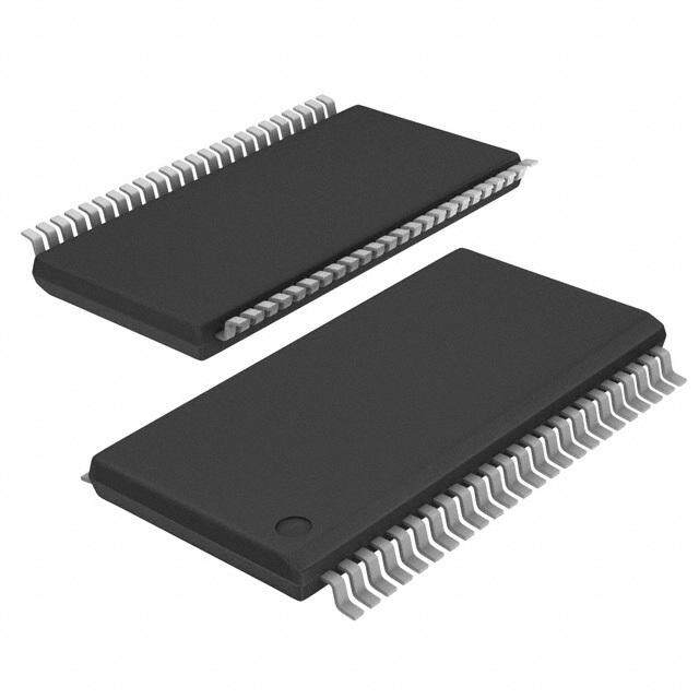
| 描述 | IC BUFF/DVR TRI-ST DUAL 20TSSOP缓冲器和线路驱动器 Octal Buffer/Driver With 3-State Outputs |
| 产品分类 | |
| 品牌 | Texas Instruments |
| 产品手册 | |
| 产品图片 |
|
| rohs | 符合RoHS无铅 / 符合限制有害物质指令(RoHS)规范要求 |
| 产品系列 | 逻辑集成电路,缓冲器和线路驱动器,Texas Instruments SN74ACT244PW74ACT |
| 数据手册 | |
| 产品型号 | SN74ACT244PW |
| 产品种类 | 缓冲器和线路驱动器 |
| 传播延迟时间 | 9 ns at 5 V |
| 低电平输出电流 | 24 mA |
| 供应商器件封装 | 20-TSSOP |
| 元件数 | 2 |
| 其它名称 | 296-26382-5 |
| 包装 | 管件 |
| 单位重量 | 77 mg |
| 商标 | Texas Instruments |
| 安装类型 | 表面贴装 |
| 安装风格 | SMD/SMT |
| 封装 | Tube |
| 封装/外壳 | 20-TSSOP(0.173",4.40mm 宽) |
| 封装/箱体 | TSSOP-20 |
| 工作温度 | -40°C ~ 85°C |
| 工厂包装数量 | 70 |
| 最大工作温度 | + 85 C |
| 最小工作温度 | - 40 C |
| 极性 | Non-Inverting |
| 标准包装 | 70 |
| 每元件位数 | 4 |
| 每芯片的通道数量 | 8 |
| 电压-电源 | 4.5 V ~ 5.5 V |
| 电流-输出高,低 | 24mA,24mA |
| 电源电压-最大 | 5.5 V |
| 电源电压-最小 | 4.5 V |
| 电源电流 | 0.04 mA |
| 系列 | SN74ACT244 |
| 输入线路数量 | 8 |
| 输出类型 | 3-State |
| 输出线路数量 | 8 |
| 逻辑类型 | 缓冲器/线路驱动器,非反相 |
| 逻辑系列 | ACT |
| 高电平输出电流 | - 24 mA |


- 商务部:美国ITC正式对集成电路等产品启动337调查
- 曝三星4nm工艺存在良率问题 高通将骁龙8 Gen1或转产台积电
- 太阳诱电将投资9.5亿元在常州建新厂生产MLCC 预计2023年完工
- 英特尔发布欧洲新工厂建设计划 深化IDM 2.0 战略
- 台积电先进制程称霸业界 有大客户加持明年业绩稳了
- 达到5530亿美元!SIA预计今年全球半导体销售额将创下新高
- 英特尔拟将自动驾驶子公司Mobileye上市 估值或超500亿美元
- 三星加码芯片和SET,合并消费电子和移动部门,撤换高东真等 CEO
- 三星电子宣布重大人事变动 还合并消费电子和移动部门
- 海关总署:前11个月进口集成电路产品价值2.52万亿元 增长14.8%


PDF Datasheet 数据手册内容提取
Product Sample & Technical Tools & Support & Folder Buy Documents Software Community SN54ACT244,SN74ACT244 SCAS517D–JUNE1995–REVISEDAUGUST2016 SNx4ACT244 Octal Buffers and Drivers With 3-State Outputs 1 Features 3 Description • 4.5-Vto5.5-VV Operation These SNx4ACT244 octal buffers and drivers are 1 CC designed specifically to improve the performance and • InputsAcceptVoltagesto5.5V density of 3-state memory address drivers, clock • Maxtpdof9.5nsat5V drivers,andbus-orientedreceiversandtransmitters. • InputsareTTLCompatible The SNx4ACT244 devices are organized as two 4-bit • OnProductsComplianttoMIL-PRF-38535, buffers and drivers with separate output-enable (OE) AllParametersareTestedUnlessOtherwise inputs. When OE is low, the device passes non- Noted.OnAllOtherProducts,Production inverted data from the A inputs to the Y outputs. ProcessingDoesNotNecessarilyIncludeTesting When OE is high, the outputs are in the high- ofAllParameters. impedancestate. DeviceInformation(1) 2 Applications PARTNUMBER PACKAGE BODYSIZE(NOM) • LEDdisplays SN74ACT244DB SSOP(20) 7.20mm×5.30mm • ServersandTelecommunication 12.80mm×7.50 SN74ACT244DW SOIC(20) • SwitchingNetworks mm 24.33mm×6.35 SN74ACT244N PDIP(20) mm 12.60mm×7.80 SN74ACT244NS SO(20) mm SN74ACT244PW TSSOP(20) 6.50mm×6.40mm SNJ54ACT244FK LCCC(20) 8.89mm×8.89mm 24.20mm×6.92 SNJ54ACT244J CDIP(20) mm (1) For all available packages, see the orderable addendum at theendofthedatasheet. LogicDiagram(PositiveLogic) 1 19 1OE 2OE 2 18 11 9 1A1 1Y1 2A1 2Y1 4 16 13 7 1A2 1Y2 2A2 2Y2 6 14 15 5 1A3 1Y3 2A3 2Y3 8 12 17 3 1A4 1Y4 2A4 2Y4 Copyright © 2016,Texas Instruments Incorporated 1 An IMPORTANT NOTICE at the end of this data sheet addresses availability, warranty, changes, use in safety-critical applications, intellectualpropertymattersandotherimportantdisclaimers.PRODUCTIONDATA.
SN54ACT244,SN74ACT244 SCAS517D–JUNE1995–REVISEDAUGUST2016 www.ti.com Table of Contents 1 Features.................................................................. 1 8.3 FeatureDescription...................................................9 2 Applications........................................................... 1 8.4 DeviceFunctionalModes..........................................9 3 Description............................................................. 1 9 ApplicationandImplementation........................ 10 4 RevisionHistory..................................................... 2 9.1 ApplicationInformation............................................10 9.2 TypicalApplication .................................................10 5 PinConfigurationandFunctions......................... 3 10 PowerSupplyRecommendations..................... 12 6 Specifications......................................................... 4 11 Layout................................................................... 12 6.1 AbsoluteMaximumRatings......................................4 6.2 ESDRatings..............................................................4 11.1 LayoutGuidelines.................................................12 6.3 RecommendedOperatingConditions.......................4 11.2 LayoutExample....................................................12 6.4 ThermalInformation..................................................5 12 DeviceandDocumentationSupport................. 13 6.5 ElectricalCharacteristics...........................................5 12.1 DocumentationSupport........................................13 6.6 SwitchingCharacteristics..........................................6 12.2 RelatedLinks........................................................13 6.7 OperatingCharacteristics..........................................6 12.3 ReceivingNotificationofDocumentationUpdates13 6.8 TypicalCharacteristics..............................................7 12.4 CommunityResources..........................................13 7 ParameterMeasurementInformation..................8 12.5 Trademarks...........................................................13 12.6 ElectrostaticDischargeCaution............................13 8 DetailedDescription.............................................. 9 12.7 Glossary................................................................13 8.1 Overview...................................................................9 13 Mechanical,Packaging,andOrderable 8.2 FunctionalBlockDiagram.........................................9 Information........................................................... 13 4 Revision History NOTE:Pagenumbersforpreviousrevisionsmaydifferfrompagenumbersinthecurrentversion. ChangesfromRevisionC(October2002)toRevisionD Page • AddedESDRatingstable,FeatureDescriptionsection,DeviceFunctionalModes,ApplicationandImplementation section,PowerSupplyRecommendationssection,Layoutsection,DeviceandDocumentationSupportsection,and Mechanical,Packaging,andOrderableInformationsection ................................................................................................. 1 2 SubmitDocumentationFeedback Copyright©1995–2016,TexasInstrumentsIncorporated ProductFolderLinks:SN54ACT244 SN74ACT244
SN54ACT244,SN74ACT244 www.ti.com SCAS517D–JUNE1995–REVISEDAUGUST2016 5 Pin Configuration and Functions SN54ACT244:JorWPackages 20-PinCDIPorCFP SN74ACT244:DB,DW,N,NS,orPWPackages TopView 20-PinSSOP,SOIC,PDIP,SO,orTSSOP TopView 11OAE1 12 2109 V2OCCE 1OE 1 20 VCC 1A1 2 19 2OE 2Y4 3 18 1Y1 2Y4 3 18 1Y1 1A2 4 17 2A4 1A2 4 17 2A4 2Y3 5 16 1Y2 2Y3 5 16 1Y2 1A3 6 15 2A3 1A3 6 15 2A3 2Y2 7 14 1Y3 2Y2 7 14 1Y3 1A4 8 13 2A2 1A4 8 13 2A2 2Y1 9 12 1Y4 2Y1 9 12 1Y4 GND 10 11 2A1 GND 10 11 2A1 SN54ACT244:FKPackage 20-PinLCCC TopView 4 1E CE Y AO CO 2 11V 2 3 2 1 20 19 1A2 4 18 1Y1 2Y3 5 17 2A4 1A3 6 16 1Y2 2Y2 7 15 2A3 1A4 8 14 1Y3 9 10 11 12 13 1 D 142 Y N AYA 2 G 212 PinFunctions PIN I/O DESCRIPTION NO. NAME 1 1OE I 1ActivelowOutputenable 2 1A1 I 1A1input 3 2Y4 O 2Y4output 4 1A2 I 1A2input 5 2Y3 O 2Y3Output 6 1A3 I 1A3input 7 2Y2 O 2Y2Output 8 1A4 I 1A4input 9 2Y1 O 2Y1Output 10 GND — Ground 11 2A1 I 2A1input 12 1Y4 O 1Y4output 13 2A2 I 2A2input 14 1Y3 O 1Y3Output 15 2A3 I 2A3input 16 1Y2 O 1Y2Output 17 2A4 I 2A4input 18 1Y1 O 1Y1Output Copyright©1995–2016,TexasInstrumentsIncorporated SubmitDocumentationFeedback 3 ProductFolderLinks:SN54ACT244 SN74ACT244
SN54ACT244,SN74ACT244 SCAS517D–JUNE1995–REVISEDAUGUST2016 www.ti.com PinFunctions(continued) PIN I/O DESCRIPTION NO. NAME 19 2OE I 2ActivelowOutputenable 20 V — Power CC 6 Specifications 6.1 Absolute Maximum Ratings overoperatingfree-airtemperaturerange(unlessotherwisenoted)(1) MIN MAX UNIT V Supplyvoltage –0.5 7 V CC V Inputvoltage(2) –0.5 V +0.5 V I CC V Outputvoltage(2) –0.5 V +0.5 V O CC I Inputclampcurrent V <0orV >V ±20 mA IK I I CC I Outputclampcurrent V <0orV >V ±20 mA OK O O CC I Continuousoutputcurrent V =0toV ±50 mA O O CC ContinuouscurrentthroughV orGND ±200 mA CC T AbsoluteMaximumJunctionTemperature 150 °C J T Storagetemperature –65 150 °C stg (1) StressesbeyondthoselistedunderAbsoluteMaximumRatingsmaycausepermanentdamagetothedevice.Thesearestressratings only,andfunctionaloperationofthedeviceattheseoranyotherconditionsbeyondthoseindicatedunderRecommendedOperating Conditionsisnotimplied.Exposuretoabsolute-maximum-ratedconditionsforextendedperiodsmayaffectdevicereliability. (2) Theinputandoutputvoltageratingsmaybeexceedediftheinputandoutputcurrentratingsareobserved. 6.2 ESD Ratings VALUE UNIT SN74ACT244inDWPackage Human-bodymodel(HBM),perANSI/ESDA/JEDECJS-001(1) ±3000 V(ESD) Electrostaticdischarge Charged-devicemodel(CDM),perJEDECspecificationJESD22- V C101(2) ±2000 SN54ACT244inJ,W,DB,N,NS,PW,FKPackages V Electrostaticdischarge Human-bodymodel(HBM),perANSI/ESDA/JEDECJS-001(1) ±2000 V (ESD) (1) JEDECdocumentJEP155statesthat500-VHBMallowssafemanufacturingwithastandardESDcontrolprocess. (2) JEDECdocumentJEP157statesthat250-VCDMallowssafemanufacturingwithastandardESDcontrolprocess. 6.3 Recommended Operating Conditions overoperatingfree-airtemperaturerange(unlessotherwisenoted)(1) MIN MAX UNIT V Supplyvoltage 4.5 5.5 V CC V High-levelinputvoltage 2 V IH V Low-levelinputvoltage 0.8 V IL V Inputvoltage 0 V V I CC V Outputvoltage 0 V V O CC I High-leveloutputcurrent –24 mA OH I Low-leveloutputcurrent 24 mA OL Δt/Δv Inputtransitionriseorfallrate 8 ns/V SN54ACT244 –55 125 T Operatingfree-airtemperature °C A SN74ACT244 –40 85 (1) AllunusedinputsofthedevicemustbeheldatV orGNDtoensureproperdeviceoperation.SeetheTIapplicationreport, CC ImplicationsofSloworFloatingCMOSInputs(SCBA004). 4 SubmitDocumentationFeedback Copyright©1995–2016,TexasInstrumentsIncorporated ProductFolderLinks:SN54ACT244 SN74ACT244
SN54ACT244,SN74ACT244 www.ti.com SCAS517D–JUNE1995–REVISEDAUGUST2016 6.4 Thermal Information SN74ACT244 THERMALMETRIC(1) DB DW N NS PW UNIT (SSOP) (SOIC) (PDIP) (SO) (TSSOP) 20PINS 20PINS 20PINS 20PINS 20PINS R Junction-to-ambientthermalresistance 94.1 81.4 48.1 76.4 103 °C/W θJA Junction-to-case(top)thermal R 55.6 46.8 34.1 42.6 37.7 °C/W θJC(top) resistance R Junction-to-boardthermalresistance 49.3 49.3 29 43.9 54 °C/W θJB Junction-to-topcharacterization ψ 20.8 20 19.5 18.8 2.8 °C/W JT parameter Junction-to-boardcharacterization ψ 48.9 48.8 28.9 43.5 53.5 °C/W JB parameter (1) Formoreinformationabouttraditionalandnewthermalmetrics,seetheSemiconductorandICPackageThermalMetricsapplication report. 6.5 Electrical Characteristics overrecommendedoperatingfree-airtemperaturerange(unlessotherwisenoted) PARAMETER TESTCONDITIONS V MIN TYP MAX UNIT CC T =25°C 4.4 4.49 A SN54ACT244 4.5V 4.4 SN74ACT244 4.4 I =–50µA OH T =25°C 5.4 5.49 A SN54ACT244 5.5V 5.4 SN74ACT244 5.4 T =25°C 3.86 A V V OH SN54ACT244 4.5V 3.7 SN74ACT244 3.76 I =–24mA OH T =25°C 4.86 A SN54ACT244 5.5V 4.7 SN74ACT244 4.76 I =–50mA(1) SN54ACT244 5.5V 3.85 OH I =–75mA(1) SN74ACT244 5.5V 3.85 OH T =25°C 0.001 0.1 A SN54ACT244 4.5V 0.1 SN74ACT244 0.1 I =50µA OL T =25°C 0.001 0.1 A SN54ACT244 5.5V 0.1 SN74ACT244 0.1 T =25°C 0.36 A V V OL SN54ACT244 4.5V 0.5 SN74ACT244 0.44 I =24mA OL T =25°C 0.36 A SN54ACT244 5.5V 0.5 SN74ACT244 0.44 I =50mA(1) SN54ACT244 5.5V 1.65 OL I =75mA(1) SN74ACT244 5.5V 1.65 OL T =25°C ±0.25 A I V =V orGND SN54ACT244 5.5V ±5 µA OZ O CC SN74ACT244 ±2.5 (1) Notmorethanoneoutputshouldbetestedatatime,andthedurationofthetestshouldnotexceed2ms. Copyright©1995–2016,TexasInstrumentsIncorporated SubmitDocumentationFeedback 5 ProductFolderLinks:SN54ACT244 SN74ACT244
SN54ACT244,SN74ACT244 SCAS517D–JUNE1995–REVISEDAUGUST2016 www.ti.com Electrical Characteristics (continued) overrecommendedoperatingfree-airtemperaturerange(unlessotherwisenoted) PARAMETER TESTCONDITIONS V MIN TYP MAX UNIT CC T =25°C ±0.1 A I V =V orGND SN54ACT244 5.5V ±1 µA I I CC SN74ACT244 ±1 T =25°C 4 A I V =V orGND,I =0 SN54ACT244 5.5V 80 µA CC I CC O SN74ACT244 40 T =25°C 0.6 A Δ (2) Oneinputat3.4V, SN54ACT244 5.5V 1.6 mA ICC OtherinputsatGNDorV CC SN74ACT244 1.5 C V =V orGND T =25°C 5V 2.5 pF I I CC A C V =V orGND T =25°C 5V 8 pF o I CC A (2) ThisistheincreaseinsupplycurrentforeachinputthatisatoneofthespecifiedTTLvoltagelevels,ratherthan0VorV . CC 6.6 Switching Characteristics overrecommendedoperatingfree-airtemperaturerange,V =5V±0.5V(unlessotherwisenoted)(seeFigure2) CC FROM TO PARAMETER TESTCONDITIONS MIN TYP MAX UNIT (INPUT) (OUTPUT) T =25°C 2 6.5 9 A t SN54ACT244 1 10 PLH SN74ACT244 1.5 10 A Y ns T =25°C 2 7 9 A t SN54ACT244 1 10 PHL SN74ACT244 1.5 10 T =25°C 1.5 7 8.5 A t SN54ACT244 1 9.5 PZH SN74ACT244 1 9.5 OE Y ns T =25°C 2 7 9.5 A t SN54ACT244 1 11 PZL SN74ACT244 1.5 10.5 T =25°C 2 8 9.5 A t SN54ACT244 1 11 PHZ SN74ACT244 1.5 10.5 OE Y ns T =25°C 2.5 7.5 10 A t SN54ACT244 1 11.5 PLZ SN74ACT244 2 10.5 6.7 Operating Characteristics V =5V,T =25°C CC A PARAMETER TESTCONDITIONS TYP UNIT C Powerdissipationcapacitanceperbuffer/driver C =50pF, f=1MHz 45 pF pd L 6 SubmitDocumentationFeedback Copyright©1995–2016,TexasInstrumentsIncorporated ProductFolderLinks:SN54ACT244 SN74ACT244
SN54ACT244,SN74ACT244 www.ti.com SCAS517D–JUNE1995–REVISEDAUGUST2016 6.8 Typical Characteristics 5.4 5.3 VCC 5.5V 5.2 5.1 5 4.9 V) 4.8 n ( 4.7 mi 4.6 H 4.5 O V 4.4 4.3 4.2 4.1 4 3.9 3.8 -75 -65 -55 -45 -35 -25 -15 -5 IOH mA D001 Figure1.V VsI OH OH Copyright©1995–2016,TexasInstrumentsIncorporated SubmitDocumentationFeedback 7 ProductFolderLinks:SN54ACT244 SN74ACT244
SN54ACT244,SN74ACT244 SCAS517D–JUNE1995–REVISEDAUGUST2016 www.ti.com 7 Parameter Measurement Information 2×VCC FromOutput 500Ω S1 Open TEST S1 UnderTest tPLH/tPHL Open CL=50pF tPLZ/tPZL 2×VCC (see NoteA) 500Ω tPHZ/tPZH Open LOAD CIRCUIT Output 3 V Control 1.5 V 1.5 V (low-level 0 V enabling) tPZL tPLZ 3 V Output ≈V Input 1.5 V 1.5 V 0 V SW1 aavt e2fo×rVmCC1 50% VCC VOL+ 0.3 V V CC OL (see Note B) tPLH tPHL tPZH tPHZ Output 50% VCC 50% VCVCOH WSa1v aeOtf oOurtpmpeu n2t 50% VCC VOH−0.3 V VOH VOL (see Note B) ≈0 V VOLTAGEWAVEFORMS VOLTAGEWAVEFORMS NOTES: A. CLincludes probe and jig capacitance. B. Waveform 1 is for an output with internal conditions such that the output is low except when disabled by the output control. Waveform 2 is for an output with internal conditions such that the output is high except when disabled by the output control. C. Allinputpulsesaresuppliedbygeneratorshavingthefollowingcharacteristics: PRR≤1MHz,ZO= 50Ω, tr≤2.5 ns,tf≤2.5 ns. D. Theoutputsaremeasuredoneatatimewithoneinputtransitionpermeasurement. Figure2. LoadCircuitandVoltageWaveforms 8 SubmitDocumentationFeedback Copyright©1995–2016,TexasInstrumentsIncorporated ProductFolderLinks:SN54ACT244 SN74ACT244
SN54ACT244,SN74ACT244 www.ti.com SCAS517D–JUNE1995–REVISEDAUGUST2016 8 Detailed Description 8.1 Overview The SNx4ACT244 devices are buffer drivers with separate output enable inputs. The active low output enable ensure the outputs are in high impedance when high. To ensure the high-impedance state during power up or power down, OE should be tied to V through a pullup resistor; the minimum value of the resistor is determined CC bythecurrent-sinkingcapabilityofthedriver. 8.2 Functional Block Diagram 1 19 1OE 2OE 2 18 11 9 1A1 1Y1 2A1 2Y1 4 16 13 7 1A2 1Y2 2A2 2Y2 6 14 15 5 1A3 1Y3 2A3 2Y3 8 12 17 3 1A4 1Y4 2A4 2Y4 Copyright © 2016,Texas Instruments Incorporated Figure3. LogicDiagram(PositiveLogic) 8.3 Feature Description The SNx4ACT244 devices are recommended for 4.5 V to 5.5-V V range under normal operating conditions. CC TheinputsareTTLcompatibleaccepting2-Vminimumhighat5-VV . CC 8.4 Device Functional Modes Table1liststhefunctionsofthedevice. Table1.FunctionTable(EachBuffer) INPUTS OUTPUT OE A Y L H H L L L H X Hi-Z Copyright©1995–2016,TexasInstrumentsIncorporated SubmitDocumentationFeedback 9 ProductFolderLinks:SN54ACT244 SN74ACT244
SN54ACT244,SN74ACT244 SCAS517D–JUNE1995–REVISEDAUGUST2016 www.ti.com 9 Application and Implementation NOTE Information in the following applications sections is not part of the TI component specification, and TI does not warrant its accuracy or completeness. TI’s customers are responsible for determining suitability of components for their purposes. Customers should validateandtesttheirdesignimplementationtoconfirmsystemfunctionality. 9.1 Application Information The SNx4ACT244 is high-drive buffer drivers providing 24-mA current drive per channel at nominal operating specifications. It can be used as LED driver with appropriate current-limiting resistors to ground or V withing CC thedevice'sandLED'soperatingcharacteristics. 9.2 Typical Application Vcc Control signal 1k(cid:13) LED SNx4ACT244 Vcc Vcc Control signal 1k(cid:13) LED SNx4ACT244 Copyright © 2016, Texas Instruments Incorporated Figure4. TypicalLEDdrivingapplication 9.2.1 DesignRequirements The pullup and pulldown current limiting resistors are chosen to operate within the LED and the SNx4ACT244 deviceoperatingspecifications.A1-kΩresistor,limitsthecurrenttolessthan5mAat5-VV operation. CC 9.2.2 DetailedDesignProcedure 1. Recommendedinputconditions: – ForthespecifiedhighandlowlevelsSee(V andV )intheRecommendedOperatingConditions. IH IL – InputsarenotovervoltagetolerantandmustbelimitedtoV . CC 2. Recommendedoutputconditions: – LimittheoutputvoltagetoV . CC – Choose the current-limiting resistor for the LED to limit the output current to I as per the O RecommendedOperatingConditions. 10 SubmitDocumentationFeedback Copyright©1995–2016,TexasInstrumentsIncorporated ProductFolderLinks:SN54ACT244 SN74ACT244
SN54ACT244,SN74ACT244 www.ti.com SCAS517D–JUNE1995–REVISEDAUGUST2016 Typical Application (continued) 9.2.3 ApplicationCurve 1.7 1.6 VCC 5.5V 1.5 1.4 1.3 1.2 V) 1.1 x ( 1 ma 0.9 V OL 00..78 0.6 0.5 0.4 0.3 0.2 0.1 0 5 10 15 20 25 30 35 40 45 50 55 60 65 70 75 IOL (mA) D001 Figure5.V vsI OL OL Copyright©1995–2016,TexasInstrumentsIncorporated SubmitDocumentationFeedback 11 ProductFolderLinks:SN54ACT244 SN74ACT244
SN54ACT244,SN74ACT244 SCAS517D–JUNE1995–REVISEDAUGUST2016 www.ti.com 10 Power Supply Recommendations The power supply may be any voltage between the MIN and MAX supply voltage rating located in the RecommendedOperatingConditions. Each V terminal should have a good bypass capacitor to prevent power disturbance. A 0.1-µF capacitor is CC recommended for devices with a single supply. If there are multiple V terminals, then 0.01-µF or 0.022-µF CC capacitors are recommended for each power terminal. It is permissible to parallel multiple bypass capacitors to reject different frequencies of noise. Multiple bypass capacitors may be paralleled to reject different frequencies ofnoise.Thebypasscapacitorshouldbeinstalledasclosetothepowerterminalaspossibleforthebestresults. 11 Layout 11.1 Layout Guidelines Inputs should not float when using multiple bit logic devices. In many cases, functions or parts of functions of digital logic devices are unused. Some examples include situations when only two inputs of a triple-input AND gate are used, or when only 3 of the 4-buffer gates are used. Such input pins should not be left unconnected becausetheundefinedvoltagesattheoutsideconnectionsresultinundefinedoperationalstates. Specified in the Figure 6 are rules that must be observed under all circumstances. All unused inputs of digital logic devices must be connected to a high or low bias to prevent them from floating. The logic level that should be applied to any particular unused input depends on the function of the device. Generally, they will be tied to GNDorV ,whichevermakesmoresenseorismoreconvenient. CC 11.2 Layout Example VCC Input Unused Input Output Unused Input Output Input Figure6. LayoutExample 12 SubmitDocumentationFeedback Copyright©1995–2016,TexasInstrumentsIncorporated ProductFolderLinks:SN54ACT244 SN74ACT244
SN54ACT244,SN74ACT244 www.ti.com SCAS517D–JUNE1995–REVISEDAUGUST2016 12 Device and Documentation Support 12.1 Documentation Support 12.1.1 RelatedDocumentation Forrelateddocumentationseethefollowing: ImplicationsofSloworFloatingCMOSInputs (SCBA004). 12.2 Related Links The table below lists quick access links. Categories include technical documents, support and community resources,toolsandsoftware,andquickaccesstosampleorbuy. Table2.RelatedLinks TECHNICAL TOOLS& SUPPORT& PARTS PRODUCTFOLDER SAMPLE&BUY DOCUMENTS SOFTWARE COMMUNITY SN54ACT244 Clickhere Clickhere Clickhere Clickhere Clickhere SN74ACT244 Clickhere Clickhere Clickhere Clickhere Clickhere 12.3 Receiving Notification of Documentation Updates To receive notification of documentation updates, navigate to the device product folder on ti.com. In the upper right corner, click on Alert me to register and receive a weekly digest of any product information that has changed.Forchangedetails,reviewtherevisionhistoryincludedinanyreviseddocument. 12.4 Community Resources The following links connect to TI community resources. Linked contents are provided "AS IS" by the respective contributors. They do not constitute TI specifications and do not necessarily reflect TI's views; see TI's Terms of Use. TIE2E™OnlineCommunity TI'sEngineer-to-Engineer(E2E)Community.Createdtofostercollaboration amongengineers.Ate2e.ti.com,youcanaskquestions,shareknowledge,exploreideasandhelp solveproblemswithfellowengineers. DesignSupport TI'sDesignSupport QuicklyfindhelpfulE2Eforumsalongwithdesignsupporttoolsand contactinformationfortechnicalsupport. 12.5 Trademarks E2EisatrademarkofTexasInstruments. Allothertrademarksarethepropertyoftheirrespectiveowners. 12.6 Electrostatic Discharge Caution Thesedeviceshavelimitedbuilt-inESDprotection.Theleadsshouldbeshortedtogetherorthedeviceplacedinconductivefoam duringstorageorhandlingtopreventelectrostaticdamagetotheMOSgates. 12.7 Glossary SLYZ022—TIGlossary. Thisglossarylistsandexplainsterms,acronyms,anddefinitions. 13 Mechanical, Packaging, and Orderable Information The following pages include mechanical packaging and orderable information. This information is the most current data available for the designated devices. This data is subject to change without notice and revision of thisdocument.Forbrowserbasedversionsofthisdatasheet,refertothelefthandnavigation. Copyright©1995–2016,TexasInstrumentsIncorporated SubmitDocumentationFeedback 13 ProductFolderLinks:SN54ACT244 SN74ACT244
PACKAGE OPTION ADDENDUM www.ti.com 6-Feb-2020 PACKAGING INFORMATION Orderable Device Status Package Type Package Pins Package Eco Plan Lead/Ball Finish MSL Peak Temp Op Temp (°C) Device Marking Samples (1) Drawing Qty (2) (6) (3) (4/5) 5962-8776001M2A ACTIVE LCCC FK 20 1 TBD POST-PLATE N / A for Pkg Type -55 to 125 5962- 8776001M2A SNJ54ACT 244FK 5962-8776001MRA ACTIVE CDIP J 20 1 TBD Call TI N / A for Pkg Type -55 to 125 5962-8776001MR A SNJ54ACT244J 5962-8776001MSA ACTIVE CFP W 20 1 TBD Call TI N / A for Pkg Type -55 to 125 5962-8776001MS A SNJ54ACT244W 5962-8776001SRA ACTIVE CDIP J 20 1 TBD Call TI N / A for Pkg Type -55 to 125 5962-8776001SR A SNV54ACT244J 5962-8776001SSA ACTIVE CFP W 20 1 TBD Call TI N / A for Pkg Type -55 to 125 5962-8776001SS A SNV54ACT244W SN74ACT244DBR ACTIVE SSOP DB 20 2000 Green (RoHS NIPDAU Level-1-260C-UNLIM -40 to 85 AD244 & no Sb/Br) SN74ACT244DW ACTIVE SOIC DW 20 25 Green (RoHS NIPDAU Level-1-260C-UNLIM -40 to 85 ACT244 & no Sb/Br) SN74ACT244DWE4 ACTIVE SOIC DW 20 25 Green (RoHS NIPDAU Level-1-260C-UNLIM -40 to 85 ACT244 & no Sb/Br) SN74ACT244DWR ACTIVE SOIC DW 20 2000 Green (RoHS NIPDAU Level-1-260C-UNLIM -40 to 85 ACT244 & no Sb/Br) SN74ACT244DWRE4 ACTIVE SOIC DW 20 2000 Green (RoHS NIPDAU Level-1-260C-UNLIM -40 to 85 ACT244 & no Sb/Br) SN74ACT244DWRG4 ACTIVE SOIC DW 20 2000 Green (RoHS NIPDAU Level-1-260C-UNLIM -40 to 85 ACT244 & no Sb/Br) SN74ACT244N ACTIVE PDIP N 20 20 Pb-Free NIPDAU N / A for Pkg Type -40 to 85 SN74ACT244N (RoHS) SN74ACT244NE4 ACTIVE PDIP N 20 20 Pb-Free NIPDAU N / A for Pkg Type -40 to 85 SN74ACT244N (RoHS) SN74ACT244NSR ACTIVE SO NS 20 2000 Green (RoHS NIPDAU Level-1-260C-UNLIM -40 to 85 ACT244 & no Sb/Br) Addendum-Page 1
PACKAGE OPTION ADDENDUM www.ti.com 6-Feb-2020 Orderable Device Status Package Type Package Pins Package Eco Plan Lead/Ball Finish MSL Peak Temp Op Temp (°C) Device Marking Samples (1) Drawing Qty (2) (6) (3) (4/5) SN74ACT244NSRG4 ACTIVE SO NS 20 2000 Green (RoHS NIPDAU Level-1-260C-UNLIM -40 to 85 ACT244 & no Sb/Br) SN74ACT244PW ACTIVE TSSOP PW 20 70 Green (RoHS NIPDAU Level-1-260C-UNLIM -40 to 85 AD244 & no Sb/Br) SN74ACT244PWE4 ACTIVE TSSOP PW 20 70 Green (RoHS NIPDAU Level-1-260C-UNLIM -40 to 85 AD244 & no Sb/Br) SN74ACT244PWG4 ACTIVE TSSOP PW 20 70 Green (RoHS NIPDAU Level-1-260C-UNLIM -40 to 85 AD244 & no Sb/Br) SN74ACT244PWR ACTIVE TSSOP PW 20 2000 Green (RoHS NIPDAU | SN Level-1-260C-UNLIM -40 to 85 AD244 & no Sb/Br) SN74ACT244PWRE4 ACTIVE TSSOP PW 20 2000 Green (RoHS NIPDAU Level-1-260C-UNLIM -40 to 85 AD244 & no Sb/Br) SN74ACT244PWRG4 ACTIVE TSSOP PW 20 2000 Green (RoHS NIPDAU Level-1-260C-UNLIM -40 to 85 AD244 & no Sb/Br) SNJ54ACT244FK ACTIVE LCCC FK 20 1 TBD POST-PLATE N / A for Pkg Type -55 to 125 5962- 8776001M2A SNJ54ACT 244FK SNJ54ACT244J ACTIVE CDIP J 20 1 TBD Call TI N / A for Pkg Type -55 to 125 5962-8776001MR A SNJ54ACT244J SNJ54ACT244W ACTIVE CFP W 20 1 TBD Call TI N / A for Pkg Type -55 to 125 5962-8776001MS A SNJ54ACT244W (1) The marketing status values are defined as follows: ACTIVE: Product device recommended for new designs. LIFEBUY: TI has announced that the device will be discontinued, and a lifetime-buy period is in effect. NRND: Not recommended for new designs. Device is in production to support existing customers, but TI does not recommend using this part in a new design. PREVIEW: Device has been announced but is not in production. Samples may or may not be available. OBSOLETE: TI has discontinued the production of the device. (2) RoHS: TI defines "RoHS" to mean semiconductor products that are compliant with the current EU RoHS requirements for all 10 RoHS substances, including the requirement that RoHS substance do not exceed 0.1% by weight in homogeneous materials. Where designed to be soldered at high temperatures, "RoHS" products are suitable for use in specified lead-free processes. TI may reference these types of products as "Pb-Free". RoHS Exempt: TI defines "RoHS Exempt" to mean products that contain lead but are compliant with EU RoHS pursuant to a specific EU RoHS exemption. Green: TI defines "Green" to mean the content of Chlorine (Cl) and Bromine (Br) based flame retardants meet JS709B low halogen requirements of <=1000ppm threshold. Antimony trioxide based flame retardants must also meet the <=1000ppm threshold requirement. Addendum-Page 2
PACKAGE OPTION ADDENDUM www.ti.com 6-Feb-2020 (3) MSL, Peak Temp. - The Moisture Sensitivity Level rating according to the JEDEC industry standard classifications, and peak solder temperature. (4) There may be additional marking, which relates to the logo, the lot trace code information, or the environmental category on the device. (5) Multiple Device Markings will be inside parentheses. Only one Device Marking contained in parentheses and separated by a "~" will appear on a device. If a line is indented then it is a continuation of the previous line and the two combined represent the entire Device Marking for that device. (6) Lead/Ball Finish - Orderable Devices may have multiple material finish options. Finish options are separated by a vertical ruled line. Lead/Ball Finish values may wrap to two lines if the finish value exceeds the maximum column width. Important Information and Disclaimer:The information provided on this page represents TI's knowledge and belief as of the date that it is provided. TI bases its knowledge and belief on information provided by third parties, and makes no representation or warranty as to the accuracy of such information. Efforts are underway to better integrate information from third parties. TI has taken and continues to take reasonable steps to provide representative and accurate information but may not have conducted destructive testing or chemical analysis on incoming materials and chemicals. TI and TI suppliers consider certain information to be proprietary, and thus CAS numbers and other limited information may not be available for release. In no event shall TI's liability arising out of such information exceed the total purchase price of the TI part(s) at issue in this document sold by TI to Customer on an annual basis. OTHER QUALIFIED VERSIONS OF SN54ACT244, SN54ACT244-SP, SN74ACT244 : •Catalog: SN74ACT244, SN54ACT244 •Automotive: SN74ACT244-Q1, SN74ACT244-Q1 •Enhanced Product: SN74ACT244-EP, SN74ACT244-EP •Military: SN54ACT244 •Space: SN54ACT244-SP NOTE: Qualified Version Definitions: •Catalog - TI's standard catalog product •Automotive - Q100 devices qualified for high-reliability automotive applications targeting zero defects •Enhanced Product - Supports Defense, Aerospace and Medical Applications Addendum-Page 3
PACKAGE OPTION ADDENDUM www.ti.com 6-Feb-2020 •Military - QML certified for Military and Defense Applications •Space - Radiation tolerant, ceramic packaging and qualified for use in Space-based application Addendum-Page 4
PACKAGE MATERIALS INFORMATION www.ti.com 14-May-2020 TAPE AND REEL INFORMATION *Alldimensionsarenominal Device Package Package Pins SPQ Reel Reel A0 B0 K0 P1 W Pin1 Type Drawing Diameter Width (mm) (mm) (mm) (mm) (mm) Quadrant (mm) W1(mm) SN74ACT244DBR SSOP DB 20 2000 330.0 16.4 8.2 7.5 2.5 12.0 16.0 Q1 SN74ACT244DWR SOIC DW 20 2000 330.0 24.4 10.8 13.3 2.7 12.0 24.0 Q1 SN74ACT244NSR SO NS 20 2000 330.0 24.4 8.4 13.0 2.5 12.0 24.0 Q1 SN74ACT244PWR TSSOP PW 20 2000 330.0 16.4 6.95 7.1 1.6 8.0 16.0 Q1 SN74ACT244PWR TSSOP PW 20 2000 330.0 16.4 6.95 7.0 1.4 8.0 16.0 Q1 SN74ACT244PWRG4 TSSOP PW 20 2000 330.0 16.4 6.95 7.0 1.4 8.0 16.0 Q1 PackMaterials-Page1
PACKAGE MATERIALS INFORMATION www.ti.com 14-May-2020 *Alldimensionsarenominal Device PackageType PackageDrawing Pins SPQ Length(mm) Width(mm) Height(mm) SN74ACT244DBR SSOP DB 20 2000 367.0 367.0 38.0 SN74ACT244DWR SOIC DW 20 2000 367.0 367.0 45.0 SN74ACT244NSR SO NS 20 2000 367.0 367.0 45.0 SN74ACT244PWR TSSOP PW 20 2000 364.0 364.0 27.0 SN74ACT244PWR TSSOP PW 20 2000 367.0 367.0 38.0 SN74ACT244PWRG4 TSSOP PW 20 2000 367.0 367.0 38.0 PackMaterials-Page2
None
None
PACKAGE OUTLINE DB0020A SSOP - 2 mm max height SCALE 2.000 SMALL OUTLINE PACKAGE C 8.2 TYP 7.4 A 0.1 C PIN 1 INDEX AREA SEATING PLANE 18X 0.65 20 1 2X 7.5 5.85 6.9 NOTE 3 10 11 0.38 20X 0.22 5.6 B 0.1 C A B 5.0 NOTE 4 2 MAX (0.15) TYP 0.25 SEE DETAIL A GAGE PLANE 0 -8 0.95 0.05 MIN 0.55 DETA 15AIL A TYPICAL 4214851/B 08/2019 NOTES: 1. All linear dimensions are in millimeters. Any dimensions in parenthesis are for reference only. Dimensioning and tolerancing per ASME Y14.5M. 2. This drawing is subject to change without notice. 3. This dimension does not include mold flash, protrusions, or gate burrs. Mold flash, protrusions, or gate burrs shall not exceed 0.15 mm per side. 4. This dimension does not include interlead flash. Interlead flash shall not exceed 0.25 mm per side. 5. Reference JEDEC registration MO-150. www.ti.com
EXAMPLE BOARD LAYOUT DB0020A SSOP - 2 mm max height SMALL OUTLINE PACKAGE 20X (1.85) SYMM (R0.05) TYP 1 20X (0.45) 20 SYMM 18X (0.65) 10 11 (7) LAND PATTERN EXAMPLE EXPOSED METAL SHOWN SCALE: 10X SOLDER MASK METAL METAL UNDER SOLDER MASK OPENING SOLDER MASK OPENING EXPOSED METAL EXPOSED METAL 0.07 MAX 0.07 MIN ALL AROUND ALL AROUND NON-SOLDER MASK SOLDER MASK DEFINED DEFINED (PREFERRED) SOLDE15.000 R MASK DETAILS 4214851/B 08/2019 NOTES: (continued) 6. Publication IPC-7351 may have alternate designs. 7. Solder mask tolerances between and around signal pads can vary based on board fabrication site. www.ti.com
EXAMPLE STENCIL DESIGN DB0020A SSOP - 2 mm max height SMALL OUTLINE PACKAGE 20X (1.85) SYMM (R0.05) TYP 1 20X (0.45) 20 SYMM 18X (0.65) 10 11 (7) SOLDER PASTE EXAMPLE BASED ON 0.125 mm THICK STENCIL SCALE: 10X 4214851/B 08/2019 NOTES: (continued) 8. Laser cutting apertures with trapezoidal walls and rounded corners may offer better paste release. IPC-7525 may have alternate design recommendations. 9. Board assembly site may have different recommendations for stencil design. www.ti.com
None
None
None
None
None
PACKAGE OUTLINE DW0020A SOIC - 2.65 mm max height SCALE 1.200 SOIC C 10.63 SEATING PLANE TYP 9.97 A PIN 1 ID 0.1 C AREA 18X 1.27 20 1 13.0 2X 12.6 11.43 NOTE 3 10 11 0.51 20X 7.6 0.31 2.65 MAX B 7.4 0.25 C A B NOTE 4 0.33 TYP 0.10 0.25 SEE DETAIL A GAGE PLANE 0.3 1.27 0 - 8 0.1 0.40 DETAIL A TYPICAL 4220724/A 05/2016 NOTES: 1. All linear dimensions are in millimeters. Dimensions in parenthesis are for reference only. Dimensioning and tolerancing per ASME Y14.5M. 2. This drawing is subject to change without notice. 3. This dimension does not include mold flash, protrusions, or gate burrs. Mold flash, protrusions, or gate burrs shall not exceed 0.15 mm per side. 4. This dimension does not include interlead flash. Interlead flash shall not exceed 0.43 mm per side. 5. Reference JEDEC registration MS-013. www.ti.com
EXAMPLE BOARD LAYOUT DW0020A SOIC - 2.65 mm max height SOIC 20X (2) SYMM 1 20 20X (0.6) 18X (1.27) SYMM (R0.05) TYP 10 11 (9.3) LAND PATTERN EXAMPLE SCALE:6X SOOPLEDNEINRG MASK METAL MSOELTDAEL RU NMDAESRK SOOPLEDNEINRG MASK 0.07 MAX 0.07 MIN ALL AROUND ALL AROUND NON SOLDER MASK SOLDER MASK DEFINED DEFINED SOLDER MASK DETAILS 4220724/A 05/2016 NOTES: (continued) 6. Publication IPC-7351 may have alternate designs. 7. Solder mask tolerances between and around signal pads can vary based on board fabrication site. www.ti.com
EXAMPLE STENCIL DESIGN DW0020A SOIC - 2.65 mm max height SOIC 20X (2) SYMM 1 20 20X (0.6) 18X (1.27) SYMM 10 11 (9.3) SOLDER PASTE EXAMPLE BASED ON 0.125 mm THICK STENCIL SCALE:6X 4220724/A 05/2016 NOTES: (continued) 8. Laser cutting apertures with trapezoidal walls and rounded corners may offer better paste release. IPC-7525 may have alternate design recommendations. 9. Board assembly site may have different recommendations for stencil design. www.ti.com
IMPORTANTNOTICEANDDISCLAIMER TI PROVIDES TECHNICAL AND RELIABILITY DATA (INCLUDING DATASHEETS), DESIGN RESOURCES (INCLUDING REFERENCE DESIGNS), APPLICATION OR OTHER DESIGN ADVICE, WEB TOOLS, SAFETY INFORMATION, AND OTHER RESOURCES “AS IS” AND WITH ALL FAULTS, AND DISCLAIMS ALL WARRANTIES, EXPRESS AND IMPLIED, INCLUDING WITHOUT LIMITATION ANY IMPLIED WARRANTIES OF MERCHANTABILITY, FITNESS FOR A PARTICULAR PURPOSE OR NON-INFRINGEMENT OF THIRD PARTY INTELLECTUAL PROPERTY RIGHTS. These resources are intended for skilled developers designing with TI products. You are solely responsible for (1) selecting the appropriate TI products for your application, (2) designing, validating and testing your application, and (3) ensuring your application meets applicable standards, and any other safety, security, or other requirements. These resources are subject to change without notice. TI grants you permission to use these resources only for development of an application that uses the TI products described in the resource. Other reproduction and display of these resources is prohibited. No license is granted to any other TI intellectual property right or to any third party intellectual property right. TI disclaims responsibility for, and you will fully indemnify TI and its representatives against, any claims, damages, costs, losses, and liabilities arising out of your use of these resources. TI’s products are provided subject to TI’s Terms of Sale (www.ti.com/legal/termsofsale.html) or other applicable terms available either on ti.com or provided in conjunction with such TI products. TI’s provision of these resources does not expand or otherwise alter TI’s applicable warranties or warranty disclaimers for TI products. Mailing Address: Texas Instruments, Post Office Box 655303, Dallas, Texas 75265 Copyright © 2020, Texas Instruments Incorporated