ICGOO在线商城 > 集成电路(IC) > 逻辑 - 缓冲器,驱动器,接收器,收发器 > SN7407NSRE4
 Datasheet下载
- 型号: SN7407NSRE4
- 制造商: Texas Instruments
- 库位|库存: xxxx|xxxx
- 要求:
| 数量阶梯 | 香港交货 | 国内含税 |
| +xxxx | $xxxx | ¥xxxx |
查看当月历史价格
查看今年历史价格
SN7407NSRE4产品简介:
ICGOO电子元器件商城为您提供SN7407NSRE4由Texas Instruments设计生产,在icgoo商城现货销售,并且可以通过原厂、代理商等渠道进行代购。 SN7407NSRE4价格参考。Texas InstrumentsSN7407NSRE4封装/规格:逻辑 - 缓冲器,驱动器,接收器,收发器, Buffer, Non-Inverting 6 Element 1 Bit per Element Open Collector Output 14-SOP。您可以下载SN7407NSRE4参考资料、Datasheet数据手册功能说明书,资料中有SN7407NSRE4 详细功能的应用电路图电压和使用方法及教程。
SN7407NSRE4 是 Texas Instruments 生产的一款逻辑缓冲器,属于 74 系列器件。它主要用于信号转换和驱动能力增强,特别适用于需要将 TTL(晶体管-晶体管逻辑)电平转换为开放集电极输出的应用场景。以下是该型号的一些典型应用场景:

1. 接口电路:SN7407NSRE4 常用于设计各种接口电路,如连接微控制器、传感器或其他数字设备。它的开放集电极输出允许与不同电压电平的系统进行通信,例如将 5V TTL 信号转换为 12V 或更高电压的信号。

2. 驱动负载:该芯片可以用来驱动外部负载,如继电器、LED 或小型电机。由于其高电流驱动能力,可以直接控制这些设备而无需额外的驱动电路。每个输出引脚可以提供高达 30mA 的电流,适合驱动低功耗设备。

3. 总线管理:在多主控系统中,SN7407NSRE4 可以帮助管理数据总线上的竞争问题。通过使用开放集电极输出,多个设备可以在同一总线上共享数据,而不会产生冲突。

4. 电平转换:当需要在不同的逻辑电平之间进行转换时,SN7407NSRE4 是一个理想的选择。它可以将低电压的 TTL 信号转换为更高的电压信号,从而兼容更多的外围设备或扩展模块。

5. 噪声抑制:开放集电极输出结构有助于减少电磁干扰 (EMI),因为它可以通过外部电阻设置适当的上升和下降时间,从而降低快速切换引起的尖峰噪声。

总之,SN7407NSRE4 在各种嵌入式系统、工业控制、自动化设备等领域有着广泛的应用,尤其适合需要灵活的信号处理和驱动能力的场合。
| 参数 | 数值 |
| 产品目录 | 集成电路 (IC)半导体 |
| 描述 | IC BUFF/DVR HEX NON-INV 14SO缓冲器和线路驱动器 Hex Buffer/Driver |
| 产品分类 | |
| 品牌 | Texas Instruments |
| 产品手册 | |
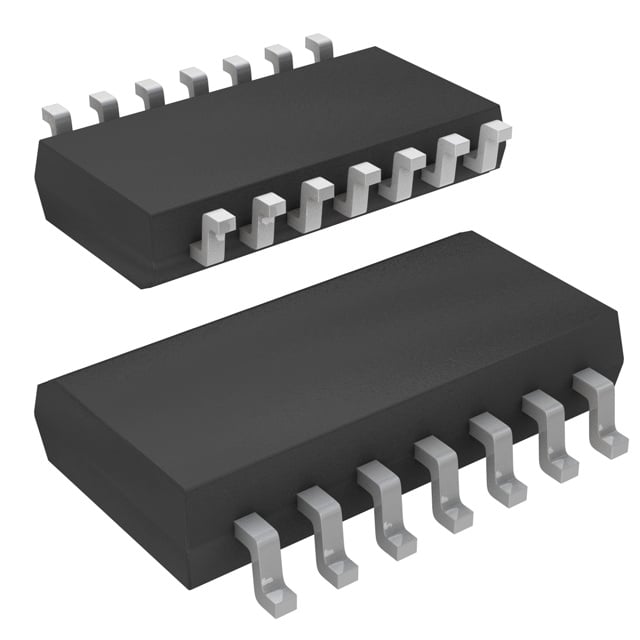
| 产品图片 |
|
| rohs | 符合RoHS无铅 / 符合限制有害物质指令(RoHS)规范要求 |
| 产品系列 | 逻辑集成电路,缓冲器和线路驱动器,Texas Instruments SN7407NSRE47400 |
| 数据手册 | |
| 产品型号 | SN7407NSRE4 |
| 产品种类 | 缓冲器和线路驱动器 |
| 传播延迟时间 | 26 ns at 5 V |
| 低电平输出电流 | 40 mA |
| 供应商器件封装 | 14-SO |
| 元件数 | 6 |
| 包装 | 带卷 (TR) |
| 单位重量 | 208.300 mg |
| 商标 | Texas Instruments |
| 安装类型 | 表面贴装 |
| 安装风格 | SMD/SMT |
| 封装 | Reel |
| 封装/外壳 | 14-SOIC(0.209",5.30mm 宽) |
| 封装/箱体 | SOP-14 |
| 工作温度 | 0°C ~ 70°C |
| 工厂包装数量 | 2000 |
| 最大功率耗散 | 145 mW |
| 最大工作温度 | + 70 C |
| 最小工作温度 | 0 C |
| 极性 | Non-Inverting |
| 标准包装 | 2,000 |
| 每元件位数 | 1 |
| 每芯片的通道数量 | 5 |
| 电压-电源 | 4.75 V ~ 5.25 V |
| 电流-输出高,低 | -,40mA |
| 电源电压-最大 | 5.25 V |
| 电源电压-最小 | 4.75 V |
| 电源电流 | 0.041 mA |
| 系列 | SN7407 |
| 输入线路数量 | 6 |
| 输出类型 | Open Collector |
| 输出线路数量 | 18 |
| 逻辑类型 | Bipolar |
| 逻辑系列 | TTL |
| 高电平输出电流 | - 0.25 mA |


- 商务部:美国ITC正式对集成电路等产品启动337调查
- 曝三星4nm工艺存在良率问题 高通将骁龙8 Gen1或转产台积电
- 太阳诱电将投资9.5亿元在常州建新厂生产MLCC 预计2023年完工
- 英特尔发布欧洲新工厂建设计划 深化IDM 2.0 战略
- 台积电先进制程称霸业界 有大客户加持明年业绩稳了
- 达到5530亿美元!SIA预计今年全球半导体销售额将创下新高
- 英特尔拟将自动驾驶子公司Mobileye上市 估值或超500亿美元
- 三星加码芯片和SET,合并消费电子和移动部门,撤换高东真等 CEO
- 三星电子宣布重大人事变动 还合并消费电子和移动部门
- 海关总署:前11个月进口集成电路产品价值2.52万亿元 增长14.8%


PDF Datasheet 数据手册内容提取
Product Sample & Technical Tools & Support & Folder Buy Documents Software Community SN5407,SN5417,SN7407,SN7417 SDLS032H–DECEMBER1983–REVISEDSEPTEMBER2016 SNx407 and SNx417 Hex Buffers and Drivers With Open-Collector High-Voltage Outputs 1 Features 3 Description • ConvertTTLVoltageLevelstoMOSLevels These TTL hex buffers and drivers feature high- 1 voltage open-collector outputs for interfacing with • HighSink-CurrentCapabilityDesign high-level circuits (such as MOS) or for driving high- • Open-CollectorDriverforIndicatorLamps current loads (such as lamps or relays), and also are • InputsFullyCompatibleWithMostTTLCircuits characterized for use as buffers for driving TTL inputs. The SN5407 and SN7407 devices have • OnProductsComplianttoMIL-PRF-38535, minimum breakdown voltages of 30 V, and the AllParametersAreTestedUnlessOtherwise SN5417 and SN7417 devices have minimum Noted.OnAllOtherProducts,Production breakdown voltages of 15 V. The maximum sink ProcessingDoesNotNecessarilyIncludeTesting currentis30mAfortheSN5407andSN5417devices ofAllParameters. and40mAfortheSN7407andSN7417devices. These devices perform the Boolean function Y = A in 2 Applications positivelogic. • AudioDocks:Portable These circuits are completely compatible with most • Blu-rayDisc®PlayersandHomeTheaters TTL families. Inputs are diode clamped to minimize • MP3PlayersorRecorders transmission-line effects, which simplifies design. • PersonalDigitalAssistants(PDAs) Typical power dissipation is 145 mW, and average propagationdelaytimeis14ns. • Power:TelecomandServerACorDCSupply: SingleControllers:AnalogandDigital DeviceInformation(1) • Solid-StateDrive(SSD):ClientandEnterprise PARTNUMBER PACKAGE BODYSIZE(NOM) • TV:LCD,Digital,andHigh-Definition(HDTV) SNx407J, CDIP(14) 19.56mm×6.92mm • Tablets:Enterprise SNx417J • VideoAnalytics:Servers SN74x7D SOIC(14) 8.65mm×3.91mm SN74x7N PDIP(14) 19.30mm×6.35mm • WirelessHeadsets,Keyboards,andMice SNJ5407FK LCCC(20) 8.89mm×8.89mm SNJ5407W CFP(14) 9.21mm×5.97mm (1) For all available packages, see the orderable addendum at theendofthedatasheet. LogicDiagram,EachBufferandDriver(PositiveLogic) A Y Copyright © 2016, Texas Instruments Incorporated 1 An IMPORTANT NOTICE at the end of this data sheet addresses availability, warranty, changes, use in safety-critical applications, intellectualpropertymattersandotherimportantdisclaimers.PRODUCTIONDATA.
SN5407,SN5417,SN7407,SN7417 SDLS032H–DECEMBER1983–REVISEDSEPTEMBER2016 www.ti.com Table of Contents 1 Features.................................................................. 1 8.4 DeviceFunctionalModes..........................................8 2 Applications........................................................... 1 9 ApplicationandImplementation.......................... 9 3 Description............................................................. 1 9.1 ApplicationInformation..............................................9 4 RevisionHistory..................................................... 2 9.2 TypicalApplication....................................................9 5 PinConfigurationandFunctions......................... 3 10 PowerSupplyRecommendations..................... 10 6 Specifications......................................................... 4 11 Layout................................................................... 10 6.1 AbsoluteMaximumRatings......................................4 11.1 LayoutGuidelines.................................................10 6.2 ESDRatings..............................................................4 11.2 LayoutExample....................................................10 6.3 RecommendedOperatingConditions.......................4 12 DeviceandDocumentationSupport................. 11 6.4 ThermalInformation..................................................5 12.1 DocumentationSupport........................................11 6.5 ElectricalCharacteristics...........................................5 12.2 RelatedLinks........................................................11 6.6 SwitchingCharacteristics..........................................5 12.3 ReceivingNotificationofDocumentationUpdates11 6.7 TypicalCharacteristics..............................................6 12.4 CommunityResources..........................................11 7 ParameterMeasurementInformation..................7 12.5 Trademarks...........................................................11 12.6 ElectrostaticDischargeCaution............................11 8 DetailedDescription.............................................. 8 12.7 Glossary................................................................11 8.1 Overview...................................................................8 13 Mechanical,Packaging,andOrderable 8.2 FunctionalBlockDiagram.........................................8 Information........................................................... 12 8.3 FeatureDescription...................................................8 4 Revision History NOTE:Pagenumbersforpreviousrevisionsmaydifferfrompagenumbersinthecurrentversion. ChangesfromRevisionG(May2004)toRevisionH Page • AddedESDRatingstable,FeatureDescriptionsection,DeviceFunctionalModes,ApplicationandImplementation section,PowerSupplyRecommendationssection,Layoutsection,DeviceandDocumentationSupportsection,and Mechanical,Packaging,andOrderableInformationsection.................................................................................................. 1 • DeletedOrderingInformationtable;seePOAattheendofthedatasheet........................................................................... 1 • AddedMilitaryDisclaimertoFeatures.................................................................................................................................... 1 • ChangedR valuesforSN7404:D(SOIC)from86to86.8,N(PDIP)from80to52.1,andNS(SO)from76to85.9...... 5 θJA 2 SubmitDocumentationFeedback Copyright©1983–2016,TexasInstrumentsIncorporated ProductFolderLinks:SN5407 SN5417 SN7407 SN7417
SN5407,SN5417,SN7407,SN7417 www.ti.com SDLS032H–DECEMBER1983–REVISEDSEPTEMBER2016 5 Pin Configuration and Functions D,N,NS,J,orWPackage FKPackage 14-PinSOIC,PDIP,CDIP,orCFP 20-PinLCCC TopView TopView 1Y 1A NC V CC 6A 1A 1 14 VCC 1Y 2 13 6A 3 2 1 0 9 2 1 2A 3 12 6Y 2A 4 18 6Y 2Y 4 11 5A NC 5 17 NC 3A 5 10 5Y 2Y 6 16 5A 3Y 6 9 4A NC 7 15 NC GND 7 8 4Y 3A 8 14 5Y 0 1 2 3 9 1 1 1 1 Not to scale Not to scale Y D C Y A 3 N N 4 4 G NC–Nointernalconnection PinFunctions PIN SOIC,PDIP, I/O DESCRIPTION NAME LCCC CDIP,CFP 1A 1 2 I Input1 1Y 2 3 O Output1 2A 3 4 I Input2 2Y 4 6 O Output2 3A 5 8 I Input3 3Y 6 9 O Output3 4A 9 13 I Input4 4Y 8 12 O Output4 5A 11 16 I Input5 5Y 10 14 O Output5 6A 13 19 I Input6 6Y 12 18 O Output6 GND 7 10 — GroundPin 1,5,7,11,15, NC — — NoConnect 17 V 14 20 — PowerPin CC Copyright©1983–2016,TexasInstrumentsIncorporated SubmitDocumentationFeedback 3 ProductFolderLinks:SN5407 SN5417 SN7407 SN7417
SN5407,SN5417,SN7407,SN7417 SDLS032H–DECEMBER1983–REVISEDSEPTEMBER2016 www.ti.com 6 Specifications 6.1 Absolute Maximum Ratings overoperatingfree-airtemperaturerange(unlessotherwisenoted)(1) MIN MAX UNIT V Supplyvoltage 7 V CC V Inputvoltage(2) 5.5 V I SN5407,SN7407 30 V Outputvoltage(2)(3) V O SN5417,SN7417 15 T Junctiontemperature 150 ºC J T Storagetemperature –65 150 ºC stg (1) StressesbeyondthoselistedunderAbsoluteMaximumRatingsmaycausepermanentdamagetothedevice.Thesearestressratings only,andfunctionaloperationofthedeviceattheseoranyotherconditionsbeyondthoseindicatedunderRecommendedOperating Conditionsisnotimplied.Exposuretoabsolute-maximum-ratedconditionsforextendedperiodsmayaffectdevicereliability. (2) AllvoltagevaluesarewithrespecttoGND. (3) ThisisthemaximumvoltagethatcansafelybeappliedtoanyoutputwhenitisintheOFFstate. 6.2 ESD Ratings VALUE UNIT SN7407ANDSN7417 Human-bodymodel(HBM),perANSI/ESDA/JEDECJS-001(1) ±2000 V Electrostaticdischarge V (ESD) Charged-devicemodel(CDM),perJEDECspecificationJESD22-C101(2) ±1000 SN5407ANDSN5417 V Electrostaticdischarge Human-bodymodel(HBM) ±2000 V (ESD) (1) JEDECdocumentJEP155statesthat500-VHBMallowssafemanufacturingwithastandardESDcontrolprocess. (2) JEDECdocumentJEP157statesthat250-VCDMallowssafemanufacturingwithastandardESDcontrolprocess. 6.3 Recommended Operating Conditions overoperatingfree-airtemperaturerange(unlessotherwisenoted)(1) MIN NOM MAX UNIT SN5407,SN5417 4.5 5 5.5 V Supplyvoltage V CC SN7407,SN7417 4.75 5 5.25 V High-levelinputvoltage 2 V IH V Low-levelinputvoltage 0.8 V IL SN5407,SN7407 30 V High-leveloutputvoltage V OH SN5417,SN7417 15 SN5407,SN5417 30 I Low-leveloutputcurrent mA OL SN7407,SN7417 40 SN5407,SN5417 –55 125 T Operatingfree-airtemperature °C A SN7407,SN7417 0 70 (1) AllunusedinputsofthedevicemustbeheldatV orGNDtoensureproperdeviceoperation.SeeImplicationsofSloworFloating CC CMOSInputs,. 4 SubmitDocumentationFeedback Copyright©1983–2016,TexasInstrumentsIncorporated ProductFolderLinks:SN5407 SN5417 SN7407 SN7417
SN5407,SN5417,SN7407,SN7417 www.ti.com SDLS032H–DECEMBER1983–REVISEDSEPTEMBER2016 6.4 Thermal Information SN7407 SN7417 THERMALMETRIC(1) D(SOIC) N(PDIP) NS(SO) D(SOIC) N(PDIP) UNIT 14PINS 14PINS 14PINS 14PINS 14PINS R Junction-to-ambientthermalresistance(2) 86.8 52.1 85.9 88.8 52.1 °C/W θJA R Junction-to-case(top)thermalresistance 47.1 39.4 43.9 50.4 39.4 °C/W θJC(top) R Junction-to-boardthermalresistance 41 32 44.7 43 32 °C/W θJB ψ Junction-to-topcharacterizationparameter 15.6 24.2 14.6 16.5 24.2 °C/W JT ψ Junction-to-boardcharacterizationparameter 40.8 31.8 44.4 42.8 31.8 °C/W JB (1) Formoreinformationabouttraditionalandnewthermalmetrics,seetheSemiconductorandICPackageThermalMetricsapplication report. (2) ThepackagethermalimpedanceiscalculatedinaccordancewithJESD51-7. 6.5 Electrical Characteristics overrecommendedoperatingfree-airtemperaturerange(unlessotherwisenoted)(1)(2) PARAMETER TESTCONDITIONS MIN TYP MAX UNIT V Inputclampvoltage V =MIN,I =–12mA –1.5 V IK CC I I =16mA 0.4 OL V =MIN, V Low-leveloutputvoltage CC I =30mA,SN5407,SN5417 0.7 V OL V =0.8V OL IL I =40mA,SN7407,SN7417 0.7 OL I High-leveloutputcurrent VCC=MIN, VOH=30V,SN5407,SN7407 0.25 mA OH VIH=2V VOH=15V,SN5417,SN7417 0.25 I Inputcurrent V =MAX,V =5.5V 1 mA I CC I I High-levelinputcurrent V =MAX,V =2.4V 40 µA IH CC IH I Low-levelinputcurrent V =MAX,V =0.4V –1.6 mA IL CC IL I High-levelsupplycurrent V =MAX 29 41 mA CCH CC I Low-levelsupplycurrent V =MAX 21 30 mA CCL CC (1) AlltypicalvaluesareatV =5V,T =25°C. CC A (2) ForconditionsshownasMINorMAX,usetheappropriatevaluespecifiedunderrecommendedoperatingconditions. 6.6 Switching Characteristics V =5V,T =25°C(seeFigure2) CC A PARAMETER FROM(INPUT) TO(OUTPUT) TESTCONDITIONS MIN TYP MAX UNIT t 6 10 PLH A Y R =110Ω,C =15pF ns L L t 20 30 PHL t 15 PLH A Y R =150Ω,C =50pF ns L L t 26 PHL Copyright©1983–2016,TexasInstrumentsIncorporated SubmitDocumentationFeedback 5 ProductFolderLinks:SN5407 SN5417 SN7407 SN7417
SN5407,SN5417,SN7407,SN7417 SDLS032H–DECEMBER1983–REVISEDSEPTEMBER2016 www.ti.com 6.7 Typical Characteristics 15 12 9 s) n t (pd 6 3 0 0 5 10 15 20 25 30 V (V) out C001 Figure1.TimeLowtoHighvsV OUT 6 SubmitDocumentationFeedback Copyright©1983–2016,TexasInstrumentsIncorporated ProductFolderLinks:SN5407 SN5417 SN7407 SN7417
SN5407,SN5417,SN7407,SN7417 www.ti.com SDLS032H–DECEMBER1983–REVISEDSEPTEMBER2016 7 Parameter Measurement Information VCC RL FromOutput Test Point UnderTest CL (see NoteA) LOAD CIRCUIT 3 V Input 1.5 V 1.5 V 0 V tPLH tPHL VOH High-Level In-Phase 1.5 V 1.5 V 1.5 V 1.5 V Pulse Output VOL tw tPHL tPLH Low-Level Out-of-Phase VOH Pulse 1.5 V 1.5 V Output 1.5 V 1.5 V VOL VOLTAGEWAVEFORMS VOLTAGEWAVEFORMS PULSE WIDTHS PROPAGATIONDELAYTIMES A. C includesprobeandjigcapacitance. L B. Intheexamplesabove,thephaserelationshipsbetweeninputsandoutputshavebeenchosenarbitrarily. C. Allinputpulsesaresuppliedbygeneratorshavingthefollowingcharacteristics:PRR≤1MHz,Z =50Ω,t ≤7ns, O r t ≤7ns. f D. Theoutputsaremeasuredoneatatime,withoneinputtransitionpermeasurement. Figure2. LoadCircuitandVoltageWaveforms Copyright©1983–2016,TexasInstrumentsIncorporated SubmitDocumentationFeedback 7 ProductFolderLinks:SN5407 SN5417 SN7407 SN7417
SN5407,SN5417,SN7407,SN7417 SDLS032H–DECEMBER1983–REVISEDSEPTEMBER2016 www.ti.com 8 Detailed Description 8.1 Overview The SN74x7 is a high sink current capable open-collector buffer. This device is high-voltage tolerant on the output of up to 30 V on the SNx407 model and 15 V on the SNx417 model. The SN74x7 is also useful for convertingTTLvoltagelevelstoMOSlevels. 8.2 Functional Block Diagram VCC 6kΩ 3.4 kΩ 1.6 kΩ InputA OutputY 100Ω 1 kΩ GND Copyright © 2016,Texas Instruments Incorporated Resistervaluesshownarenominal. Figure3. Schematic 8.3 Feature Description The SNx407 and SNx417 devices are ideal for high voltage outputs. The SNx407 device has a maximum output voltage30VandtheSNx417devicehasamaximumoutputvoltage15V. Thehighsinkcurrentisupto40mAfortheSN74x7. 8.4 Device Functional Modes Table1liststhefunctionsofthedevices. Table1.FunctionTable INPUT OUTPUT A Y H High-Z L L 8 SubmitDocumentationFeedback Copyright©1983–2016,TexasInstrumentsIncorporated ProductFolderLinks:SN5407 SN5417 SN7407 SN7417
SN5407,SN5417,SN7407,SN7417 www.ti.com SDLS032H–DECEMBER1983–REVISEDSEPTEMBER2016 9 Application and Implementation NOTE Information in the following applications sections is not part of the TI component specification, and TI does not warrant its accuracy or completeness. TI’s customers are responsible for determining suitability of components for their purposes. Customers should validateandtesttheirdesignimplementationtoconfirmsystemfunctionality. 9.1 Application Information The SN74x7 device is a high-drive, open-collector device that is used for multiple buffer-type functions. The device produces 30 mA of drive current. Therefore, this device is ideal for driving multiple inputs and for high- speedapplicationsupto100MHz.Theoutputsarehighvoltagetolerantupto30VfortheSNx407. 9.2 Typical Application Figure4. TypicalApplicationDiagram 9.2.1 DesignRequirements Avoid bus contention because it can drive currents that would exceed maximum limits. The high drive also createsfastedgesintolightloads;therefore,routingandloadconditionsmustbeconsideredtopreventringing. 9.2.2 DetailedDesignProcedure 1. RecommendedInputConditions – Risetimeandfalltimespecs:Seet andt inSwitchingCharacteristics. PHL PLH – Specifiedhighandlowlevels:SeeV andV inRecommendedOperatingConditions. IH IL 2. RecommendOutputConditions – Loadcurrentsmustnotexceed30mA. – Outputsmustnotbepulledabove30VfortheSNx407device. Copyright©1983–2016,TexasInstrumentsIncorporated SubmitDocumentationFeedback 9 ProductFolderLinks:SN5407 SN5417 SN7407 SN7417
SN5407,SN5417,SN7407,SN7417 SDLS032H–DECEMBER1983–REVISEDSEPTEMBER2016 www.ti.com Typical Application (continued) 9.2.3 ApplicationCurve 40 35 A) 30 m I (OL25 20 15 0.4 0.5 0.6 0.7 V (V) OL C002 Figure5. V vsI OL OL 10 Power Supply Recommendations The power supply can be any voltage between the minimum and maximum supply voltage rating (see RecommendedOperatingConditions). Each V pin must have a good bypass capacitor to prevent power disturbance. TI recommends 0.1 µF for CC devices with a single supply. If there are multiple V pins, then TI recommends 0.01 µF or 0.022 µF for each CC power pin. It is acceptable to parallel multiple bypass capacitors to reject different frequencies of noise. A 0.1 µF and a 1 µF are commonly used in parallel. The bypass capacitor must be installed as close to the power pin as possibleforbestresults. 11 Layout 11.1 Layout Guidelines Whenusingmultiplebitlogicdevicesinputsmustneverfloat. In many cases, functions or parts of functions of digital logic devices are unused, for example, when only two inputs of a triple-input AND gate are used or only 3 of the 4 buffer gates are used. Such input pins must not be left unconnected because the undefined voltages at the outside connections result in undefined operational states. Figure 6 specifies the rules that must be observed under all circumstances. All unused inputs of digital logic devices must be connected to a high or low bias to prevent them from floating. The logic level that must be applied to any particular unused input depends on the function of the device. Generally they are tied to GND or V , whichever makes more sense or is more convenient. It is generally acceptable to float outputs, unless the CC partisatransceiver. 11.2 Layout Example V cc Input Unused Input Output Unused Input Output Input Figure6. LayoutDiagram 10 SubmitDocumentationFeedback Copyright©1983–2016,TexasInstrumentsIncorporated ProductFolderLinks:SN5407 SN5417 SN7407 SN7417
SN5407,SN5417,SN7407,SN7417 www.ti.com SDLS032H–DECEMBER1983–REVISEDSEPTEMBER2016 12 Device and Documentation Support 12.1 Documentation Support 12.1.1 RelatedDocumentation Forrelateddocumentationseethefollowing: ImplicationsofSloworFloatingCMOSInputs, (SCBA004) 12.2 Related Links The table below lists quick access links. Categories include technical documents, support and community resources,toolsandsoftware,andquickaccesstosampleorbuy. Table2.RelatedLinks TECHNICAL TOOLS& SUPPORT& PARTS PRODUCTFOLDER SAMPLE&BUY DOCUMENTS SOFTWARE COMMUNITY SN5407 Clickhere Clickhere Clickhere Clickhere Clickhere SN5417 Clickhere Clickhere Clickhere Clickhere Clickhere SN7407 Clickhere Clickhere Clickhere Clickhere Clickhere SN7417 Clickhere Clickhere Clickhere Clickhere Clickhere 12.3 Receiving Notification of Documentation Updates To receive notification of documentation updates, navigate to the device product folder on ti.com. In the upper right corner, click on Alert meto register and receive a weekly digest of any product information that has changed.Forchangedetails,reviewtherevisionhistoryincludedinanyreviseddocument. 12.4 Community Resources The following links connect to TI community resources. Linked contents are provided "AS IS" by the respective contributors. They do not constitute TI specifications and do not necessarily reflect TI's views; see TI's Terms of Use. TIE2E™OnlineCommunity TI'sEngineer-to-Engineer(E2E)Community.Createdtofostercollaboration amongengineers.Ate2e.ti.com,youcanaskquestions,shareknowledge,exploreideasandhelp solveproblemswithfellowengineers. DesignSupport TI'sDesignSupport QuicklyfindhelpfulE2Eforumsalongwithdesignsupporttoolsand contactinformationfortechnicalsupport. 12.5 Trademarks E2EisatrademarkofTexasInstruments. Blu-rayDiscisaregisteredtrademarkofBlue-rayDiscAssociation. Allothertrademarksarethepropertyoftheirrespectiveowners. 12.6 Electrostatic Discharge Caution This integrated circuit can be damaged by ESD. Texas Instruments recommends that all integrated circuits be handled with appropriateprecautions.Failuretoobserveproperhandlingandinstallationprocedurescancausedamage. ESDdamagecanrangefromsubtleperformancedegradationtocompletedevicefailure.Precisionintegratedcircuitsmaybemore susceptibletodamagebecauseverysmallparametricchangescouldcausethedevicenottomeetitspublishedspecifications. 12.7 Glossary SLYZ022—TIGlossary. Thisglossarylistsandexplainsterms,acronyms,anddefinitions. Copyright©1983–2016,TexasInstrumentsIncorporated SubmitDocumentationFeedback 11 ProductFolderLinks:SN5407 SN5417 SN7407 SN7417
SN5407,SN5417,SN7407,SN7417 SDLS032H–DECEMBER1983–REVISEDSEPTEMBER2016 www.ti.com 13 Mechanical, Packaging, and Orderable Information The following pages include mechanical packaging and orderable information. This information is the most current data available for the designated devices. This data is subject to change without notice and revision of thisdocument.Forbrowserbasedversionsofthisdatasheet,refertothelefthandnavigation. 12 SubmitDocumentationFeedback Copyright©1983–2016,TexasInstrumentsIncorporated ProductFolderLinks:SN5407 SN5417 SN7407 SN7417
PACKAGE OPTION ADDENDUM www.ti.com 6-Feb-2020 PACKAGING INFORMATION Orderable Device Status Package Type Package Pins Package Eco Plan Lead/Ball Finish MSL Peak Temp Op Temp (°C) Device Marking Samples (1) Drawing Qty (2) (6) (3) (4/5) JM38510/00803BCA ACTIVE CDIP J 14 1 TBD Call TI N / A for Pkg Type -55 to 125 JM38510/ 00803BCA JM38510/00803BDA ACTIVE CFP W 14 1 TBD Call TI N / A for Pkg Type -55 to 125 JM38510/ 00803BDA M38510/00803BCA ACTIVE CDIP J 14 1 TBD Call TI N / A for Pkg Type -55 to 125 JM38510/ 00803BCA M38510/00803BDA ACTIVE CFP W 14 1 TBD Call TI N / A for Pkg Type -55 to 125 JM38510/ 00803BDA SN5407J ACTIVE CDIP J 14 1 TBD Call TI N / A for Pkg Type -55 to 125 SN5407J SN5417J ACTIVE CDIP J 14 1 TBD Call TI N / A for Pkg Type -55 to 125 SN5417J SN7407D ACTIVE SOIC D 14 50 Green (RoHS NIPDAU Level-1-260C-UNLIM 0 to 70 7407 & no Sb/Br) SN7407DE4 ACTIVE SOIC D 14 50 Green (RoHS NIPDAU Level-1-260C-UNLIM 0 to 70 7407 & no Sb/Br) SN7407DG4 ACTIVE SOIC D 14 50 Green (RoHS NIPDAU Level-1-260C-UNLIM 0 to 70 7407 & no Sb/Br) SN7407DR ACTIVE SOIC D 14 2500 Green (RoHS NIPDAU Level-1-260C-UNLIM 0 to 70 7407 & no Sb/Br) SN7407DRE4 ACTIVE SOIC D 14 2500 Green (RoHS NIPDAU Level-1-260C-UNLIM 0 to 70 7407 & no Sb/Br) SN7407DRG4 ACTIVE SOIC D 14 2500 Green (RoHS NIPDAU Level-1-260C-UNLIM 0 to 70 7407 & no Sb/Br) SN7407N ACTIVE PDIP N 14 25 Green (RoHS NIPDAU N / A for Pkg Type 0 to 70 SN7407N & no Sb/Br) SN7407NE4 ACTIVE PDIP N 14 25 Green (RoHS NIPDAU N / A for Pkg Type 0 to 70 SN7407N & no Sb/Br) SN7407NSR ACTIVE SO NS 14 2000 Green (RoHS NIPDAU Level-1-260C-UNLIM 0 to 70 SN7407 & no Sb/Br) SN7407NSRG4 ACTIVE SO NS 14 2000 Green (RoHS NIPDAU Level-1-260C-UNLIM 0 to 70 SN7407 & no Sb/Br) SN7417D ACTIVE SOIC D 14 50 Green (RoHS NIPDAU Level-1-260C-UNLIM 0 to 70 7417 & no Sb/Br) Addendum-Page 1
PACKAGE OPTION ADDENDUM www.ti.com 6-Feb-2020 Orderable Device Status Package Type Package Pins Package Eco Plan Lead/Ball Finish MSL Peak Temp Op Temp (°C) Device Marking Samples (1) Drawing Qty (2) (6) (3) (4/5) SN7417DR ACTIVE SOIC D 14 2500 Green (RoHS NIPDAU Level-1-260C-UNLIM 0 to 70 7417 & no Sb/Br) SN7417N ACTIVE PDIP N 14 25 Green (RoHS NIPDAU N / A for Pkg Type 0 to 70 SN7417N & no Sb/Br) SNJ5407FK ACTIVE LCCC FK 20 1 TBD POST-PLATE N / A for Pkg Type -55 to 125 SNJ5407FK SNJ5407J ACTIVE CDIP J 14 1 TBD Call TI N / A for Pkg Type -55 to 125 SNJ5407J SNJ5407W ACTIVE CFP W 14 1 TBD Call TI N / A for Pkg Type -55 to 125 SNJ5407W SNJ5417J ACTIVE CDIP J 14 1 TBD Call TI N / A for Pkg Type -55 to 125 SNJ5417J (1) The marketing status values are defined as follows: ACTIVE: Product device recommended for new designs. LIFEBUY: TI has announced that the device will be discontinued, and a lifetime-buy period is in effect. NRND: Not recommended for new designs. Device is in production to support existing customers, but TI does not recommend using this part in a new design. PREVIEW: Device has been announced but is not in production. Samples may or may not be available. OBSOLETE: TI has discontinued the production of the device. (2) RoHS: TI defines "RoHS" to mean semiconductor products that are compliant with the current EU RoHS requirements for all 10 RoHS substances, including the requirement that RoHS substance do not exceed 0.1% by weight in homogeneous materials. Where designed to be soldered at high temperatures, "RoHS" products are suitable for use in specified lead-free processes. TI may reference these types of products as "Pb-Free". RoHS Exempt: TI defines "RoHS Exempt" to mean products that contain lead but are compliant with EU RoHS pursuant to a specific EU RoHS exemption. Green: TI defines "Green" to mean the content of Chlorine (Cl) and Bromine (Br) based flame retardants meet JS709B low halogen requirements of <=1000ppm threshold. Antimony trioxide based flame retardants must also meet the <=1000ppm threshold requirement. (3) MSL, Peak Temp. - The Moisture Sensitivity Level rating according to the JEDEC industry standard classifications, and peak solder temperature. (4) There may be additional marking, which relates to the logo, the lot trace code information, or the environmental category on the device. (5) Multiple Device Markings will be inside parentheses. Only one Device Marking contained in parentheses and separated by a "~" will appear on a device. If a line is indented then it is a continuation of the previous line and the two combined represent the entire Device Marking for that device. (6) Lead/Ball Finish - Orderable Devices may have multiple material finish options. Finish options are separated by a vertical ruled line. Lead/Ball Finish values may wrap to two lines if the finish value exceeds the maximum column width. Important Information and Disclaimer:The information provided on this page represents TI's knowledge and belief as of the date that it is provided. TI bases its knowledge and belief on information provided by third parties, and makes no representation or warranty as to the accuracy of such information. Efforts are underway to better integrate information from third parties. TI has taken and Addendum-Page 2
PACKAGE OPTION ADDENDUM www.ti.com 6-Feb-2020 continues to take reasonable steps to provide representative and accurate information but may not have conducted destructive testing or chemical analysis on incoming materials and chemicals. TI and TI suppliers consider certain information to be proprietary, and thus CAS numbers and other limited information may not be available for release. In no event shall TI's liability arising out of such information exceed the total purchase price of the TI part(s) at issue in this document sold by TI to Customer on an annual basis. OTHER QUALIFIED VERSIONS OF SN5407, SN5417, SN7407, SN7417 : •Catalog: SN7407, SN7417 •Military: SN5407, SN5417 NOTE: Qualified Version Definitions: •Catalog - TI's standard catalog product •Military - QML certified for Military and Defense Applications Addendum-Page 3
PACKAGE MATERIALS INFORMATION www.ti.com 11-Feb-2014 TAPE AND REEL INFORMATION *Alldimensionsarenominal Device Package Package Pins SPQ Reel Reel A0 B0 K0 P1 W Pin1 Type Drawing Diameter Width (mm) (mm) (mm) (mm) (mm) Quadrant (mm) W1(mm) SN7407DR SOIC D 14 2500 330.0 16.4 6.5 9.0 2.1 8.0 16.0 Q1 SN7407DR SOIC D 14 2500 330.0 16.4 6.5 9.0 2.1 8.0 16.0 Q1 SN7407NSR SO NS 14 2000 330.0 16.4 8.2 10.5 2.5 12.0 16.0 Q1 SN7417DR SOIC D 14 2500 330.0 16.4 6.5 9.0 2.1 8.0 16.0 Q1 PackMaterials-Page1
PACKAGE MATERIALS INFORMATION www.ti.com 11-Feb-2014 *Alldimensionsarenominal Device PackageType PackageDrawing Pins SPQ Length(mm) Width(mm) Height(mm) SN7407DR SOIC D 14 2500 333.2 345.9 28.6 SN7407DR SOIC D 14 2500 367.0 367.0 38.0 SN7407NSR SO NS 14 2000 367.0 367.0 38.0 SN7417DR SOIC D 14 2500 367.0 367.0 38.0 PackMaterials-Page2
None
None
None
None
PACKAGE OUTLINE J0014A CDIP - 5.08 mm max height SCALE 0.900 CERAMIC DUAL IN LINE PACKAGE PIN 1 ID A 4X .005 MIN (OPTIONAL) [0.13] .015-.060 TYP [0.38-1.52] 1 14 12X .100 [2.54] 14X .014-.026 14X .045-.065 [0.36-0.66] [1.15-1.65] .010 [0.25] C A B .754-.785 [19.15-19.94] 7 8 B .245-.283 .2 MAX TYP .13 MIN TYP [6.22-7.19] [5.08] [3.3] SEATING PLANE C .308-.314 [7.83-7.97] AT GAGE PLANE .015 GAGE PLANE [0.38] 0 -15 14X .008-.014 TYP [0.2-0.36] 4214771/A 05/2017 NOTES: 1. All controlling linear dimensions are in inches. Dimensions in brackets are in millimeters. Any dimension in brackets or parenthesis are for reference only. Dimensioning and tolerancing per ASME Y14.5M. 2. This drawing is subject to change without notice. 3. This package is hermitically sealed with a ceramic lid using glass frit. 4. Index point is provided on cap for terminal identification only and on press ceramic glass frit seal only. 5. Falls within MIL-STD-1835 and GDIP1-T14. www.ti.com
EXAMPLE BOARD LAYOUT J0014A CDIP - 5.08 mm max height CERAMIC DUAL IN LINE PACKAGE (.300 ) TYP [7.62] SEE DETAIL B SEE DETAIL A 1 14 12X (.100 ) [2.54] SYMM 14X ( .039) [1] 7 8 SYMM LAND PATTERN EXAMPLE NON-SOLDER MASK DEFINED SCALE: 5X .002 MAX (.063) [0.05] [1.6] METAL ALL AROUND ( .063) SOLDER MASK [1.6] OPENING METAL .002 MAX SOLDER MASK (R.002 ) TYP [0.05] OPENING [0.05] ALL AROUND DETAIL A DETAIL B SCALE: 15X 13X, SCALE: 15X 4214771/A 05/2017 www.ti.com
None
None
None
IMPORTANTNOTICEANDDISCLAIMER TI PROVIDES TECHNICAL AND RELIABILITY DATA (INCLUDING DATASHEETS), DESIGN RESOURCES (INCLUDING REFERENCE DESIGNS), APPLICATION OR OTHER DESIGN ADVICE, WEB TOOLS, SAFETY INFORMATION, AND OTHER RESOURCES “AS IS” AND WITH ALL FAULTS, AND DISCLAIMS ALL WARRANTIES, EXPRESS AND IMPLIED, INCLUDING WITHOUT LIMITATION ANY IMPLIED WARRANTIES OF MERCHANTABILITY, FITNESS FOR A PARTICULAR PURPOSE OR NON-INFRINGEMENT OF THIRD PARTY INTELLECTUAL PROPERTY RIGHTS. These resources are intended for skilled developers designing with TI products. You are solely responsible for (1) selecting the appropriate TI products for your application, (2) designing, validating and testing your application, and (3) ensuring your application meets applicable standards, and any other safety, security, or other requirements. These resources are subject to change without notice. TI grants you permission to use these resources only for development of an application that uses the TI products described in the resource. Other reproduction and display of these resources is prohibited. No license is granted to any other TI intellectual property right or to any third party intellectual property right. TI disclaims responsibility for, and you will fully indemnify TI and its representatives against, any claims, damages, costs, losses, and liabilities arising out of your use of these resources. TI’s products are provided subject to TI’s Terms of Sale (www.ti.com/legal/termsofsale.html) or other applicable terms available either on ti.com or provided in conjunction with such TI products. TI’s provision of these resources does not expand or otherwise alter TI’s applicable warranties or warranty disclaimers for TI products. Mailing Address: Texas Instruments, Post Office Box 655303, Dallas, Texas 75265 Copyright © 2020, Texas Instruments Incorporated