ICGOO在线商城 > 集成电路(IC) > 逻辑 - 缓冲器,驱动器,接收器,收发器 > SN74AHC244QPWRG4Q1
 Datasheet下载
- 型号: SN74AHC244QPWRG4Q1
- 制造商: Texas Instruments
- 库位|库存: xxxx|xxxx
- 要求:
| 数量阶梯 | 香港交货 | 国内含税 |
| +xxxx | $xxxx | ¥xxxx |
查看当月历史价格
查看今年历史价格
SN74AHC244QPWRG4Q1产品简介:
ICGOO电子元器件商城为您提供SN74AHC244QPWRG4Q1由Texas Instruments设计生产,在icgoo商城现货销售,并且可以通过原厂、代理商等渠道进行代购。 SN74AHC244QPWRG4Q1价格参考。Texas InstrumentsSN74AHC244QPWRG4Q1封装/规格:逻辑 - 缓冲器,驱动器,接收器,收发器, Buffer, Non-Inverting 2 Element 4 Bit per Element 3-State Output 20-TSSOP。您可以下载SN74AHC244QPWRG4Q1参考资料、Datasheet数据手册功能说明书,资料中有SN74AHC244QPWRG4Q1 详细功能的应用电路图电压和使用方法及教程。
SN74AHC244QPWRG4Q1 是 Texas Instruments(德州仪器)生产的一款逻辑缓冲器/驱动器,属于 SN74AHC 系列的高性能 CMOS 器件。该型号具有 8 位三态输出缓冲功能,广泛应用于需要信号增强、电平转换或扇出能力提升的场景。以下是其主要应用场景:

 1. 信号增强与驱动
   - 在数字电路中,某些信号源可能无法提供足够的驱动能力以支持多个负载。SN74AHC244QPWRG4Q1 可作为信号增强器,将弱信号放大为更强的驱动信号,适用于驱动 LED、继电器或其他高负载设备。

 2. 总线隔离与切换
   - 该芯片的三态输出特性使其非常适合用于多主设备共享同一数据总线的系统中。通过控制使能引脚(G1、G2A 和 G2B),可以实现对不同设备的信号隔离和切换,避免总线冲突。

 3. 电平转换
   - SN74AHC244QPWRG4Q1 支持宽电压范围(2V 至 6V),可以在不同电压系统的接口之间进行电平转换。例如,在低电压 MCU 和高电压外围设备之间传递数据时,可以用它来调整信号电平。

 4. 数据传输与扩展
   - 在需要扩展数据通道的应用中,SN74AHC244QPWRG4Q1 提供了 8 个独立的缓冲通道,可用于扩展并行数据总线宽度。例如,在嵌入式系统中扩展 GPIO 接口或增加数据传输通道。

 5. 存储器与外设接口
   - 该芯片常用于连接存储器(如 RAM 或 ROM)与处理器之间的数据路径,确保数据在传输过程中保持完整性和稳定性。同时,它也可以用作外部设备(如显示器、键盘等)的接口缓冲器。

 6. 工业与汽车应用
   - 由于其出色的电气性能和可靠性,SN74AHC244QPWRG4Q1 广泛应用于工业自动化控制系统、通信设备以及汽车电子系统中,例如 CAN 总线接口、传感器信号处理和车载娱乐系统。

总之,SN74AHC244QPWRG4Q1 的高性能和灵活性使其成为数字电路设计中的重要组件,特别适合需要高效信号传输和处理的复杂系统。
| 参数 | 数值 |
| 产品目录 | 集成电路 (IC)半导体 |
| 描述 | IC BUFF/DVR TRI-ST DUAL 20TSSOP缓冲器和线路驱动器 Auto Cat Octal Bfr/Drvr |
| 产品分类 | |
| 品牌 | Texas Instruments |
| 产品手册 | |
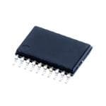
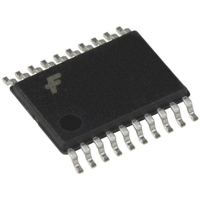
| 产品图片 |
|
| rohs | 符合RoHS无铅 / 符合限制有害物质指令(RoHS)规范要求 |
| 产品系列 | 逻辑集成电路,缓冲器和线路驱动器,Texas Instruments SN74AHC244QPWRG4Q174AHC |
| 数据手册 | |
| 产品型号 | SN74AHC244QPWRG4Q1 |
| 产品种类 | 缓冲器和线路驱动器 |
| 传播延迟时间 | 11.9 ns at 3.3 V |
| 低电平输出电流 | 8 mA |
| 供应商器件封装 | 20-TSSOP |
| 元件数 | 2 |
| 其它名称 | 296-23943-1 |
| 包装 | 剪切带 (CT) |
| 单位重量 | 77 mg |
| 商标 | Texas Instruments |
| 安装类型 | 表面贴装 |
| 安装风格 | SMD/SMT |
| 封装 | Reel |
| 封装/外壳 | 20-TSSOP(0.173",4.40mm 宽) |
| 封装/箱体 | TSSOP-20 |
| 工作温度 | -40°C ~ 125°C |
| 工厂包装数量 | 2000 |
| 最大工作温度 | + 125 C |
| 最小工作温度 | - 40 C |
| 极性 | Non-Inverting |
| 标准包装 | 1 |
| 每元件位数 | 4 |
| 每芯片的通道数量 | 8 |
| 电压-电源 | 2 V ~ 5.5 V |
| 电流-输出高,低 | 8mA,8mA |
| 电源电压-最大 | 5.5 V |
| 电源电压-最小 | 2 V |
| 电源电流 | 0.04 mA |
| 系列 | SN74AHC244-Q1 |
| 输入线路数量 | 8 |
| 输出类型 | 3-State |
| 输出线路数量 | 8 |
| 逻辑类型 | 缓冲器/线路驱动器,非反相 |
| 逻辑系列 | AHC |
| 高电平输出电流 | - 8 mA |


- 商务部:美国ITC正式对集成电路等产品启动337调查
- 曝三星4nm工艺存在良率问题 高通将骁龙8 Gen1或转产台积电
- 太阳诱电将投资9.5亿元在常州建新厂生产MLCC 预计2023年完工
- 英特尔发布欧洲新工厂建设计划 深化IDM 2.0 战略
- 台积电先进制程称霸业界 有大客户加持明年业绩稳了
- 达到5530亿美元!SIA预计今年全球半导体销售额将创下新高
- 英特尔拟将自动驾驶子公司Mobileye上市 估值或超500亿美元
- 三星加码芯片和SET,合并消费电子和移动部门,撤换高东真等 CEO
- 三星电子宣布重大人事变动 还合并消费电子和移动部门
- 海关总署:前11个月进口集成电路产品价值2.52万亿元 增长14.8%


PDF Datasheet 数据手册内容提取
(cid:1)(cid:2)(cid:3)(cid:4)(cid:5)(cid:6)(cid:7)(cid:8)(cid:4)(cid:4)(cid:9)(cid:10)(cid:11) (cid:12)(cid:7)(cid:13)(cid:5)(cid:14) (cid:15)(cid:16)(cid:17)(cid:17)(cid:18)(cid:19)(cid:20)(cid:21)(cid:19)(cid:22)(cid:23)(cid:18)(cid:19) (cid:24)(cid:22)(cid:13)(cid:6) (cid:25)(cid:9)(cid:1)(cid:13)(cid:5)(cid:13)(cid:18) (cid:12)(cid:16)(cid:13)(cid:26)(cid:16)(cid:13)(cid:1) SCLS526A − AUGUST 2003 − REVISED APRIL 2008 (cid:1) Qualified for Automotive Applications DW OR PW PACKAGE (cid:1) (TOP VIEW) ESD Protection Exceeds 1500 V Per MIL-STD-883, Method 3015; Exceeds 150 V Using Machine Model (C = 200 pF, R = 0) 1OE 1 20 VCC 1A1 2 19 2OE (cid:1) EPIC (Enhanced-Performance Implanted 2Y4 3 18 1Y1 CMOS) Process 1A2 4 17 2A4 (cid:1) Operating Range 2-V to 5.5-V VCC 2Y3 5 16 1Y2 1A3 6 15 2A3 description/ordering information 2Y2 7 14 1Y3 1A4 8 13 2A2 This octal buffer/driver is designed specifically to 2Y1 9 12 1Y4 improve the performance and density of 3-state GND 10 11 2A1 memory-address drivers, clock drivers, and bus-oriented receivers and transmitters. The SN74AHC244 is organized as two 4-bit buffers/line drivers with separate output-enable (OE) inputs. When OE is low, the device passes data from the A inputs to the Y outputs. When OE is high, the outputs are in the high-impedance state. To ensure the high-impedance state during power up or power down, OE should be tied to V through a pullup CC resistor; the minimum value of the resistor is determined by the current-sinking capability of the driver. (cid:1) ORDERING INFORMATION ORDERABLE TOP-SIDE TA PACKAGE‡ PART NUMBER MARKING SOIC − DW Tape and reel SN74AHC244QDWRQ1 AHC244Q1 −−4400°°CC ttoo 112255°°CC TSSOP − PW Tape and reel SN74AHC244QPWRQ1 AHC244Q1 †For the most current package and ordering information, see the Package Option Addendum at the end of this document, or see the TI web site at http://www.ti.com. ‡Package drawings, thermal data, and symbolization are available at http://www.ti.com/packaging. FUNCTION TABLE (each 4-bit buffer/driver) INPUTS OOUUTTPPUUTT OE A Y L H H L L L H X Z Please be aware that an important notice concerning availability, standard warranty, and use in critical applications of TexasInstruments semiconductor products and disclaimers thereto appears at the end of this data sheet. EPIC is a trademark of Texas Instruments. (cid:26)(cid:19)(cid:12)(cid:21)(cid:16)(cid:7)(cid:13)(cid:22)(cid:12)(cid:2) (cid:21)(cid:5)(cid:13)(cid:5) (cid:27)(cid:28)(cid:29)(cid:30)(cid:31)!"#(cid:27)(cid:30)(cid:28) (cid:27)$ %&(cid:31)(cid:31)’(cid:28)# "$ (cid:30)(cid:29) (&)*(cid:27)%"#(cid:27)(cid:30)(cid:28) +"#’, Copyright 2008, Texas Instruments Incorporated (cid:26)(cid:31)(cid:30)+&%#$ %(cid:30)(cid:28)(cid:29)(cid:30)(cid:31)! #(cid:30) $(’%(cid:27)(cid:29)(cid:27)%"#(cid:27)(cid:30)(cid:28)$ (’(cid:31) #-’ #’(cid:31)!$ (cid:30)(cid:29) (cid:13)’."$ (cid:22)(cid:28)$#(cid:31)&!’(cid:28)#$ $#"(cid:28)+"(cid:31)+ /"(cid:31)(cid:31)"(cid:28)#0, (cid:26)(cid:31)(cid:30)+&%#(cid:27)(cid:30)(cid:28) ((cid:31)(cid:30)%’$$(cid:27)(cid:28)1 +(cid:30)’$ (cid:28)(cid:30)# (cid:28)’%’$$"(cid:31)(cid:27)*0 (cid:27)(cid:28)%*&+’ #’$#(cid:27)(cid:28)1 (cid:30)(cid:29) "** ("(cid:31)"!’#’(cid:31)$, POST OFFICE BOX 655303 • DALLAS, TEXAS 75265 1
(cid:1)(cid:2)(cid:3)(cid:4)(cid:5)(cid:6)(cid:7)(cid:8)(cid:4)(cid:4)(cid:9)(cid:10)(cid:11) (cid:12)(cid:7)(cid:13)(cid:5)(cid:14) (cid:15)(cid:16)(cid:17)(cid:17)(cid:18)(cid:19)(cid:20)(cid:21)(cid:19)(cid:22)(cid:23)(cid:18)(cid:19) (cid:24)(cid:22)(cid:13)(cid:6) (cid:25)(cid:9)(cid:1)(cid:13)(cid:5)(cid:13)(cid:18) (cid:12)(cid:16)(cid:13)(cid:26)(cid:16)(cid:13)(cid:1) SCLS526A − AUGUST 2003 − REVISED APRIL 2008 logic symbol† 1 19 1OE EN 2OE EN 2 18 11 9 1A1 1Y1 2A1 2Y1 4 16 13 7 1A2 1Y2 2A2 2Y2 6 14 15 5 1A3 1Y3 2A3 2Y3 8 12 17 3 1A4 1Y4 2A4 2Y4 †This symbol is in accordance with ANSI/IEEE Std 91-1984 and IEC Publication 617-12. logic diagram (positive logic) 1 19 1OE 2OE 2 18 11 9 1A1 1Y1 2A1 2Y1 4 16 13 7 1A2 1Y2 2A2 2Y2 6 14 15 5 1A3 1Y3 2A3 2Y3 8 12 17 3 1A4 1Y4 2A4 2Y4 absolute maximum ratings over operating free-air temperature range (unless otherwise noted)† Supply voltage range, V . . . . . . . . . . . . . . . . . . . . . . . . . . . . . . . . . . . . . . . . . . . . . . . . . . . . . . . . . . −0.5 V to 7 V CC Input voltage range, V (see Note 1) . . . . . . . . . . . . . . . . . . . . . . . . . . . . . . . . . . . . . . . . . . . . . . . . . . −0.5 V to 7 V I Output voltage range, VO (see Note 1) . . . . . . . . . . . . . . . . . . . . . . . . . . . . . . . . . . . . . . . . −0.5 V to VCC + 0.5 V Input clamp current, IIK (VI < 0) . . . . . . . . . . . . . . . . . . . . . . . . . . . . . . . . . . . . . . . . . . . . . . . . . . . . . . . . . . . −20 mA Output clamp current, IOK (VO < 0 or VO > VCC) . . . . . . . . . . . . . . . . . . . . . . . . . . . . . . . . . . . . . . . . . . . . ±20 mA Continuous output current, IO (VO = 0 to VCC) . . . . . . . . . . . . . . . . . . . . . . . . . . . . . . . . . . . . . . . . . . . . . . ±25 mA Continuous current through V or GND . . . . . . . . . . . . . . . . . . . . . . . . . . . . . . . . . . . . . . . . . . . . . . . . . . . ±50 mA CC Package thermal impedance, θ (see Note 2): DW package . . . . . . . . . . . . . . . . . . . . . . . . . . . . . . . . . 58°C/W JA PW package . . . . . . . . . . . . . . . . . . . . . . . . . . . . . . . . . 83°C/W Storage temperature range, T . . . . . . . . . . . . . . . . . . . . . . . . . . . . . . . . . . . . . . . . . . . . . . . . . . . −65°C to 150°C stg †Stresses beyond those listed under “absolute maximum ratings” may cause permanent damage to the device. These are stress ratings only, and functional operation of the device at these or any other conditions beyond those indicated under “recommended operating conditions” is not implied. Exposure to absolute-maximum-rated conditions for extended periods may affect device reliability. NOTES: 1. The input and output voltage ratings may be exceeded if the input and output current ratings are observed. 2. The package thermal impedance is calculated in accordance with JESD 51-7. 2 POST OFFICE BOX 655303 • DALLAS, TEXAS 75265
(cid:1)(cid:2)(cid:3)(cid:4)(cid:5)(cid:6)(cid:7)(cid:8)(cid:4)(cid:4)(cid:9)(cid:10)(cid:11) (cid:12)(cid:7)(cid:13)(cid:5)(cid:14) (cid:15)(cid:16)(cid:17)(cid:17)(cid:18)(cid:19)(cid:20)(cid:21)(cid:19)(cid:22)(cid:23)(cid:18)(cid:19) (cid:24)(cid:22)(cid:13)(cid:6) (cid:25)(cid:9)(cid:1)(cid:13)(cid:5)(cid:13)(cid:18) (cid:12)(cid:16)(cid:13)(cid:26)(cid:16)(cid:13)(cid:1) SCLS526A − AUGUST 2003 − REVISED APRIL 2008 recommended operating conditions (see Note 3) MIN MAX UNIT VCC Supply voltage 2 5.5 V VCC = 2 V 1.5 VVIIHH HHiigghh--lleevveell iinnppuutt vvoollttaaggee VCC = 3 V 2.1 VV VCC = 5.5 V 3.85 VCC = 2 V 0.5 VVIILL LLooww--lleevveell iinnppuutt vvoollttaaggee VCC = 3 V 0.9 VV VCC = 5.5 V 1.65 VI Input voltage 0 5.5 V VO Output voltage 0 VCC V VCC = 2 V −50 (cid:1)A IIOOHH HHiigghh--lleevveell oouuttppuutt ccuurrrreenntt VCC = 3.3 V ± 0.3 V −4 mmAA VCC = 5 V ±0.5 V −8 VCC = 2 V 50 (cid:1)A IIOOLL LLooww--lleevveell oouuttppuutt ccuurrrreenntt VCC = 3.3 V ± 0.3 V 4 mmAA VCC = 5 V ±0.5 V 8 VCC = 3.3 V ± 0.3 V 100 ∆∆tt//∆∆vv IInnppuutt ttrraannssiittiioonn rriissee oorr ffaallll rraattee nnss//VV VCC = 5 V ±0.5 V 20 TA Operating free-air temperature −40 125 °C NOTE 3: All unused inputs of the device must be held at VCC or GND to ensure proper device operation. Refer to the TI application report, Implications of Slow or Floating CMOS Inputs, literature number SCBA004. electrical characteristics over recommended operating free-air temperature range (unless otherwise noted) TA = 25°C PPAARRAAMMEETTEERR TTEESSTT CCOONNDDIITTIIOONNSS VVCCCC MMIINN MMAAXX UUNNIITT MIN TYP MAX 2 V 1.9 2 1.9 IIOOHH == −−5500 (cid:1)(cid:1)AA 3 V 2.9 3 2.9 VVOOHH 4.5 V 4.4 4.5 4.4 VV IOH = −4 mA 3 V 2.58 2.48 IOH = −8 mA 4.5 V 3.94 3.8 2 V 0.1 0.1 IIOOLL == 5500 (cid:1)(cid:1)AA 3 V 0.1 0.1 VVOOLL 4.5 V 0.1 0.1 VV IOL = 4 mA 3 V 0.36 0.5 IOL = 8 mA 4.5 V 0.36 0.5 II VI = 5.5 V or GND 0 V to 5.5 V ±0.1 ±1 (cid:1)A IOZ VO = VCC or GND, VI (OE) = VIL or VIH 5.5 V ±0.25 ±2.5 (cid:1)A ICC VI = VCC or GND, IO = 0 5.5 V 4 40 (cid:1)A Ci VI = VCC or GND 5 V 2 10 pF Co VO = VCC or GND 5 V 3.5 pF POST OFFICE BOX 655303 • DALLAS, TEXAS 75265 3
(cid:1)(cid:2)(cid:3)(cid:4)(cid:5)(cid:6)(cid:7)(cid:8)(cid:4)(cid:4)(cid:9)(cid:10)(cid:11) (cid:12)(cid:7)(cid:13)(cid:5)(cid:14) (cid:15)(cid:16)(cid:17)(cid:17)(cid:18)(cid:19)(cid:20)(cid:21)(cid:19)(cid:22)(cid:23)(cid:18)(cid:19) (cid:24)(cid:22)(cid:13)(cid:6) (cid:25)(cid:9)(cid:1)(cid:13)(cid:5)(cid:13)(cid:18) (cid:12)(cid:16)(cid:13)(cid:26)(cid:16)(cid:13)(cid:1) SCLS526A − AUGUST 2003 − REVISED APRIL 2008 switching characteristics over recommended operating free-air temperature range, VCC = 3.3 V±0.3 V (unless otherwise noted) (see Figure 1) FFRROOMM TTOO LLOOAADD TA = 25°C PPAARRAAMMEETTEERR MMIINN MMAAXX UUNNIITT (INPUT) (OUTPUT) CAPACITANCE MIN TYP MAX tPLH 5.8 8.4 1 10 AA YY CCLL == 1155 ppFF nnss tPHL 5.8 8.4 1 10 tPZH 6.6 10.6 1 12.5 OOEE YY CCLL == 1155 ppFF nnss tPZL 6.6 10.6 1 12.5 tPHZ 5 9.7 1 11 OOEE YY CCLL == 1155 ppFF nnss tPLZ 5 9.7 1 11 tPLH 8.3 11.9 1 13.5 AA YY CCLL == 5500 ppFF nnss tPHL 8.3 11.9 1 13.5 tPZH 9.1 14.1 1 16 OOEE YY CCLL == 5500 ppFF nnss tPZL 9.1 14.1 1 16 tPHZ 10.3 14 1 16 OOEE YY CCLL == 5500 ppFF nnss tPLZ 10.3 14 1 16 switching characteristics over recommended operating free-air temperature range, VCC = 5 V±0.5 V (unless otherwise noted) (see Figure 1) FFRROOMM TTOO LLOOAADD TA = 25°C PPAARRAAMMEETTEERR MMIINN MMAAXX UUNNIITT (INPUT) (OUTPUT) CAPACITANCE MIN TYP MAX tPLH 3.9 5.5 1 6.5 AA YY CCLL == 1155 ppFF nnss tPHL 3.9 5.5 1 6.5 tPZH 4.7 7.3 1 8.5 OOEE YY CCLL == 1155 ppFF nnss tPZL 4.7 7.3 1 8.5 tPHZ 5 7.2 1 8.5 OOEE YY CCLL == 1155 ppFF nnss tPLZ 5 7.2 1 8.5 tPLH 5.4 7.5 1 8.5 AA YY CCLL == 5500 ppFF nnss tPHL 5.4 7.5 1 8.5 tPZH 6.2 9.3 1 10.5 OOEE YY CCLL == 5500 ppFF nnss tPZL 6.2 9.3 1 10.5 tPHZ 6.7 9.2 1 10.5 OOEE YY CCLL == 5500 ppFF nnss tPLZ 6.7 9.2 1 10.5 noise characteristics, VCC = 5 V, CL = 50 pF, TA = 25°C (see Note 4) PARAMETER MIN TYP MAX UNIT VOL(P) Quiet output, maximum dynamic VOL 0.5 V VOL(V) Quiet output, minimum dynamic VOL −0.2 V VOH(V) Quiet output, minimum dynamic VOH 4.8 V VIH(D) High-level dynamic input voltage 3.5 V VIL(D) Low-level dynamic input voltage 1.5 V NOTE 4: Characteristics are for surface-mount packages only. 4 POST OFFICE BOX 655303 • DALLAS, TEXAS 75265
(cid:1)(cid:2)(cid:3)(cid:4)(cid:5)(cid:6)(cid:7)(cid:8)(cid:4)(cid:4)(cid:9)(cid:10)(cid:11) (cid:12)(cid:7)(cid:13)(cid:5)(cid:14) (cid:15)(cid:16)(cid:17)(cid:17)(cid:18)(cid:19)(cid:20)(cid:21)(cid:19)(cid:22)(cid:23)(cid:18)(cid:19) (cid:24)(cid:22)(cid:13)(cid:6) (cid:25)(cid:9)(cid:1)(cid:13)(cid:5)(cid:13)(cid:18) (cid:12)(cid:16)(cid:13)(cid:26)(cid:16)(cid:13)(cid:1) SCLS526A − AUGUST 2003 − REVISED APRIL 2008 operating characteristics, VCC = 5 V, TA = 25°C PARAMETER TEST CONDITIONS TYP UNIT Cpd Power dissipation capacitance No load, f = 1 MHz 8.6 pF POST OFFICE BOX 655303 • DALLAS, TEXAS 75265 5
(cid:1)(cid:2)(cid:3)(cid:4)(cid:5)(cid:6)(cid:7)(cid:8)(cid:4)(cid:4)(cid:9)(cid:10)(cid:11) (cid:12)(cid:7)(cid:13)(cid:5)(cid:14) (cid:15)(cid:16)(cid:17)(cid:17)(cid:18)(cid:19)(cid:20)(cid:21)(cid:19)(cid:22)(cid:23)(cid:18)(cid:19) (cid:24)(cid:22)(cid:13)(cid:6) (cid:25)(cid:9)(cid:1)(cid:13)(cid:5)(cid:13)(cid:18) (cid:12)(cid:16)(cid:13)(cid:26)(cid:16)(cid:13)(cid:1) SCLS526A − AUGUST 2003 − REVISED APRIL 2008 PARAMETER MEASUREMENT INFORMATION VCC From Output Test From Output RL = 1 kΩ S1 Open TEST S1 Under Test Point Under Test GND tPLH/tPHL Open CL CL tPLZ/tPZL VCC (see Note A) (see Note A) tPHZ/tPZH GND Open Drain VCC LOAD CIRCUIT FOR LOAD CIRCUIT FOR TOTEM-POLE OUTPUTS 3-STATE AND OPEN-DRAIN OUTPUTS VCC Timing Input 50% VCC tw th 0 V VCC tsu VCC Input 50% VCC 50% VCC Data Input 50% VCC 50% VCC 0 V 0 V VOLTAGE WAVEFORMS VOLTAGE WAVEFORMS PULSE DURATION SETUP AND HOLD TIMES VCC VCC Output Input 50% VCC 50% VCC Control 50% VCC 50% VCC 0 V 0 V tPLH tPHL tPZL tPLZ Output VOH Waveform 1 ≈VCC InO-Puhtapsuet 50% VCC 50% VCC S1 at VCC 50% VCC VOL + 0.3 V VOL (see Note B) VOL tPHL tPLH tPZH tPHZ Output Out-ofO-Puhtapsuet 50% VCC 50% VCVVCOOHL (WseSae1v eNaftoo GtremN B D2) 50% VCC VOH − 0.3 VV≈0O VH VOLTAGE WAVEFORMS VOLTAGE WAVEFORMS PROPAGATION DELAY TIMES ENABLE AND DISABLE TIMES INVERTING AND NONINVERTING OUTPUTS LOW- AND HIGH-LEVEL ENABLING NOTES: A. CL includes probe and jig capacitance. B. Waveform 1 is for an output with internal conditions such that the output is low except when disabled by the output control. Waveform 2 is for an output with internal conditions such that the output is high except when disabled by the output control. C. All input pulses are supplied by generators having the following characteristics: PRR ≤ 1 MHz, ZO = 50 Ω, tr ≤3 ns, tf ≤ 3 ns. D. The outputs are measured one at a time with one input transition per measurement. Figure 1. Load Circuit and Voltage Waveforms 6 POST OFFICE BOX 655303 • DALLAS, TEXAS 75265
PACKAGE OPTION ADDENDUM www.ti.com 11-Apr-2013 PACKAGING INFORMATION Orderable Device Status Package Type Package Pins Package Eco Plan Lead/Ball Finish MSL Peak Temp Op Temp (°C) Top-Side Markings Samples (1) Drawing Qty (2) (3) (4) SN74AHC244QDWRQ1 ACTIVE SOIC DW 20 2000 Green (RoHS CU NIPDAU Level-1-260C-UNLIM -40 to 125 AHC244Q1 & no Sb/Br) SN74AHC244QPWRG4Q1 ACTIVE TSSOP PW 20 2000 Green (RoHS CU NIPDAU Level-1-260C-UNLIM -40 to 125 AHC244Q1 & no Sb/Br) SN74AHC244QPWRQ1 ACTIVE TSSOP PW 20 2000 Green (RoHS CU NIPDAU Level-1-260C-UNLIM -40 to 125 AHC244Q1 & no Sb/Br) (1) The marketing status values are defined as follows: ACTIVE: Product device recommended for new designs. LIFEBUY: TI has announced that the device will be discontinued, and a lifetime-buy period is in effect. NRND: Not recommended for new designs. Device is in production to support existing customers, but TI does not recommend using this part in a new design. PREVIEW: Device has been announced but is not in production. Samples may or may not be available. OBSOLETE: TI has discontinued the production of the device. (2) Eco Plan - The planned eco-friendly classification: Pb-Free (RoHS), Pb-Free (RoHS Exempt), or Green (RoHS & no Sb/Br) - please check http://www.ti.com/productcontent for the latest availability information and additional product content details. TBD: The Pb-Free/Green conversion plan has not been defined. Pb-Free (RoHS): TI's terms "Lead-Free" or "Pb-Free" mean semiconductor products that are compatible with the current RoHS requirements for all 6 substances, including the requirement that lead not exceed 0.1% by weight in homogeneous materials. Where designed to be soldered at high temperatures, TI Pb-Free products are suitable for use in specified lead-free processes. Pb-Free (RoHS Exempt): This component has a RoHS exemption for either 1) lead-based flip-chip solder bumps used between the die and package, or 2) lead-based die adhesive used between the die and leadframe. The component is otherwise considered Pb-Free (RoHS compatible) as defined above. Green (RoHS & no Sb/Br): TI defines "Green" to mean Pb-Free (RoHS compatible), and free of Bromine (Br) and Antimony (Sb) based flame retardants (Br or Sb do not exceed 0.1% by weight in homogeneous material) (3) MSL, Peak Temp. -- The Moisture Sensitivity Level rating according to the JEDEC industry standard classifications, and peak solder temperature. (4) Multiple Top-Side Markings will be inside parentheses. Only one Top-Side Marking contained in parentheses and separated by a "~" will appear on a device. If a line is indented then it is a continuation of the previous line and the two combined represent the entire Top-Side Marking for that device. Important Information and Disclaimer:The information provided on this page represents TI's knowledge and belief as of the date that it is provided. TI bases its knowledge and belief on information provided by third parties, and makes no representation or warranty as to the accuracy of such information. Efforts are underway to better integrate information from third parties. TI has taken and continues to take reasonable steps to provide representative and accurate information but may not have conducted destructive testing or chemical analysis on incoming materials and chemicals. TI and TI suppliers consider certain information to be proprietary, and thus CAS numbers and other limited information may not be available for release. In no event shall TI's liability arising out of such information exceed the total purchase price of the TI part(s) at issue in this document sold by TI to Customer on an annual basis. Addendum-Page 1
PACKAGE OPTION ADDENDUM www.ti.com 11-Apr-2013 OTHER QUALIFIED VERSIONS OF SN74AHC244-Q1 : •Catalog: SN74AHC244 •Enhanced Product: SN74AHC244-EP •Military: SN54AHC244 NOTE: Qualified Version Definitions: •Catalog - TI's standard catalog product •Enhanced Product - Supports Defense, Aerospace and Medical Applications •Military - QML certified for Military and Defense Applications Addendum-Page 2
PACKAGE MATERIALS INFORMATION www.ti.com 20-Dec-2018 TAPE AND REEL INFORMATION *Alldimensionsarenominal Device Package Package Pins SPQ Reel Reel A0 B0 K0 P1 W Pin1 Type Drawing Diameter Width (mm) (mm) (mm) (mm) (mm) Quadrant (mm) W1(mm) SN74AHC244QDWRQ1 SOIC DW 20 2000 330.0 24.4 10.8 13.3 2.7 12.0 24.0 Q1 SN74AHC244QPWRG4Q TSSOP PW 20 2000 330.0 16.4 6.95 7.1 1.6 8.0 16.0 Q1 1 PackMaterials-Page1
PACKAGE MATERIALS INFORMATION www.ti.com 20-Dec-2018 *Alldimensionsarenominal Device PackageType PackageDrawing Pins SPQ Length(mm) Width(mm) Height(mm) SN74AHC244QDWRQ1 SOIC DW 20 2000 367.0 367.0 45.0 SN74AHC244QPWRG4Q1 TSSOP PW 20 2000 367.0 367.0 38.0 PackMaterials-Page2
None
None
PACKAGE OUTLINE DW0020A SOIC - 2.65 mm max height SCALE 1.200 SOIC C 10.63 SEATING PLANE TYP 9.97 A PIN 1 ID 0.1 C AREA 18X 1.27 20 1 13.0 2X 12.6 11.43 NOTE 3 10 11 0.51 20X 7.6 0.31 2.65 MAX B 7.4 0.25 C A B NOTE 4 0.33 TYP 0.10 0.25 SEE DETAIL A GAGE PLANE 0.3 1.27 0 - 8 0.1 0.40 DETAIL A TYPICAL 4220724/A 05/2016 NOTES: 1. All linear dimensions are in millimeters. Dimensions in parenthesis are for reference only. Dimensioning and tolerancing per ASME Y14.5M. 2. This drawing is subject to change without notice. 3. This dimension does not include mold flash, protrusions, or gate burrs. Mold flash, protrusions, or gate burrs shall not exceed 0.15 mm per side. 4. This dimension does not include interlead flash. Interlead flash shall not exceed 0.43 mm per side. 5. Reference JEDEC registration MS-013. www.ti.com
EXAMPLE BOARD LAYOUT DW0020A SOIC - 2.65 mm max height SOIC 20X (2) SYMM 1 20 20X (0.6) 18X (1.27) SYMM (R0.05) TYP 10 11 (9.3) LAND PATTERN EXAMPLE SCALE:6X SOOPLEDNEINRG MASK METAL MSOELTDAEL RU NMDAESRK SOOPLEDNEINRG MASK 0.07 MAX 0.07 MIN ALL AROUND ALL AROUND NON SOLDER MASK SOLDER MASK DEFINED DEFINED SOLDER MASK DETAILS 4220724/A 05/2016 NOTES: (continued) 6. Publication IPC-7351 may have alternate designs. 7. Solder mask tolerances between and around signal pads can vary based on board fabrication site. www.ti.com
EXAMPLE STENCIL DESIGN DW0020A SOIC - 2.65 mm max height SOIC 20X (2) SYMM 1 20 20X (0.6) 18X (1.27) SYMM 10 11 (9.3) SOLDER PASTE EXAMPLE BASED ON 0.125 mm THICK STENCIL SCALE:6X 4220724/A 05/2016 NOTES: (continued) 8. Laser cutting apertures with trapezoidal walls and rounded corners may offer better paste release. IPC-7525 may have alternate design recommendations. 9. Board assembly site may have different recommendations for stencil design. www.ti.com
IMPORTANTNOTICEANDDISCLAIMER TIPROVIDESTECHNICALANDRELIABILITYDATA(INCLUDINGDATASHEETS),DESIGNRESOURCES(INCLUDINGREFERENCE DESIGNS),APPLICATIONOROTHERDESIGNADVICE,WEBTOOLS,SAFETYINFORMATION,ANDOTHERRESOURCES“ASIS” ANDWITHALLFAULTS,ANDDISCLAIMSALLWARRANTIES,EXPRESSANDIMPLIED,INCLUDINGWITHOUTLIMITATIONANY IMPLIEDWARRANTIESOFMERCHANTABILITY,FITNESSFORAPARTICULARPURPOSEORNON-INFRINGEMENTOFTHIRD PARTYINTELLECTUALPROPERTYRIGHTS. TheseresourcesareintendedforskilleddevelopersdesigningwithTIproducts.Youaresolelyresponsiblefor(1)selectingtheappropriate TIproductsforyourapplication,(2)designing,validatingandtestingyourapplication,and(3)ensuringyourapplicationmeetsapplicable standards,andanyothersafety,security,orotherrequirements.Theseresourcesaresubjecttochangewithoutnotice.TIgrantsyou permissiontousetheseresourcesonlyfordevelopmentofanapplicationthatusestheTIproductsdescribedintheresource.Other reproductionanddisplayoftheseresourcesisprohibited.NolicenseisgrantedtoanyotherTIintellectualpropertyrightortoanythird partyintellectualpropertyright.TIdisclaimsresponsibilityfor,andyouwillfullyindemnifyTIanditsrepresentativesagainst,anyclaims, damages,costs,losses,andliabilitiesarisingoutofyouruseoftheseresources. TI’sproductsareprovidedsubjecttoTI’sTermsofSale(www.ti.com/legal/termsofsale.html)orotherapplicabletermsavailableeitheron ti.comorprovidedinconjunctionwithsuchTIproducts.TI’sprovisionoftheseresourcesdoesnotexpandorotherwisealterTI’sapplicable warrantiesorwarrantydisclaimersforTIproducts. MailingAddress:TexasInstruments,PostOfficeBox655303,Dallas,Texas75265 Copyright©2018,TexasInstrumentsIncorporated