
 Datasheet下载
- 型号: SMA6T47AY
- 制造商: STMicroelectronics
- 库位|库存: xxxx|xxxx
- 要求:
| 数量阶梯 | 香港交货 | 国内含税 |
| +xxxx | $xxxx | ¥xxxx |
查看当月历史价格
查看今年历史价格
SMA6T47AY产品简介:
ICGOO电子元器件商城为您提供SMA6T47AY由STMicroelectronics设计生产,在icgoo商城现货销售,并且可以通过原厂、代理商等渠道进行代购。 SMA6T47AY价格参考¥1.01-¥1.01。STMicroelectronicsSMA6T47AY封装/规格:TVS - 二极管, 。您可以下载SMA6T47AY参考资料、Datasheet数据手册功能说明书,资料中有SMA6T47AY 详细功能的应用电路图电压和使用方法及教程。
STMicroelectronics的SMA6T47AY是一款TVS(瞬态电压抑制)二极管,主要应用于电路保护领域。其应用场景如下:

1. 过压保护:SMA6T47AY能够有效抑制电路中的瞬态过电压,如雷击、电感负载开关和静电放电等引起的电压浪涌,从而保护敏感电子元件。

2. 通信接口保护:适用于RS-232、RS-485、USB等通信接口,防止外部干扰或电压浪涌对数据传输的影响。

3. 电源线保护:在电源输入端使用,可防止因电网波动或负载切换引起的电压尖峰损坏设备。

4. 汽车电子保护:可用于汽车电子系统中,如车载充电器、传感器和控制模块,抵御由点火系统或 alternator 产生的瞬态电压。

5. 工业自动化设备:为工业控制系统中的信号线和电源线提供保护,确保设备稳定运行。

6. 消费电子产品:用于家用电器、音频/视频设备等,防止因插拔或外部环境因素导致的电压异常。

SMA6T47AY具有低电容、快速响应时间和高浪涌电流能力,适合多种需要可靠保护的应用场合。
| 参数 | 数值 |
| 产品目录 | |
| 描述 | TVS DIODE 40VWM 73.6VC SMA |
| 产品分类 | |
| 品牌 | STMicroelectronics |
| 数据手册 | |
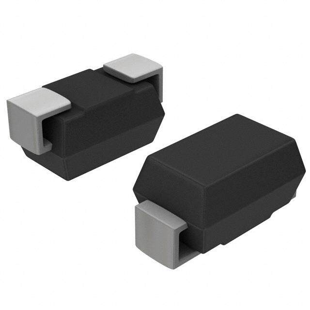
| 产品图片 |
|
| 产品型号 | SMA6T47AY |
| rohs | 无铅 / 符合限制有害物质指令(RoHS)规范要求 |
| 产品系列 | SMA6T, TRANSIL™ |
| 不同频率时的电容 | - |
| 产品培训模块 | http://www.digikey.cn/PTM/IndividualPTM.page?site=cn&lang=zhs&ptm=26067 |
| 供应商器件封装 | SMA (DO-214AC) |
| 其它名称 | 497-11829-6 |
| 其它有关文件 | http://www.st.com/web/catalog/sense_power/FM114/CL1801/SC1495/PF251009?referrer=70071840 |
| 功率-峰值脉冲 | 600W |
| 包装 | Digi-Reel® |
| 单向通道 | 1 |
| 双向通道 | - |
| 安装类型 | 表面贴装 |
| 封装/外壳 | DO-214AC,SMA |
| 工作温度 | -40°C ~ 150°C (TJ) |
| 应用 | 自动 |
| 标准包装 | 1 |
| 电压-击穿(最小值) | 44.4V |
| 电压-反向关态(典型值) | 40V |
| 电压-箝位(最大值)@Ipp | 73.6V |
| 电流-峰值脉冲(10/1000µs) | 48A (8/20µs) |
| 电源线路保护 | 无 |
| 类型 | 齐纳 |


- 商务部:美国ITC正式对集成电路等产品启动337调查
- 曝三星4nm工艺存在良率问题 高通将骁龙8 Gen1或转产台积电
- 太阳诱电将投资9.5亿元在常州建新厂生产MLCC 预计2023年完工
- 英特尔发布欧洲新工厂建设计划 深化IDM 2.0 战略
- 台积电先进制程称霸业界 有大客户加持明年业绩稳了
- 达到5530亿美元!SIA预计今年全球半导体销售额将创下新高
- 英特尔拟将自动驾驶子公司Mobileye上市 估值或超500亿美元
- 三星加码芯片和SET,合并消费电子和移动部门,撤换高东真等 CEO
- 三星电子宣布重大人事变动 还合并消费电子和移动部门
- 海关总署:前11个月进口集成电路产品价值2.52万亿元 增长14.8%


PDF Datasheet 数据手册内容提取
SMA6TY Datasheet Automotive 600 W TVS in SMA Features • AEC-Q101 qualified • Peak pulse power: – 600 W (10/1000 μs) and 4 kW (8/20 μs) • Stand-off voltage range: from 5 V to 70 V • Unidirectional and bidirectional types • Low leakage current: – 0.2 μA at 25 °C and 1 μA at 85 °C • Operating T max: 150 °C j • JEDEC registered package outline • Lead finishing: matte tin plating Complies with the following standards • UL94, V0 • J-STD-020 MSL level 1 • J-STD-002, JESD 22-B102 E3 and MIL-STD-750, method 2026 • JESD-201 class 2 whisker test • IPC7531 footprint and JEDEC registered package outline • IEC 61000-4-4 level 4 Product status link – 4 k V • ISO 10605, IEC 61000-4-2, C = 150 pF, R = 330 Ω exceeds level 4: SMA6TY – 30 kV (air discharge) – 30 kV (contact discharge) • ISO 10605, C = 330 pF, R = 330 Ω exceeds level 4: – 30 kV (air discharge) – 30 kV (contact discharge) • ISO 7637-2 (not applicable to parts with V lower than battery voltage) RM – Pulse 1: V = -150 V S – Pulse 2a: V = +112 V S – Pulse 3a: V = -220 V S – Pulse3b: V = +150 V S Description The SMA6TY Transil series has been designed to protect sensitive automotive circuits against surges defined in ISO 7637-2 and against electrostatic discharges according to ISO 10605. The planar technology makes this device compatible with high-end circuits where low leakage current and high junction temperature are required to provide reliability and stability over time. SMA6TY are packaged in SMA. Transil™ is a trademark of STMicroelectronics. DS6931 - Rev 5 - December 2018 www.st.com For further information contact your local STMicroelectronics sales office.
SMA6TY Characteristics 1 Characteristics Table 1. Absolute maximum ratings (T = 25 °C) amb Symbol Parameter Value Unit ISO10605 (C = 330 pF, R = 330 Ω): Contact discharge 30 Air discharge 30 VPP Peak pulse voltage kV ISO10605 / IEC 61000-4-2 (C = 150 pF, R = 330 Ω) 30 Contact discharge 30 Air discharge PPP Peak pulse power dissipation 10/1000 µs, Tj initial = Tamb 600 W Tj Operating junction temperature range -40 to +150 °C Tstg Storage temperature range -65 to +150 °C TL Maximum lead temperature for soldering during 10 s 260 °C Figure 1. Electrical characteristics - parameter definitions Bidirectional device Unidirectional device I I VRM Stand-off voltage IPP PP I Leakage current @ V RM RM V Breakdown voltage BR I IVVPCFPL CFPoelaramwk papriundlg sv evo ocltulatragrgeee nd trop VCLVBR VRM IRIRM IRIM VRMVBR VCVL V VF IRRM VRMVBRVCL αT Voltage temperature coefficient R R Dynamic resistance I I D IPP V IF V I DS6931 - Rev 5 page 2/13
SMA6TY Characteristics Table 2. Electrical characteristics (T = 25 °C, unless otherwise specified) amb IRM max at VRM VBR at IR 10 / 1000 µs 8 / 20µs αT(1) VCL(2) IPP(3) RD VCL(2) IPP(3) RD Order code 25 °C 85 °C Min. Typ. Max. Max. Max. Max. Max. µA V V mA V A Ω V A Ω 10-4/°C SMA6T6V7AY/CAY 20 50 5.00 6.40 6.40 7.1 10 9.1 68.0 0.029 14.4 275 0.027 5.7 SMA6T7V6AY/CAY 20 50 6.50 7.20 7.60 8.0 10 10.2 56.0 0.04 15.2 266 0.027 6.1 SMA6T10AY/CAY 20 50 8.60 9.50 10.0 10.5 1 14.5 41.0 0.098 18.6 215 0.038 7.3 SMA6T12AY/CAY 0.2 1 10.2 11.4 12.0 12.6 1 16.7 36.0 0.114 21.7 184 0.049 7.8 SMA6T14AY/CAY 0.2 1 12.0 13.3 14.0 14.7 1 18.8 31.0 0.133 23.5 157 0.056 8.3 SMA6T15AY/CAY 0.2 1 12.8 14.3 15.0 15.8 1 21.2 28.0 0.193 27.2 147 0.078 8.4 SMA6T18AY/CAY 0.2 1 15.3 17.1 18.0 18.9 1 25.2 24.0 0.263 32.3 123 0.111 8.8 SMA6T22AY/CAY 0.2 1 18.8 20.9 22.0 23.1 1 30.6 20.0 0.375 39.3 102 0.159 9.2 SMA6T24AY/CAY 0.2 1 20.5 22.8 24.0 25.2 1 33.2 18.0 0.444 42.8 93.0 0.189 9.4 SMA6T28AY/CAY 0.2 1 24 26.7 28.1 29.5 1 37.8 16.0 0.516 44.3 80.0 0.184 9.6 SMA6T30AY/CAY 0.2 1 25.6 28.5 30.0 31.5 1 41.5 14.5 0.690 53.5 75.0 0.293 9.7 SMA6T33AY/CAY 0.2 1 28.2 31.4 33.0 34.7 1 45.7 13.1 0.840 59.0 68.0 0.357 9.8 SMA6T39AY/CAY 0.2 1 33.3 37.1 39.0 41.0 1 53.9 11.1 1.16 69.7 57.0 0.504 10.0 SMA6T47AY/CAY 0.2 1 40.0 44.4 46.7 49.1 1 62.8 9.70 1.42 73.6 48.0 0.511 10.1 SMA6T56AY/CAY 0.2 1 47.6 53.2 56.0 58.8 1 76.6 7.80 2.28 100 40 1.030 10.0 SMA6T68AY/CAY 0.2 1 58.1 64.6 68.0 71.4 1 92.0 6.50 3.17 121 33.0 1.50 10.4 SMA6T82AY/CAY 0.2 1 70.0 77.8 81.9 86.0 1 110 5.50 4.38 120 27 1.030 10.5 1. To calculate VBR or VCL versus junction temperature, use the following formulas: • VBR at TJ = VBR at 25 °C x (1 + αT x (TJ - 25)) • VCL at TJ = VCL at 25 °C x (1 + αT x (TJ-25)) 2. To calculate maximum clamping voltage at other surge level, use the following formula: • VCLmax = VBR max + RD x IPPappli where IPPappli is the surge current in the application 3. Surge capability given for both directions for unidirectional and bidirectional types. DS6931 - Rev 5 page 3/13
SMA6TY Characteristics (curves) 1.1 Characteristics (curves) Figure 3. Relative variation of peak power versus initial Figure 2. Pulse definition for electrical characteristics junction temperature 110 IPP% 110 % 100 tr 100 10/1000 µs 90 tr = risetime tp = pulse duration time 90 80 80 70 70 60 60 tp 50 50 40 40 30 30 20 20 10 t (µs) 10 T(°C) j 0 0 0 25 50 75 100 125 150 175 Figure 4. Maximum peak pulse power versus exponential Figure 5. Maximum clamping voltage versus peak pulse pulse duration current exponential waveform (maximum values) PPP(kW) IPP(A) 10.0 1000.0 Tjinitial = 25°C Tjinitial=25°C 100.0 8/20 µs 1.0 10.0 10/1000 µs tP(ms) 1.0 SMA6T6V7AY/CAY SMA6T30AY/CAY SMA6T82AY/CAY VVCCLL((VV)) 0.1 0.1 0.01 0.10 1.00 10.00 1 10 100 1000 DS6931 - Rev 5 page 4/13
SMA6TY Characteristics (curves) Figure 6. Junction capacitance versus reverse applied Figure 7. Junction capacitance versus reverse applied voltage for unidirectional types voltage for bidirectional types C(pF) C(pF) 10000 10000 F=1 MHz F=1 MHz VOSC=30 mVRMS VOSC=30 mVRMS Tj=25°C Tj=25°C SMA6T6V7AY 1000 1000 SMA6T6V7CAY SMA6T30AY 100 100 SMA6T30CAY SMA6T82AY SMA6T82CAY VR(V) 10 VR(V) 10 1 10 100 1000 1 10 100 1000 Figure 9. Peak forward voltage drop versus peak forward Figure 8. Leakage current versus junction temperature current 1.E+04 IR(nA) IFM(A) VR=VRM 1.E+01 1.E+03 VRM≤10V Tj=125°C 1.E+00 1.E+02 Tj=25°C 1.E+01 VRM>10V 1.E-01 T(°C) j 1.E+00 VFM(V) 25 50 75 100 125 150 1.E-02 0.4 0.5 0.6 0.7 0.8 0.9 1.0 1.1 1.2 1.3 1.4 Figure 10. Relative variation of thermal impedance, junction to ambient, versus pulse duration Figure 11. Thermal resistance junction to ambient versus copper surface under each lead Zth (j-a)/Rth (j-a) 1.00 Rth(j-a) (°C/W) 200 Printed circuit board FR4, Single pulse on recommended footprint.Epoxy printed circuit copper surface = 1 cm2 board FR4, 70µm Cu thickness 150 0.10 100 50 tp s 0.01 SCu (cm²) 1.E-02 1.E-01 1.E+00 1.E+01 1.E+02 1.E+03 00 0.5 1 1.5 2 2.5 3 3.5 4 4.5 5 DS6931 - Rev 5 page 5/13
SMA6TY Characteristics (curves) Figure 12. ISO7637-2 pulse 1: Vs = -150 V with 12 V Figure 13. ISO7637-2 pulse 2a: Vs = +112 V with 12 V battery battery 10 V/div 10 V/div SMA6T30AY SMA6T30CAY SMA6T30AY SMA6T30CAY 10 A /div 10 µs /div 5 A /div 500 µs /div Figure 14. ISO7637-2 pulse 3a: Vs = -220 V with 12 V Figure 15. ISO7637-2 pulse 3b: Vs = +150 V with 12 V battery battery 10 V/div 10 V/div SMA6T30AY SMA6T30AY SMA6T30CAY SMA6T30CAY 1 A /div 200 ns /div 1 A /div 200 ns /div DS6931 - Rev 5 page 6/13
SMA6TY Package information 2 Package information In order to meet environmental requirements, ST offers these devices in different grades of ECOPACK® packages, depending on their level of environmental compliance. ECOPACK® specifications, grade definitions and product status are available at: www.st.com. ECOPACK® is an ST trademark. 2.1 SMA package information Figure 16. SMA package outline E1 D E A1 C A2 L b Table 3. SMA package mechanical data Dimensions Ref. Millimeters Inches Min. Max. Min. Max. A1 1.90 2.45 0.074 0.097 A2 0.05 0.20 0.001 0.008 b 1.25 1.65 0.049 0.065 c 0.15 0.40 0.005 0.016 D 2.25 2.90 0.088 0.115 E 4.80 5.35 0.188 0.211 E1 3.95 4.60 0.155 0.182 L 0.75 1.50 0.029 0.060 DS6931 - Rev 5 page 7/13
SMA6TY SMA package information Figure 17. SMA recommended footprint in mm (inches) Figure 18. SMA marking 1.40 2.63 1.40 (0.055) (0.104) (0.055) 1.64 (0.065) 5.43 (0.214) Figure 19. Package orientation in reel Figure 20. Tape and reel orientation Figure 21. 13'' reel dimension values Figure 22. Inner box dimension values DS6931 - Rev 5 page 8/13
SMA6TY SMA package information Figure 23. Tape outline Table 4. Tape dimension values Dimensions Ref. Millimeters Min. Typ. Max. D0 1.40 1.50 1.60 D1 1.50 F 5.40 5.50 5.60 K0 2.26 2.36 2.46 P0 3.90 4.00 4.10 P1 3.90 4.00 4.10 P2 1.95 2.00 2.05 W 11.70 12.00 12.30 DS6931 - Rev 5 page 9/13
SMA6TY Ordering information 3 Ordering information Figure 24. Ordering information scheme SMA 6T X X CA Y Surface mount SMA = SMA package Peak pulse power 6 = 60 0 W Transil Breakdown voltage 30 = 30 V Types CA = Bidirectional A = Unidirectional Automotive grade Table 5. Ordering information Order code Marking Package Weight Base qty. Delivery mode SMA6TxxxAY/CAYSection 3 See Table 6. Marking. SMA 0.072 g 5000 Tape and reel DS6931 - Rev 5 page 10/13
SMA6TY Ordering information Table 6. Marking Order code Marking Order code Marking SMA6T6V7AY 6UAY SMA6T6V7CAY 6BAY SMA6T7V6AY 6UCY SMA6T7V6CAY 6BCY SMA6T10AY 6UDY SMA6T10CAY 6BDY SMA6T12AY 6UEY SMA6T12CAY 6BEY SMA6T14AY 6UFY SMA6T14CAY 6BFY SMA6T15AY 6UGY SMA6T15CAY 6BGY SMA6T18AY 6UHY SMA6T18CAY 6BHY SMA6T22AY 6UJY SMA6T22CAY 6BJY SMA6T24AY 6UKY SMA6T24CAY 6BKY SMA6T28AY 6UMY SMA6T28CAY 6BMY SMA6T30AY 6UNY SMA6T30CAY 6BNY SMA6T33AY 6UOY SMA6T33CAY 6BOY SMA6T39AY 6UQY SMA6T39CAY 6BQY SMA6T47AY 6URY SMA6T47CAY 6BRY SMA6T56AY 6USY SMA6T56CAY 6BSY SMA6T68AY 6UTY SMA6T68CAY 6BTY SMA6T82AY 6UUY SMA6T82CAY 6BUY DS6931 - Rev 5 page 11/13
SMA6TY Revision history Table 7. Document revision history Date Revision Changes 15-Sep-2010 1 Initial release. Deleted old Table 2. Thermal parameter. Updated Table 2 and added order codes in Table 4. 18-Oct-2011 2 Updated Figure 5, Figure 10 and Figure 11. 27-Mar-2012 3 Added footnote on page 1. 25-Jan-2018 4 Updated Table 2. Electrical characteristics (Tamb = 25 °C, unless otherwise specified). 07-Dec-2018 5 Updated Table 5. Ordering information. DS6931 - Rev 5 page 12/13
SMA6TY IMPORTANT NOTICE – PLEASE READ CAREFULLY STMicroelectronics NV and its subsidiaries (“ST”) reserve the right to make changes, corrections, enhancements, modifications, and improvements to ST products and/or to this document at any time without notice. Purchasers should obtain the latest relevant information on ST products before placing orders. ST products are sold pursuant to ST’s terms and conditions of sale in place at the time of order acknowledgement. Purchasers are solely responsible for the choice, selection, and use of ST products and ST assumes no liability for application assistance or the design of Purchasers’ products. No license, express or implied, to any intellectual property right is granted by ST herein. Resale of ST products with provisions different from the information set forth herein shall void any warranty granted by ST for such product. ST and the ST logo are trademarks of ST. All other product or service names are the property of their respective owners. Information in this document supersedes and replaces information previously supplied in any prior versions of this document. © 2018 STMicroelectronics – All rights reserved DS6931 - Rev 5 page 13/13