
 Datasheet下载
- 型号: SMA6F13A-M3/6A
- 制造商: Vishay
- 库位|库存: xxxx|xxxx
- 要求:
| 数量阶梯 | 香港交货 | 国内含税 |
| +xxxx | $xxxx | ¥xxxx |
查看当月历史价格
查看今年历史价格
SMA6F13A-M3/6A产品简介:
ICGOO电子元器件商城为您提供SMA6F13A-M3/6A由Vishay设计生产,在icgoo商城现货销售,并且可以通过原厂、代理商等渠道进行代购。 SMA6F13A-M3/6A价格参考。VishaySMA6F13A-M3/6A封装/规格:TVS - 二极管, 。您可以下载SMA6F13A-M3/6A参考资料、Datasheet数据手册功能说明书,资料中有SMA6F13A-M3/6A 详细功能的应用电路图电压和使用方法及教程。
Vishay Semiconductor Diodes Division的SMA6F13A-M3/6A是一款表面贴装TVS(瞬态电压抑制)二极管,主要用于保护电子电路免受静电放电(ESD)、浪涌和其它瞬态电压的损害。该器件具有快速响应时间和高浪涌吸收能力,适用于对敏感电子元件进行高效保护。

典型应用场景包括:

1. 通信设备:用于保护以太网端口、USB接口、RS-485等通信线路,防止因雷击或静电引起的电压突变损坏主芯片。
2. 工业控制系统:在PLC、传感器接口和自动化设备中提供瞬态电压保护,提升系统稳定性和可靠性。
3. 消费电子产品:如智能手机、平板电脑和可穿戴设备中的数据线与充电接口保护。
4. 汽车电子:用于车载娱乐系统、控制模块和CAN总线接口的瞬态电压防护。
5. 电源管理电路:在DC电源输入端作为第一道防线,吸收来自外部环境的高压脉冲。

综上,SMA6F13A-M3/6A适用于需要高水平瞬态电压保护的各种电子系统,特别适合空间有限且要求高性能的表面贴装应用。
| 参数 | 数值 |
| 产品目录 | |
| 描述 | TVS DIODE 13VWM 23.9VC DO221ACTVS 二极管 - 瞬态电压抑制器 600W 13V 5% Uni Low Profile |
| 产品分类 | |
| 品牌 | Vishay SemiconductorsVishay Semiconductor Diodes Division |
| 产品手册 | |
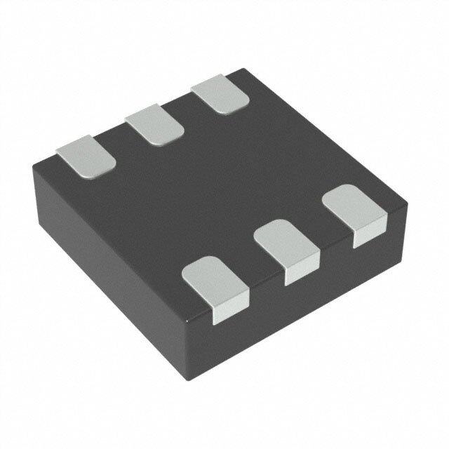
| 产品图片 |
|
| rohs | 符合RoHS无铅 / 符合限制有害物质指令(RoHS)规范要求 |
| 产品系列 | 二极管与整流器,TVS二极管,TVS 二极管 - 瞬态电压抑制器,Vishay Semiconductors SMA6F13A-M3/6ATransZorb® |
| 数据手册 | |
| 产品型号 | SMA6F13A-M3/6ASMA6F13A-M3/6A |
| 不同频率时的电容 | - |
| 产品种类 | TVS 二极管 - 瞬态电压抑制器 |
| 供应商器件封装 | DO-221AC |
| 其它名称 | SMA6F13A-M3/6AGIDKR |
| 击穿电压 | 15.9 V |
| 功率-峰值脉冲 | 4000W (4kW) |
| 包装 | Digi-Reel® |
| 单向通道 | 1 |
| 双向通道 | - |
| 商标 | Vishay Semiconductors |
| 商标名 | TransZorb |
| 安装类型 | 表面贴装 |
| 安装风格 | SMD/SMT |
| 封装 | Reel |
| 封装/外壳 | DO-221AC,SMA 扁平引线 |
| 封装/箱体 | DO-221AC |
| 尺寸 | 2.7 mm W x 5.35 mm L x 1 mm H |
| 峰值浪涌电流 | 29.4 A |
| 峰值脉冲功率耗散 | 600 W |
| 工作温度 | -55°C ~ 175°C (TJ) |
| 工作电压 | 13 V |
| 应用 | 通用 |
| 最大工作温度 | + 125 C |
| 最小工作温度 | - 55 C |
| 极性 | Unidirectional |
| 标准包装 | 1 |
| 特色产品 | http://www.digikey.com/product-highlights/cn/zh/vishay-sma6f-voltage-suppressors/2051 |
| 电压-击穿(最小值) | 14.4V |
| 电压-反向关态(典型值) | 13V |
| 电压-箝位(最大值)@Ipp | 23.9V |
| 电流-峰值脉冲(10/1000µs) | 147A (8/20µs) |
| 电源线路保护 | 无 |
| 端接类型 | SMD/SMT |
| 类型 | 齐纳 |
| 系列 | SMA6F |
| 钳位电压 | 20.4 V |


- 商务部:美国ITC正式对集成电路等产品启动337调查
- 曝三星4nm工艺存在良率问题 高通将骁龙8 Gen1或转产台积电
- 太阳诱电将投资9.5亿元在常州建新厂生产MLCC 预计2023年完工
- 英特尔发布欧洲新工厂建设计划 深化IDM 2.0 战略
- 台积电先进制程称霸业界 有大客户加持明年业绩稳了
- 达到5530亿美元!SIA预计今年全球半导体销售额将创下新高
- 英特尔拟将自动驾驶子公司Mobileye上市 估值或超500亿美元
- 三星加码芯片和SET,合并消费电子和移动部门,撤换高东真等 CEO
- 三星电子宣布重大人事变动 还合并消费电子和移动部门
- 海关总署:前11个月进口集成电路产品价值2.52万亿元 增长14.8%


PDF Datasheet 数据手册内容提取
SMA6F5.0A thru SMA6F20A www.vishay.com Vishay General Semiconductor Surface-Mount TRANSZORB® Transient Voltage Suppressors FEATURES eSMP® Series • Very low profile - typical height of 0.95 mm • Ideal for automated placement • Uni-directional only • Excellent clamping capability • Peak pulse power: Top View Bottom View - 600 W (10/1000 μs) - 4 kW (8/20 μs) SlimSMA (DO-221AC) • ESD capability: IEC 61000-4-2 level 4 - 15 kV (air) Cathode Anode - 8 kV (contact) • Meets MSL level 1, per J-STD-020, LF maximum peak of 260 °C DESIGN SUPPORT TOOLS click logo to get started • Material categorization: for definitions of compliance please see www.vishay.com/doc?99912 Models Available TYPICAL APPLICATIONS Use in sensitive electronics protection against voltage transients induced by inductive load switching and lighting PRIMARY CHARACTERISTICS on ICs, MOSFET, signal lines of sensor units for consumer, computer, industrial, and telecommunication. V 6.4 V to 24.5 V BR V 5.0 V to 20 V MECHANICAL DATA WM PPPM (10 x 1000 μs) 600 W Case: SlimSMA (DO-221AC) P (8 x 20 μs) 4000 W Molding compound meets UL 94 V-0 flammability rating PPM Base P/N-M3 - halogen-free, RoHS-compliant, and P at T = 55 °C 6 W D M industrial grade T max. 175 °C J Terminals: matte tin plated leads, solderable per Polarity Uni-directional J-STD-002 and JESD22-B102 Package SlimSMA (DO-221AC) M3 suffix meets JESD 201 class 2 whisker test Polarity: color band denotes cathode end MAXIMUM RATINGS (T = 25 °C, unless otherwise noted) A PARAMETER SYMBOL VALUE UNIT with a 10/1000 μs waveform 600 Peak pulse power dissipation P (1) W PPM with a 8/20 μs waveform 4000 with a 10/1000 μs waveform Peak pulse current I (1) See next table A PPM with a 8/20 μs waveform T = 55 °C P (2) 6 M D Power dissipation W T = 25 °C P (3) 1.0 A D Storage temperature range T -65 to +175 STG °C Operating junction temperature range T -55 to +175 J Notes (1) Non-repetitive current pulse, per fig. 3 and derated above T = 25 °C per fig. 2. A (2) Power dissipation mounted on infinite heatsink (3) Power dissipation mounted on minimum recommended pad layout Revision: 16-Oct-2018 1 Document Number: 89458 For technical questions within your region: DiodesAmericas@vishay.com, DiodesAsia@vishay.com, DiodesEurope@vishay.com THIS DOCUMENT IS SUBJECT TO CHANGE WITHOUT NOTICE. THE PRODUCTS DESCRIBED HEREIN AND THIS DOCUMENT ARE SUBJECT TO SPECIFIC DISCLAIMERS, SET FORTH AT www.vishay.com/doc?91000
SMA6F5.0A thru SMA6F20A www.vishay.com Vishay General Semiconductor INDEX OF SYMBOLS SYMBOL PARAMETER IF V Stand-off voltage WM VBR Breakdown voltage VWM V V Clamping voltage BR C V C ID Leakage current at VWM VF V I I Peak pulse current D PP I T T Voltage temperature coefficient V Forward voltage drop F RD Dynamic resistance IPP Zener Voltage Regulator ELECTRICAL CHARACTERISTICS (T = 25 °C unless otherwise noted) A STAND MAXIMUM V AT I R (2) V AT I R (2) BREAKDOWN C PP D C PP D -OFF REVERSE VOLTAGE T (3) DTYEPVEICE MDAERVKICINEG VBR AT IT (1) VOVLWTAMG E IDL EAAT KVAWGME (3) 10/1000 μs 8/20 μs CODE MIN. MAX. 25 °C 85 °C MAX. MAX. MAX. V mA V μA V V A V A 10-4/°C SMA6F5.0A 6AE 6.40 7.07 10 5 150 375 5.0 9.2 68.0 0.031 13.4 298 0.021 5.7 SMA6F6.0A 6AG 6.70 7.41 10 6 600 1500 6.0 9.5 63.2 0.033 13.7 290 0.022 5.9 SMA6F6.5A 6AK 7.20 7.96 10 6.5 100 250 6.5 10.2 58.8 0.038 14.5 276 0.024 6.1 SMA6F7.5A 6AP 8.33 9.21 1 7.5 50 125 7.5 11.8 50.8 0.051 17.0 235 0.033 6.5 SMA6F8.0A 6AR 8.89 9.83 1 8.0 20 50 8.0 12.8 46.9 0.063 18.2 220 0.038 7.0 SMA6F8.5A 6AT 9.4 10.4 1 8.5 20 50 8.5 13.3 45.1 0.064 18.7 205 0.040 7.3 SMA6F10A 6AX 11.1 12.3 1 10 1.0 5.0 10 15.7 38.2 0.089 19.6 184 0.040 7.8 SMA6F11A 6AZ 12.2 13.5 1 11 1.0 5.0 11 17.2 34.8 0.107 21.5 172 0.047 8.1 SMA6F12A 6BE 13.3 14.7 1 12 0.2 1.0 12 18.8 31.9 0.128 23.5 157 0.056 8.3 SMA6F12AHD 6BF 13.2 14.3 1 12 0.2 1.0 12 18.5 32.4 0.130 22.9 157 0.055 8.4 SMA6F13A 6BG 14.4 15.9 1 13 0.2 1.0 13 20.4 29.4 0.153 23.9 147 0.064 8.4 SMA6F15A 6BM 16.7 18.5 1 15 0.2 1.0 15 23.6 25.4 0.201 27.7 123 0.075 8.8 SMA6F16A 6BP 17.8 19.7 1 16 0.2 1.0 16 25.2 23.8 0.229 29.5 119 0.082 8.8 SMA6F17A 6BR 18.9 20.9 1 17 0.2 1.0 17 26.7 22.5 0.259 31.4 111 0.095 9.0 SMA6F18A 6BT 20.0 22.1 1 18 0.2 1.0 18 28.3 21.2 0.292 33.2 102 0.109 9.2 SMA6F20A 6BV 22.2 24.5 1 20 0.2 1.0 20 31.4 19.1 0.361 36.8 93 0.132 9.4 Notes (1) Pulse test: tp 50 ms (2) To calculate maximum clamping voltage at other surge currents, use following formula: V max. = R x I + V max. CL D PP BR (3) To calculate VBR vs. junction temperature, use following formula: VBR at TJ = VBR at 25 °C x (1 + T x (TJ - 25)) THERMAL CHARACTERISTICS (T = 25 °C unless otherwise noted) A PARAMETER SYMBOL VALUE UNIT Typical thermal resistance, junction to ambient R (1) 150 JA °C/W Typical thermal resistance, junction to mount R (2) 20 JM Notes (1) Mounted on minimum recommended pad layout (2) Mounted on infinite heatsink Revision: 16-Oct-2018 2 Document Number: 89458 For technical questions within your region: DiodesAmericas@vishay.com, DiodesAsia@vishay.com, DiodesEurope@vishay.com THIS DOCUMENT IS SUBJECT TO CHANGE WITHOUT NOTICE. THE PRODUCTS DESCRIBED HEREIN AND THIS DOCUMENT ARE SUBJECT TO SPECIFIC DISCLAIMERS, SET FORTH AT www.vishay.com/doc?91000
SMA6F5.0A thru SMA6F20A www.vishay.com Vishay General Semiconductor IMMUNITY TO STATIC ELECTRICAL DISCHARGE TO THE FOLLOWING STANDARDS (T = 25 °C unless otherwise noted) A STANDARD TEST TYPE TEST CONDITIONS SYMBOL CLASS VALUE Human body model (contact mode) > 8 kV IEC 61000-4-2 C = 150 pF, R = 330 VC 4 Human body model (air discharge mode) > 15 kV ORDERING INFORMATION (Example) PREFERRED P/N UNIT WEIGHT (g) PREFERRED PACKAGE CODE BASE QUANTITY DELIVERY MODE SMA6F5.0A-M3/6A 0.032 6A 3500 7" diameter plastic tape and reel SMA6F5.0A-M3/6B 0.032 6B 14 000 13" diameter plastic tape and reel Revision: 16-Oct-2018 3 Document Number: 89458 For technical questions within your region: DiodesAmericas@vishay.com, DiodesAsia@vishay.com, DiodesEurope@vishay.com THIS DOCUMENT IS SUBJECT TO CHANGE WITHOUT NOTICE. THE PRODUCTS DESCRIBED HEREIN AND THIS DOCUMENT ARE SUBJECT TO SPECIFIC DISCLAIMERS, SET FORTH AT www.vishay.com/doc?91000
SMA6F5.0A thru SMA6F20A www.vishay.com Vishay General Semiconductor RATINGS AND CHARACTERISTICS CURVES (T = 25 °C unless otherwise noted) A 10 10 000 T = 25 °C Power (kW) citance (pF) Measured at Zero fVB =Jsiiag 1 s= .0 5 M0 Hm zV p-p e pa uls 1 Ca 1000 k P on ea cti P n Measured at Stand-off P-PPM C - JuJ Voltage, VWM 0.1 100 10 100 1000 10 000 5 6 7 8 9 10 11 12 13 14 15 16 17 18 19 20 t -Pulse Width (μs) V - Reverse Stand-Off Voltage (V) d WM Fig. 1 - Peak Pulse Power Rating Curve Fig. 4 - Typical Junction Capacitance )P 100 7 P ower (P) or Current (IPPg in Percentage, % 5705 wer Dissipation (W) 3456 TheAa =tTsiMnk, mounted on inifinite Pulse PDeratin 25 P-PoD 12 RFeRc-o4m Bmoeanrdd,e donP Madin Limayuomut k a Pe 0 0 0 25 50 75 100 125 150 175 200 0 25 50 75 100 125 150 175 200 TJ-Initial Temperature (°C) TA-Ambient Temperature (°C) Fig. 2 - Pulse Power or Current vs. Initial Junction Temperature Fig. 5 - Power Dissipation Derating Curve 150 1000 t = 10 μs TJ = 25 °C W) )I %MSR trPr e=a 8k μVsalue WdhPeefiruenls etehd eW a Pside ttahhke ( tCPd)uo irisnretnt °e (C/ ( tnerruC eslu 100 IPPMHIPaPMlf Value - IP2P decays to 50 % of IPPM al Impedanc 100 P m ka 50 er 10 eP td = 1000 μs Th - IMPP td td = 20 μs nsient a 0 Tr 1 0 1.0 2.0 3.0 4.0 0.01 0.1 1 10 100 1000 t - Time (ms) t -Pulse Duration (s) p Fig. 3 - Pulse Waveform Fig. 6 - Typical Transient Thermal Impedance Revision: 16-Oct-2018 4 Document Number: 89458 For technical questions within your region: DiodesAmericas@vishay.com, DiodesAsia@vishay.com, DiodesEurope@vishay.com THIS DOCUMENT IS SUBJECT TO CHANGE WITHOUT NOTICE. THE PRODUCTS DESCRIBED HEREIN AND THIS DOCUMENT ARE SUBJECT TO SPECIFIC DISCLAIMERS, SET FORTH AT www.vishay.com/doc?91000
SMA6F5.0A thru SMA6F20A www.vishay.com Vishay General Semiconductor PACKAGE OUTLINE DIMENSIONS in inches (millimeters) SlimSMA (DO-221AC) Cathode Band 0.106 (2.70) 0.057 (1.45) 0.098 (2.50) 0.049 (1.25) 0.171 (4.35) 0.047 (1.20) Typ.: 0.019 (0.48) 0.163 (4.15) 0.030 (0.75) 0.211 (5.35) 0.199 (5.05) Mounting Pad Layout 0.039 (1.00) 0.035 (0.90) 0.060 (1.52) 0.012 (0.30) MIN. 0.006 (0.15) 0.123 (3.12) MAX. 0.047 (1.20) 0.047 (1.20) MIN. 0.217 (5.52) REF. MIN. Revision: 16-Oct-2018 5 Document Number: 89458 For technical questions within your region: DiodesAmericas@vishay.com, DiodesAsia@vishay.com, DiodesEurope@vishay.com THIS DOCUMENT IS SUBJECT TO CHANGE WITHOUT NOTICE. THE PRODUCTS DESCRIBED HEREIN AND THIS DOCUMENT ARE SUBJECT TO SPECIFIC DISCLAIMERS, SET FORTH AT www.vishay.com/doc?91000
Legal Disclaimer Notice www.vishay.com Vishay Disclaimer ALL PRODUCT, PRODUCT SPECIFICATIONS AND DATA ARE SUBJECT TO CHANGE WITHOUT NOTICE TO IMPROVE RELIABILITY, FUNCTION OR DESIGN OR OTHERWISE. Vishay Intertechnology, Inc., its affiliates, agents, and employees, and all persons acting on its or their behalf (collectively, “Vishay”), disclaim any and all liability for any errors, inaccuracies or incompleteness contained in any datasheet or in any other disclosure relating to any product. Vishay makes no warranty, representation or guarantee regarding the suitability of the products for any particular purpose or the continuing production of any product. To the maximum extent permitted by applicable law, Vishay disclaims (i) any and all liability arising out of the application or use of any product, (ii) any and all liability, including without limitation special, consequential or incidental damages, and (iii) any and all implied warranties, including warranties of fitness for particular purpose, non-infringement and merchantability. Statements regarding the suitability of products for certain types of applications are based on Vishay’s knowledge of typical requirements that are often placed on Vishay products in generic applications. Such statements are not binding statements about the suitability of products for a particular application. It is the customer’s responsibility to validate that a particular product with the properties described in the product specification is suitable for use in a particular application. Parameters provided in datasheets and / or specifications may vary in different applications and performance may vary over time. All operating parameters, including typical parameters, must be validated for each customer application by the customer’s technical experts. Product specifications do not expand or otherwise modify Vishay’s terms and conditions of purchase, including but not limited to the warranty expressed therein. Except as expressly indicated in writing, Vishay products are not designed for use in medical, life-saving, or life-sustaining applications or for any other application in which the failure of the Vishay product could result in personal injury or death. Customers using or selling Vishay products not expressly indicated for use in such applications do so at their own risk. Please contact authorized Vishay personnel to obtain written terms and conditions regarding products designed for such applications. No license, express or implied, by estoppel or otherwise, to any intellectual property rights is granted by this document or by any conduct of Vishay. Product names and markings noted herein may be trademarks of their respective owners. © 2017 VISHAY INTERTECHNOLOGY, INC. ALL RIGHTS RESERVED Revision: 08-Feb-17 1 Document Number: 91000
Mouser Electronics Authorized Distributor Click to View Pricing, Inventory, Delivery & Lifecycle Information: V ishay: SMA6F10A-M3/6A SMA6F10A-M3/6B SMA6F11A-M3/6A SMA6F11A-M3/6B SMA6F12AHD-M3/6A SMA6F12AHD-M3/6B SMA6F12A-M3/6A SMA6F12A-M3/6B SMA6F13A-M3/6A SMA6F13A-M3/6B SMA6F15A- M3/6A SMA6F15A-M3/6B SMA6F16A-M3/6A SMA6F16A-M3/6B SMA6F17A-M3/6A SMA6F17A-M3/6B SMA6F18A-M3/6A SMA6F18A-M3/6B SMA6F20A-M3/6A SMA6F20A-M3/6B SMA6F5.0A-M3/6A SMA6F5.0A-M3/6B SMA6F6.0A-M3/6A SMA6F6.0A-M3/6B SMA6F6.5A-M3/6A SMA6F6.5A-M3/6B SMA6F7.5A-M3/6A SMA6F7.5A- M3/6B SMA6F8.0A-M3/6A SMA6F8.0A-M3/6B SMA6F8.5A-M3/6A SMA6F8.5A-M3/6B