
 Datasheet下载
- 型号: SLVU2.8-4BTG
- 制造商: Littelfuse
- 库位|库存: xxxx|xxxx
- 要求:
| 数量阶梯 | 香港交货 | 国内含税 |
| +xxxx | $xxxx | ¥xxxx |
查看当月历史价格
查看今年历史价格
SLVU2.8-4BTG产品简介:
ICGOO电子元器件商城为您提供SLVU2.8-4BTG由Littelfuse设计生产,在icgoo商城现货销售,并且可以通过原厂、代理商等渠道进行代购。 SLVU2.8-4BTG价格参考¥询价-¥询价。LittelfuseSLVU2.8-4BTG封装/规格:TVS - 二极管, 15V Clamp 40A (8/20µs) Ipp Tvs Diode Surface Mount 8-SOIC。您可以下载SLVU2.8-4BTG参考资料、Datasheet数据手册功能说明书,资料中有SLVU2.8-4BTG 详细功能的应用电路图电压和使用方法及教程。
Littelfuse Inc. 的 SLVU2.8-4BTG 是一款瞬态电压抑制(TVS)二极管,专为保护敏感电子元件免受瞬态电压冲击而设计。该器件额定工作电压为2.8V,适用于低电压电路的过压保护。其主要应用场景包括:

1. 便携式电子设备:广泛用于智能手机、平板电脑、可穿戴设备等,保护USB接口、数据线及电源引脚免受静电放电(ESD)和浪涌电压影响。

2. 通信接口保护:适用于HDMI、SD卡槽、音频接口等高速信号线路,提供快速响应的ESD防护(符合IEC 61000-4-2 Level 4标准),确保信号完整性。

3. 消费类电子产品:在数码相机、电子玩具、智能家居设备中,用于防止人为接触或连接器插拔引起的静电损伤。

4. 工业与汽车电子:适用于车载信息娱乐系统、传感器接口和低电压控制模块,增强系统在恶劣电磁环境下的可靠性。

SLVU2.8-4BTG 采用小型SOD-323封装,节省PCB空间,具备低钳位电压和高可靠性,是高性能、紧凑型电子设备中理想的ESD保护解决方案。
| 参数 | 数值 |
| 产品目录 | |
| 描述 | TVS DIODE 2.8VWM 15VC SOIC8TVS二极管阵列 2.8V 1uA 4CH 30kV ESD Contact |
| 产品分类 | |
| 品牌 | Littelfuse |
| 产品手册 | |
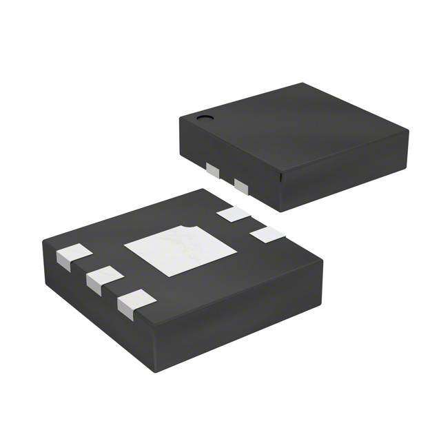
| 产品图片 |
|
| rohs | 符合RoHS无铅 / 符合限制有害物质指令(RoHS)规范要求 |
| 产品系列 | 二极管与整流器,TVS二极管,TVS二极管阵列,Littelfuse SLVU2.8-4BTGSLVU2.8-4, SPA® |
| 数据手册 | |
| 产品型号 | SLVU2.8-4BTG |
| 不同频率时的电容 | 2pF @ 1MHz |
| 产品培训模块 | http://www.digikey.cn/PTM/IndividualPTM.page?site=cn&lang=zhs&ptm=22970 |
| 产品种类 | TVS SCR/Diode Arrays |
| 供应商器件封装 | 8-SOIC |
| 其它名称 | F4206TR |
| 击穿电压 | 3 V |
| 功率-峰值脉冲 | 600W |
| 包装 | 带卷 (TR) |
| 单向通道 | - |
| 双向通道 | 4 |
| 商标 | Littelfuse |
| 安装类型 | 表面贴装 |
| 安装风格 | SMD/SMT |
| 封装 | Reel |
| 封装/外壳 | 8-SOIC(0.154",3.90mm 宽) |
| 封装/箱体 | SOIC-8 |
| 尺寸 | 4 mm W x 5 mm L x 1.75 mm H |
| 峰值浪涌电流 | 40 A |
| 峰值脉冲功率耗散 | 600 W |
| 工作温度 | -40°C ~ 125°C |
| 工作电压 | 2.8 V |
| 工厂包装数量 | 2500 |
| 应用 | 通用 |
| 最大工作温度 | + 85 C |
| 最小工作温度 | - 40 C |
| 标准包装 | 2,500 |
| 电压-击穿(最小值) | 3V |
| 电压-反向关态(典型值) | 2.8V (最小值) |
| 电压-箝位(最大值)@Ipp | 15V |
| 电流-峰值脉冲(10/1000µs) | 40A (8/20µs) |
| 电源线路保护 | 无 |
| 端接类型 | SMD/SMT |
| 类型 | 齐纳 |
| 系列 | SLVU2.8 |
| 通道 | 4 Channels |
| 钳位电压 | 15 V |
| 零件号别名 | SPLV2.8-4BTG |


- 商务部:美国ITC正式对集成电路等产品启动337调查
- 曝三星4nm工艺存在良率问题 高通将骁龙8 Gen1或转产台积电
- 太阳诱电将投资9.5亿元在常州建新厂生产MLCC 预计2023年完工
- 英特尔发布欧洲新工厂建设计划 深化IDM 2.0 战略
- 台积电先进制程称霸业界 有大客户加持明年业绩稳了
- 达到5530亿美元!SIA预计今年全球半导体销售额将创下新高
- 英特尔拟将自动驾驶子公司Mobileye上市 估值或超500亿美元
- 三星加码芯片和SET,合并消费电子和移动部门,撤换高东真等 CEO
- 三星电子宣布重大人事变动 还合并消费电子和移动部门
- 海关总署:前11个月进口集成电路产品价值2.52万亿元 增长14.8%


PDF Datasheet 数据手册内容提取
TVS Diode Arrays (SPA® Diodes) Lightning Surge Protection - SLVU2.8-4 Series SLVU2.8-4 Series 2.8V 40A TVS Array RoHS Pb GREEN Description The SLVU2.8-4 was designed to protect low voltage, CMOS devices from ESD and lightning induced transients. There is a compensating diode in series with each low voltage TVS to present a low loading capacitance to the line being protected. These robust structures can safely absorb repetitive ESD strikes at ±30kV (contact discharge) per IEC 61000-4-2 standard and each structure can safely dissipate up to 40A (IEC 61000-4-5 2nd edition, t =8/20μs) with very P low clamping voltages. Features • ESD, IEC 61000-4-2, • SOIC-8 (JEDEC MO-012) Pinout ±30kV contact, ±30kV air pin configuration allows 4 3 2 1 • EFT, IEC 61000-4-4, 40A for simple flow-through (5/50ns) layout • Lightning, IEC 61000-4-5 • RoHS Compliant and 2nd edition, 40A (8/20μs) Lead Free • Low capacitance of 2pF • Moisture Sensitivity Level per line (MSL-1) • Low leakage current of 1μA (MAX) at 2.8V 5 6 7 8 Applications • 10/100/1000 Ethernet • Analog Inputs Functional Block Diagram • WAN/LAN Equipment • Base Stations • Switching Systems Pin 1.3 Pin 6.8 • Desktops, Servers, and Notebooks Application Example RJ-45 Ethernet Connector PHY Pin 2.4 Pin 5.7 J1 Tx+ Tx- Rx+ Rx- Additional Information SLVU2.8-4 Device is shown as transparent for actual footprint Resources Samples J8 Case GND © 2017 Littelfuse, Inc. Specifications are subject to change without notice. Revised: 05/12/17
TVS Diode Arrays (SPA® Diodes) Lightning Surge Protection - SLVU2.8-4 Series Electrical Characteristics (T = 25°C) OP Parameter Symbol Test Conditions Min Typ Max Units Reverse Standoff Voltage V I ≤1μA 2.8 V RWM R Reverse Breakdown Voltage V I=2μA 3.0 V BR T Snap Back Voltage V I=50mA 2.8 V SB T Reverse Leakage Current I V =2.8V (Each Line) 1 μA LEAK R Clamping Voltage1 V I =5A, t =8/20μs (Each Line) 7.0 8.5 V C PP P Clamping Voltage1 V I =24A, t =8/20μs (Each Line) 13.9 15.0 V C PP P IEC61000-4-2 (Contact) ±30 kV ESD Withstand Voltage1 V ESD IEC61000-4-2 (Air) ±30 kV Dynamic Resistance R (V - V ) / (I - I ) (Each Line) 0.4 Ω DYN C2 C1 PP2 PP1 Diode Capacitance1 CD VR=0V, f=1MHz (Each Line) 2.0 2.5 pF Note: 1Parameter is guaranteed by design and/or device characterization. Absolute Maximum Ratings Figure 1: Capacitance vs. Reverse Voltage Parameter Rating Units 4.0 Peak Pulse Power (t =8/20µs) 600 W P 3.5 Peak Pulse Current (t =8/20µs) 40 A P Operating Temperature –40 to 125 ºC pF) 3.0 Storage Temperature –55 to 150 ºC e ( 2.5 c n a 2.0 CAUTION: Stresses above those listed in “Absolute Maximum Ratings” may cause t permanent damage to the device. This is a stress only rating and operation of the device aci 1.5 at these or any other conditions above those indicated in the operational sections of this p a specification is not implied. C 1.0 0.5 0.0 0.0 0.5 1.0 1.5 2.0 2.5 DC Bias (V) Figure 2: Clamping Voltage vs. I Figure 3: 8/20 µs Pulse Waveform PP 14 110% 100% 12 90% V) 80% g Voltage-V(C 1680 Percent of IPP 3456700000%%%%% n pi 4 20% m 10% a Cl 2 0% 0.0 5.0 10.0 15.0 20.0 25.0 30.0 0 Time (μs) 0 5 10 15 20 25 Peak Pulse Current-I (A) PP © 2017 Littelfuse, Inc. Specifications are subject to change without notice. Revised: 05/12/17
TVS Diode Arrays (SPA® Diodes) Lightning Surge Protection - SLVU2.8-4 Series Product Characteristics Soldering Parameters Reflow Condition Pb – Free assembly Lead Plating Matte Tin - Temperature Min (T ) 150°C s(min) Lead Material Copper Alloy Pre Heat - Temperature Max (T ) 200°C s(max) Lead Coplanarity 0.0004 inches (0.102mm) - Time (min to max) (t) 60 – 180 secs s Average ramp up rate (Liquidus) Temp Substitute Material Silicon 5°C/second max (T) to peak L Body Material V-0 per UL 94 Molded Epoxy T to T - Ramp-up Rate 5°C/second max S(max) L Notes : - Temperature (T) (Liquidus) 217°C 1. All dimensions are in millimeters Reflow L 2. Dimensions include solder plating. - Temperature (tL) 60 – 150 seconds 3. Dimensions are exclusive of mold flash & metal burr. 4. All specifications comply to JEDEC SPEC MO-203 Issue A Peak Temperature (TP) 260+0/-5 °C 5. Blo is facing up for mold and facing down for trim/form, i.e. reverse trim/form. Time within 5°C of actual peak 6. Package surface matte finish VDI 11-13. 20 – 40 seconds Temperature (t ) p Ramp-down Rate 5°C/second max Time 25°C to peak Temperature (T ) 8 minutes Max. P Do not exceed 260°C Package Dimensions — Mechanical Drawings and Recommended Solder Pad Outline Package SOIC-8 Pins 8 JEDEC MS-012 Millimetres Inches LF Min Max Min Max A 1.35 1.75 0.053 0.069 o A1 0.10 0.25 0.004 0.010 Recommended A2 1.25 1.65 0.050 0.065 Soldering Pad Outline (Reference Only) B 0.31 0.51 0.012 0.020 c 0.17 0.25 0.007 0.010 D 4.80 5.00 0.189 0.197 E 5.80 6.20 0.228 0.244 E1 3.80 4.00 0.150 0.157 e 1.27 BSC 0.050 BSC L 0.40 1.27 0.016 0.050 © 2017 Littelfuse, Inc. Specifications are subject to change without notice. Revised: 05/12/17
TVS Diode Arrays (SPA® Diodes) Lightning Surge Protection - SLVU2.8-4 Series Part Numbering System Part Marking System U2.8-4 SLVU2.8 -4BT G U2.8-4 PVrooUdl t=ua ScgLteV SU L2ee.r8vieesl No. of channels G= Green T= Tape & Reel Package B = SOIC-8 Series No. of channels Ordering Information Part Number Package Marking Min. Order Qty. SLVU2.8-4BTG SOIC-8 U2.8-4 2500 Embossed Carrier Tape & Reel Specification — SOIC Package Millimetres Inches User Feeding Direction Symbol Min Max Min Max E 1.65 1.85 0.065 0.073 F 5.4 5.6 0.213 0.22 P2 1.9 2.1 0.075 0.083 Pin 1 Location D 1.5 1.6 0.059 0.063 D1 1.50 Min 0.059 Min P0 3.9 4.1 0.154 0.161 10P0 40.0 ± 0.20 1.574 ± 0.008 W 11.9 12.1 0.468 0.476 P 7.9 8.1 0.311 0.319 A0 6.3 6.5 0.248 0.256 B0 5.1 5.3 0.2 0.209 K0 2 2.2 0.079 0.087 t 0.30 ± 0.05 0.012 ± 0.002 Disclaimer Notice - Information furnished is believed to be accurate and reliable. However, users should independently evaluate the suitability of and test each product selected for their own applications. Littelfuse products are not designed for, and may not be used in, all applications. Read complete Disclaimer Notice at www.littelfuse.com/disclaimer-electronics. © 2017 Littelfuse, Inc. Specifications are subject to change without notice. Revised: 05/12/17