
 Datasheet下载
- 型号: SM8S30AHE3/2D
- 制造商: Vishay
- 库位|库存: xxxx|xxxx
- 要求:
| 数量阶梯 | 香港交货 | 国内含税 |
| +xxxx | $xxxx | ¥xxxx |
查看当月历史价格
查看今年历史价格
SM8S30AHE3/2D产品简介:
ICGOO电子元器件商城为您提供SM8S30AHE3/2D由Vishay设计生产,在icgoo商城现货销售,并且可以通过原厂、代理商等渠道进行代购。 SM8S30AHE3/2D价格参考。VishaySM8S30AHE3/2D封装/规格:TVS - 二极管, 48.4V Clamp 136A Ipp Tvs Diode Surface Mount DO-218AB。您可以下载SM8S30AHE3/2D参考资料、Datasheet数据手册功能说明书,资料中有SM8S30AHE3/2D 详细功能的应用电路图电压和使用方法及教程。
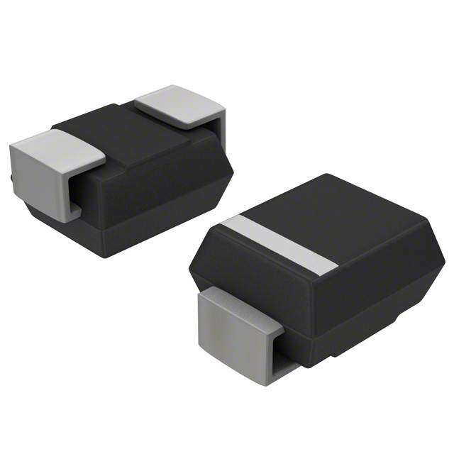
Vishay Semiconductor Diodes Division生产的TVS二极管型号SM8S30AHE3/2D,是一款高功率瞬态电压抑制二极管,主要用于保护电子电路免受瞬态过电压(如雷击、电感负载切换、静电放电等)的损害。该器件具有30V的反向工作电压和高达8000W的峰值脉冲功率,响应速度快(皮秒级),能迅速钳位过电压,保护下游敏感元件。

典型应用场景包括:

1. 工业电源系统:用于保护PLC、变频器、工控电源模块等设备中的直流总线和接口电路;
2. 汽车电子:适用于车载电源系统、电机控制单元、LED照明驱动等,符合AEC-Q101车规标准,具备良好的可靠性和耐温性;
3. 通信设备:在基站电源、以太网供电(PoE)、数据接口中提供浪涌防护;
4. 消费类电源适配器与充电器:用于AC-DC转换器输出端的过压保护;
5. 可再生能源系统:如太阳能逆变器中的直流侧保护。

SM8S30AHE3/2D采用DO-218AB封装,体积小、散热好,适合紧凑型设计,广泛应用于需要高可靠性及强抗浪涌能力的场合。其双向结构可同时抑制正负向瞬态电压,增强了系统的整体防护能力。
| 参数 | 数值 |
| 产品目录 | |
| 描述 | TVS DIODE 30VWM 53.5VC DO218ABTVS 二极管 - 瞬态电压抑制器 8.0W 30V 5% Unidir |
| 产品分类 | |
| 品牌 | Vishay SemiconductorsVishay Semiconductor Diodes Division |
| 产品手册 | |
| 产品图片 |
|
| rohs | RoHS 合规性豁免无铅 / 符合限制有害物质指令(RoHS)规范要求 |
| 产品系列 | 二极管与整流器,TVS二极管,TVS 二极管 - 瞬态电压抑制器,Vishay Semiconductors SM8S30AHE3/2DPAR® |
| 数据手册 | |
| 产品型号 | SM8S30AHE3/2DSM8S30AHE3/2D |
| 不同频率时的电容 | - |
| 产品种类 | TVS 二极管 - 瞬态电压抑制器 |
| 供应商器件封装 | DO-218AB |
| 其它名称 | SM8S30AHE3/2DGIDKR |
| 击穿电压 | 33.3 V |
| 功率-峰值脉冲 | 6600W (6.6kW) |
| 包装 | Digi-Reel® |
| 单向通道 | 1 |
| 双向通道 | - |
| 商标 | Vishay Semiconductors |
| 商标名 | PAR |
| 安装类型 | 表面贴装 |
| 安装风格 | SMD/SMT |
| 封装 | Reel |
| 封装/外壳 | DO-218AB |
| 封装/箱体 | DO-218AB |
| 尺寸 | 8.7(Max) mm W x 13.7 mm L |
| 峰值浪涌电流 | 136 A |
| 峰值脉冲功率耗散 | 6.6 kW |
| 工作温度 | -55°C ~ 175°C |
| 工作电压 | 30 V |
| 工厂包装数量 | 750 |
| 应用 | 通用 |
| 最大工作温度 | + 175 C |
| 最小工作温度 | - 55 C |
| 极性 | Unidirectional |
| 标准包装 | 1 |
| 电压-击穿(最小值) | 33.3V |
| 电压-反向关态(典型值) | 30V |
| 电压-箝位(最大值)@Ipp | 53.5V |
| 电流-峰值脉冲(10/1000µs) | 123A |
| 电源线路保护 | 无 |
| 端接类型 | SMD/SMT |
| 类型 | 齐纳 |
| 系列 | SMxSxx |
| 钳位电压 | 48.4 V |


- 商务部:美国ITC正式对集成电路等产品启动337调查
- 曝三星4nm工艺存在良率问题 高通将骁龙8 Gen1或转产台积电
- 太阳诱电将投资9.5亿元在常州建新厂生产MLCC 预计2023年完工
- 英特尔发布欧洲新工厂建设计划 深化IDM 2.0 战略
- 台积电先进制程称霸业界 有大客户加持明年业绩稳了
- 达到5530亿美元!SIA预计今年全球半导体销售额将创下新高
- 英特尔拟将自动驾驶子公司Mobileye上市 估值或超500亿美元
- 三星加码芯片和SET,合并消费电子和移动部门,撤换高东真等 CEO
- 三星电子宣布重大人事变动 还合并消费电子和移动部门
- 海关总署:前11个月进口集成电路产品价值2.52万亿元 增长14.8%


PDF Datasheet 数据手册内容提取
SM8S10 thru SM8S43A www.vishay.com Vishay General Semiconductor Surface Mount PAR® Transient Voltage Suppressors High Temperature Stability and High Reliability Conditions FEATURES • Junction passivation optimized design passivated anisotropic rectifier technology • T = 175 °C capability suitable for high reliability J and automotive requirement • Available in uni-directional polarity only • Low leakage current • Low forward voltage drop DO-218AB • High surge capability • Meets ISO7637-2 surge specification (varied by test condition) • Meets MSL level 1, per J-STD-020, LF maximum peak of 245 °C • AEC-Q101 qualified • Material categorization: for definitions of compliance PRIMARY CHARACTERISTICS please see www.vishay.com/doc?99912 V 11.1 V to 52.8 V BR TYPICAL APPLICATIONS P (10 x 1000 μs) 6600 W PPM P (10 x 10 000 μs) 5200 W Use in sensitive electronics protection against voltage PPM transients induced by inductive load switching and lighting, P 8 W D especially for automotive load dump protection application. V 10 V to 43 V WM I 700 A FSM MECHANICAL DATA T max. 175 °C J Polarity Uni-directional Case: DO-218AB Molding compound meets UL 94 V-0 flammability rating Package DO-218AB Base P/NHE3 - RoHS-compliant, AEC-Q101 qualified Base P/NHE3_X - RoHS-compliant and AEC-Q101 qualified (“X” denotes revision code e.g. A, B, ..., revision code only applicable for part number with ± 5 % tolerance) Terminals: matte tin plated leads, solderable per J-STD-002 and JESD 22-B102 HE3 suffix meets JESD 201 class 2 whisker test Polarity: heatsink is anode MAXIMUM RATINGS (T = 25 °C unless otherwise noted) C PARAMETER SYMBOL VALUE UNIT with 10/1000 μs waveform 6600 Peak pulse power dissipation P W PPM with 10/10 000 μs waveform 5200 Power dissipation on infinite heatsink at T = 25 °C (fig. 1) P 8.0 W C D Peak pulse current with 10/1000 μs waveform I (1) See next table A PPM Peak forward surge current 8.3 ms single half sine-wave I 700 A FSM Operating junction and storage temperature range T , T -55 to +175 °C J STG Note (1) Non-repetitive current pulse derated above T = 25 °C A Revision: 31-Aug-16 1 Document Number: 88387 For technical questions within your region: DiodesAmericas@vishay.com, DiodesAsia@vishay.com, DiodesEurope@vishay.com THIS DOCUMENT IS SUBJECT TO CHANGE WITHOUT NOTICE. THE PRODUCTS DESCRIBED HEREIN AND THIS DOCUMENT ARE SUBJECT TO SPECIFIC DISCLAIMERS, SET FORTH AT www.vishay.com/doc?91000
SM8S10 thru SM8S43A www.vishay.com Vishay General Semiconductor ELECTRICAL CHARACTERISTICS (T = 25 °C unless otherwise noted) C BREAKDOWN MAXIMUM MAXIMUM REVERSE MAX. PEAK MAXIMUM TEST STAND-OFF VOLTAGE REVERSE LEAKAGE PULSE CURRENT CLAMPING DEVICE CURRENT VOLTAGE V (V) LEAKAGE AT V AT 10/1000 μs VOLTAGE TYPE BR I V WM T WM AT V T = 175 °C WAVEFORM AT I MIN. MAX. (mA) (V) I (μWAM) JI (μA) (A) V P(VP)M D D C SM8S10 11.1 13.6 5.0 10.0 15 250 351 18.8 SM8S10A 11.1 12.3 5.0 10.0 15 250 388 17.0 SM8S11 12.2 14.9 5.0 11.0 10 150 328 20.1 SM8S11A 12.2 13.5 5.0 11.0 10 150 363 18.2 SM8S12 13.3 16.3 5.0 12.0 10 150 300 22.0 SM8S12A 13.3 14.7 5.0 12.0 10 150 332 19.9 SM8S13 14.4 17.6 5.0 13.0 10 150 277 23.8 SM8S13A 14.4 15.9 5.0 13.0 10 150 307 21.5 SM8S14 15.6 19.1 5.0 14.0 10 150 256 25.8 SM8S14A 15.6 17.2 5.0 14.0 10 150 284 23.2 SM8S15 16.7 20.4 5.0 15.0 10 150 245 26.9 SM8S15A 16.7 18.5 5.0 15.0 10 150 270 24.4 SM8S16 17.8 21.8 5.0 16.0 10 150 229 28.8 SM8S16A 17.8 19.7 5.0 16.0 10 150 254 26.0 SM8S17 18.9 23.1 5.0 17.0 10 150 216 30.5 SM8S17A 18.9 20.9 5.0 17.0 10 150 239 27.6 SM8S18 20.0 24.4 5.0 18.0 10 150 205 32.2 SM8S18A 20.0 22.1 5.0 18.0 10 150 226 29.2 SM8S20 22.2 27.1 5.0 20.0 10 150 184 35.8 SM8S20A 22.2 24.5 5.0 20.0 10 150 204 32.4 SM8S22 24.4 29.8 5.0 22.0 10 150 168 39.4 SM8S22A 24.4 26.9 5.0 22.0 10 150 186 35.5 SM8S24 26.7 32.6 5.0 24.0 10 150 153 43.0 SM8S24A 26.7 29.5 5.0 24.0 10 150 170 38.9 SM8S26 28.9 35.3 5.0 26.0 10 150 142 46.6 SM8S26A 28.9 31.9 5.0 26.0 10 150 157 42.1 SM8S28 31.1 38.0 5.0 28.0 10 150 132 50.1 SM8S28A 31.1 34.4 5.0 28.0 10 150 145 45.4 SM8S30 33.3 40.7 5.0 30.0 10 150 123 53.5 SM8S30A 33.3 36.8 5.0 30.0 10 150 136 48.4 SM8S33 36.7 44.9 5.0 33.0 10 150 112 59.0 SM8S33A 36.7 40.6 5.0 33.0 10 150 124 53.3 SM8S36 40.0 48.9 5.0 36.0 10 150 103 64.3 SM8S36A 40.0 44.2 5.0 36.0 10 150 114 58.1 SM8S40 44.4 54.3 5.0 40 10 150 92.4 71.4 SM8S40A 44.4 49.1 5.0 40 10 150 102 64.5 SM8S43 47.8 58.4 5.0 43 10 150 86 76.7 SM8S43A 47.8 52.8 5.0 43 10 150 95.1 69.4 Note • For all types maximum V = 1.8 V at I = 100 A measured on 8.3 ms single half sine-wave or equivalent square wave, duty cycle = 4 pulses F F per minute maximum Revision: 31-Aug-16 2 Document Number: 88387 For technical questions within your region: DiodesAmericas@vishay.com, DiodesAsia@vishay.com, DiodesEurope@vishay.com THIS DOCUMENT IS SUBJECT TO CHANGE WITHOUT NOTICE. THE PRODUCTS DESCRIBED HEREIN AND THIS DOCUMENT ARE SUBJECT TO SPECIFIC DISCLAIMERS, SET FORTH AT www.vishay.com/doc?91000
SM8S10 thru SM8S43A www.vishay.com Vishay General Semiconductor THERMAL CHARACTERISTICS (T = 25 °C unless otherwise noted) C PARAMETER SYMBOL VALUE UNIT Typical thermal resistance, junction to case R 0.90 °C/W JC ORDERING INFORMATION (Example) PREFERRED P/N UNIT WEIGHT (g) PREFERRED PACKAGE CODE BASE QUANTITY DELIVERY MODE 13" diameter plastic tape and reel, SM8S10AHE3/2D (1) 2.605 2D 750 anode towards the sprocket hole 13" diameter plastic tape and reel, SM8S10AHE3_A/I (1) 2.605 I 750 anode towards the sprocket hole Note (1) AEC-Q101 qualified RATINGS AND CHARACTERISTICS CURVES (T = 25 °C unless otherwise noted) A 8.0 150 t = 10 μs T = 25 °C r J Pulse Width (t) is d %) Defined as the Point on (W) 6.0 urrent ( 100 PIPePMak Value WDehcearey sth teo P50ea %k Couf rIrPePnMt wer Dissipati 4.0 Peak Pulse C 50 HIPaPMlf Value - IP2P Po 2.0 ut p n I t d 0 0 0 50 100 150 200 0 10 20 30 40 Case Temperature (°C) t - Time (ms) Fig. 1 - Power Derating Curve Fig. 3 - Pulse Waveform 6000 10 000 5000 W) er (W)4000 wer ( w o o P P e mp 3000 urg u S D e ad 2000 ers o v L e R 1000 0 1000 25 50 75 100 125 150 175 10 100 Case Temperature (°C) Pulse Width (ms) - ½ I Exponential Waveform PP Fig. 2 - Load Dump Power Characteristics Fig. 4 - Reverse Power Capability (10 ms Exponential Waveform) Revision: 31-Aug-16 3 Document Number: 88387 For technical questions within your region: DiodesAmericas@vishay.com, DiodesAsia@vishay.com, DiodesEurope@vishay.com THIS DOCUMENT IS SUBJECT TO CHANGE WITHOUT NOTICE. THE PRODUCTS DESCRIBED HEREIN AND THIS DOCUMENT ARE SUBJECT TO SPECIFIC DISCLAIMERS, SET FORTH AT www.vishay.com/doc?91000
SM8S10 thru SM8S43A www.vishay.com Vishay General Semiconductor 100 100 000 W) TJ = 25 °C C/ F) f = 1.0 MHz e (° 10 RθJA e (p Vsig = 50 mVp-p c c n n a a ed cit p a mal Im 1 RθJC n Cap 10 000 Measured at Zero Bias nsient Ther 0.1 C - JunctioJ Measured at Stand-Off Tra Voltage VWM 0.01 1000 0.01 0.1 1 10 100 10 15 20 25 30 35 40 45 t - Pulse Width (s) VWM - Reverse Stand-Off Voltage (V) Fig. 5 - Typical Transient Thermal Impedance Fig. 6 - Typical Junction Capacitance PACKAGE OUTLINE DIMENSIONS in inches (millimeters) DO-218AB 0.628 (16.0) 0.592 (15.0) Mounting Pad Layout 0.539 (13.7) 0.524 (13.3) 0.150 (3.8) 0.116 (3.0) 0.126 (3.2) 0.093 (2.4) 0.091 (2.3) 0.413 (10.5) 0.342 (8.7) 0.067 (1.7) 0.374 (9.5) 0.327 (8.3) 0.413 (10.5) 0.116 (3.0) 0.374 (9.5) 0.093 (2.4) 0.366 (9.3) 0.343 (8.7) 0.406 (10.3) 0.366 (9.3) 0.382 (9.7) Lead 1 0.343 (8.7) 0.606 (15.4) 0.197 (5.0) 0.583 (14.8) 0.185 (4.7) 0.138 (3.5) 0.098 (2.5) 0.098 (2.5) 0.016 (0.4) MIN. 0.059 (1.5) Lead 2/Metal Heatsink 0.028 (0.7) 0.020 (0.5) Revision: 31-Aug-16 4 Document Number: 88387 For technical questions within your region: DiodesAmericas@vishay.com, DiodesAsia@vishay.com, DiodesEurope@vishay.com THIS DOCUMENT IS SUBJECT TO CHANGE WITHOUT NOTICE. THE PRODUCTS DESCRIBED HEREIN AND THIS DOCUMENT ARE SUBJECT TO SPECIFIC DISCLAIMERS, SET FORTH AT www.vishay.com/doc?91000
Legal Disclaimer Notice www.vishay.com Vishay Disclaimer ALL PRODUCT, PRODUCT SPECIFICATIONS AND DATA ARE SUBJECT TO CHANGE WITHOUT NOTICE TO IMPROVE RELIABILITY, FUNCTION OR DESIGN OR OTHERWISE. Vishay Intertechnology, Inc., its affiliates, agents, and employees, and all persons acting on its or their behalf (collectively, “Vishay”), disclaim any and all liability for any errors, inaccuracies or incompleteness contained in any datasheet or in any other disclosure relating to any product. Vishay makes no warranty, representation or guarantee regarding the suitability of the products for any particular purpose or the continuing production of any product. To the maximum extent permitted by applicable law, Vishay disclaims (i) any and all liability arising out of the application or use of any product, (ii) any and all liability, including without limitation special, consequential or incidental damages, and (iii) any and all implied warranties, including warranties of fitness for particular purpose, non-infringement and merchantability. Statements regarding the suitability of products for certain types of applications are based on Vishay’s knowledge of typical requirements that are often placed on Vishay products in generic applications. Such statements are not binding statements about the suitability of products for a particular application. It is the customer’s responsibility to validate that a particular product with the properties described in the product specification is suitable for use in a particular application. Parameters provided in datasheets and / or specifications may vary in different applications and performance may vary over time. All operating parameters, including typical parameters, must be validated for each customer application by the customer’s technical experts. Product specifications do not expand or otherwise modify Vishay’s terms and conditions of purchase, including but not limited to the warranty expressed therein. Except as expressly indicated in writing, Vishay products are not designed for use in medical, life-saving, or life-sustaining applications or for any other application in which the failure of the Vishay product could result in personal injury or death. Customers using or selling Vishay products not expressly indicated for use in such applications do so at their own risk. Please contact authorized Vishay personnel to obtain written terms and conditions regarding products designed for such applications. No license, express or implied, by estoppel or otherwise, to any intellectual property rights is granted by this document or by any conduct of Vishay. Product names and markings noted herein may be trademarks of their respective owners. Revision: 13-Jun-16 1 Document Number: 91000