 Datasheet下载
- 型号: ESDA6V1L
- 制造商: STMicroelectronics
- 库位|库存: xxxx|xxxx
- 要求:
| 数量阶梯 | 香港交货 | 国内含税 |
| +xxxx | $xxxx | ¥xxxx |
查看当月历史价格
查看今年历史价格
ESDA6V1L产品简介:
ICGOO电子元器件商城为您提供ESDA6V1L由STMicroelectronics设计生产,在icgoo商城现货销售,并且可以通过原厂、代理商等渠道进行代购。 ESDA6V1L价格参考¥1.12-¥4.94。STMicroelectronicsESDA6V1L封装/规格:TVS - 二极管, Clamp Ipp Tvs Diode Surface Mount SOT-23-3。您可以下载ESDA6V1L参考资料、Datasheet数据手册功能说明书,资料中有ESDA6V1L 详细功能的应用电路图电压和使用方法及教程。
STMicroelectronics(意法半导体)的ESDA6V1L是一款瞬态电压抑制(TVS)二极管,属于ESD保护器件,主要用于电子设备中防止静电放电(ESD)和瞬态电压脉冲对敏感电路造成损害。该器件为单向TVS二极管,工作电压为6.1V,具有低电容特性(典型值约3pF),适用于高速信号线路的保护。

典型应用场景包括:

1. 消费类电子产品:广泛应用于智能手机、平板电脑、笔记本电脑等设备中的数据接口保护,如USB、HDMI、音频接口等,防止用户使用过程中因静电导致芯片损坏。

2. 通信接口保护:用于保护RS-232、I²C、UART等低电压信号线,确保通信稳定可靠。

3. 便携式设备:由于其小型化封装(如SOD-323),非常适合空间受限的便携设备,兼顾高性能与紧凑布局需求。

4. 工业与家电控制板:在微控制器单元(MCU)、传感器接口等部位提供ESD防护,提升系统可靠性。

5. 汽车电子:适用于车载信息娱乐系统、导航设备等非动力系统的低压电路,满足AEC-Q101可靠性标准的部分要求。

ESDA6V1L具备快速响应时间、高脉冲承受能力(可满足IEC 61000-4-2 Level 4 ±8kV接触放电要求),是保护现代低压、高速电子系统免受瞬态干扰的理想选择。
| 参数 | 数值 |
| 产品目录 | |
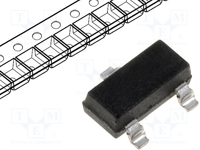
| 描述 | TVS DIODE 5.25VWM SOT23TVS二极管阵列 6.1V 300W Unidirect |
| 产品分类 | |
| 品牌 | STMicroelectronics |
| 产品手册 | |
| 产品图片 |
|
| rohs | 符合RoHS无铅 / 符合限制有害物质指令(RoHS)规范要求 |
| 产品系列 | 二极管与整流器,TVS二极管,TVS二极管阵列,STMicroelectronics ESDA6V1LESDA, TRANSIL™ |
| 数据手册 | |
| 产品型号 | ESDA6V1L |
| 不同频率时的电容 | - |
| 产品目录页面 | |
| 产品种类 | TVS二极管阵列 |
| 供应商器件封装 | SOT-23-3 |
| 其它名称 | 497-2930-6 |
| 其它有关文件 | http://www.st.com/web/catalog/sense_power/FM114/CL1137/SC492/PF74298?referrer=70071840http://www.st.com/web/catalog/sense_power/FM114/CL1137/SC492/SS1421/PF74298?referrer=70071840 |
| 击穿电压 | 6.1 V |
| 功率-峰值脉冲 | 300W |
| 包装 | Digi-Reel® |
| 单向通道 | 2 |
| 双向通道 | - |
| 商标 | STMicroelectronics |
| 商标名 | Transil |
| 安装类型 | 表面贴装 |
| 安装风格 | SMD/SMT |
| 封装 | Reel |
| 封装/外壳 | TO-236-3,SC-59,SOT-23-3 |
| 封装/箱体 | SOT-23 |
| 尺寸 | 2.75 mm W x 3.04 mm L x 1.6 mm H |
| 峰值脉冲功率耗散 | 300 W |
| 工作温度 | -40°C ~ 125°C (TJ) |
| 工作电压 | 5.25 V |
| 工厂包装数量 | 3000 |
| 应用 | 通用 |
| 最大工作温度 | + 125 C |
| 最小工作温度 | - 40 C |
| 极性 | Bidirectional |
| 标准包装 | 1 |
| 电压-击穿(最小值) | 6.1V |
| 电压-反向关态(典型值) | 5.25V |
| 电压-箝位(最大值)@Ipp | - |
| 电容 | 140 pF |
| 电流-峰值脉冲(10/1000µs) | - |
| 电源线路保护 | 无 |
| 端接类型 | SMD/SMT |
| 类型 | 齐纳 |
| 系列 | ESDAL |
| 通道 | 2 Channels |


- 商务部:美国ITC正式对集成电路等产品启动337调查
- 曝三星4nm工艺存在良率问题 高通将骁龙8 Gen1或转产台积电
- 太阳诱电将投资9.5亿元在常州建新厂生产MLCC 预计2023年完工
- 英特尔发布欧洲新工厂建设计划 深化IDM 2.0 战略
- 台积电先进制程称霸业界 有大客户加持明年业绩稳了
- 达到5530亿美元!SIA预计今年全球半导体销售额将创下新高
- 英特尔拟将自动驾驶子公司Mobileye上市 估值或超500亿美元
- 三星加码芯片和SET,合并消费电子和移动部门,撤换高东真等 CEO
- 三星电子宣布重大人事变动 还合并消费电子和移动部门
- 海关总署:前11个月进口集成电路产品价值2.52万亿元 增长14.8%


PDF Datasheet 数据手册内容提取
ESDAL Dual Transil™ array for ESD protection Datasheet - production data Applications Where transient overvoltage protection in ESD sensitive equipment is required, such as: Entertainment Signal communications Connectivity Comfort and convenience Description SOT23-3L This device is a diode array designed to protect 1 line or 2 lines against ESD transients. The device is ideal for applications where both reduced line capacitance and board space saving Features are required. Unidirectional device It can also be used as bidirectional suppressor by Low leakage current (I max. < 20 µA at R connecting only pin 1 and 2. V ) BR 300 W peak pulse power (8/20 µs) Figure 1: Functional diagram Benefits High ESD protection level: up to 30 kV 1 High integration Suitable for high density boards Complies with the following 3 standards IEC 61000-4-2 (exceeds level 4) : 2 30 kV (air discharge) 30 kV (contact discharge) July 2017 DocID7058 Rev 5 1/11 This is information on a product in full production. www.st.com
Characteristics ESDAL 1 Characteristics Table 1: Absolute maximum ratings (Tamb = 25 °C) Symbol Parameter Value Unit IEC 61000-4-2: Vpp Peak pulse voltage(1) Contact discharge 30 kV Air discharge 30 Ppp Peak pulse power (8/20 μs) 300 W ESDA5V3L 25 ESDA6V1L 18 Ipp Peak pulse current (8/20 μs) ESDA14V2L 14 A ESDA25L 7 ESDA37L 6.3 Tj Operating junction temperature range -40 to 150 °C Tstg Storage junction temperature range -65 to 150 °C Maximum lead temperature for soldering during 10 s at 5 mm from TL case 260 °C Notes: (1)For a surge greater than the maximum values, the diode will fail in short-circuit. Figure 2: Electrical characteristics (definitions) I Symbol Parameter V = Breakdownvoltage IF BR V = Clampingvoltage CL V = Stand-offvoltage RM IRM = Leakagecurrent VBR VF I = Forwardcurrent Vcl VRM F V I = Peakpulsecurrent IRM PP I = Breakdowncurrent R V = Forwardvoltagedrop F C = Capacitance R = Dynamicimpedance Slope=1/Rd d IPP αT = Voltagetemperature 2/11 DocID7058 Rev 5
ESDAL Characteristics Table 2: Electrical characteristics (Tamb = 25 °C) VBR at IR IRM at VRM Rd(1) αT(2) Cline VF at IF Order code Min. Max. Max. Typ. Max. Typ. at 0 V bias Max. V V mA µA V mΩ 10-4/°C pF V mA ESDA5V3L 5.3 5.9 1 2 3 280 5 220 1.25 200 ESDA6V1L 6.1 7.2 1 20 5.25 350 6 140 1.25 200 ESDA14V2L 14.2 15.8 1 5 12 650 10 90 1.25 200 ESDA25L 25 30 1 1 24 1000 10 50 1.2 10 ESDA37L 37 43.3 1 1 36 2400 10 48 0.9 10 Notes: (1)Square pulse Ipp = 15 A, tp = 2.5 µs (2)∆ VBR = αT x (Tamb -25 °C) x VBR (25 °C) DocID7058 Rev 5 3/11
Characteristics ESDAL 1.1 Characteristics (curves) Figure 4: Peak pulse power versus exponential Figure 3: Variation of peak pulse power versus pulse duration initial junction temperature PPP(W) PPP(W) Tjinitial=25°C 350 maximumvalue 1000 300 250 200 150 100 100 50 Tj(°C) 0 25 50 75 100 125 150 175 tp(µs) ESDA5V3LESDA6V1LESDA14V2LESDA25L ESDA37L 10 10 100 1000 Figure 5: Variation of clamping voltage versus Figure 6: Relative variation of leakage current peak pulse current (max. values, 8/20 µs waveform) at VR = VRM versus junction values IPP(A) Ir(nA) 100 10000 Tjini8ti/a2l0=µs25°C ESDA5V3L ESDA6V1L 1000 ESDA14V2L ESDA25L 10 ESDA37L 100 10 1 1 ESDA5V3L ESDA6V1L 0.1 ESDA14V2L ESDA25L VCL(V) Tj(°C) ESDA37L 0.1 0.01 0 10 20 30 40 50 60 25 50 75 100 125 150 4/11 DocID7058 Rev 5
ESDAL Application and design guidelines 2 Application and design guidelines Refer to STMicroelectronics application note: AN2689: Protection of automotive electronics from electrical hazards, guidelines for design and component selection. DocID7058 Rev 5 5/11
Package information ESDAL 3 Package information In order to meet environmental requirements, ST offers these devices in different grades of ECOPACK® packages, depending on their level of environmental compliance. ECOPACK® specifications, grade definitions and product status are available at: www.st.com. ECOPACK® is an ST trademark. Epoxy meets UL 94,V0 Lead-free package 3.1 SOT23-3L mechanical data Figure 7: SOT23-3L package outline 0053390_I 6/11 DocID7058 Rev 5
ESDAL Package information Table 3: SOT23-3L mechanical data mm Dim. Min. Typ. Max. A 0.89 1.40 A1 0 0.10 B 0.30 0.51 C 0.085 0.18 D 2.75 3.04 e 0.85 1.05 e1 1.70 2.10 E 1.20 1.75 H 2.10 3.00 L 0.60 S 0.35 0.65 L1 0.25 0.55 a 0° 8° Figure 8: SOT23-3L recommended footprint Dimensions are in mm. DocID7058 Rev 5 7/11
Recommendation on PCB assembly ESDAL 4 Recommendation on PCB assembly 4.1 Solder paste 1. Halide-free flux qualification ROL0 according to ANSI/J-STD-004. 2. “No clean” solder paste is recommended. 3. Offers a high tack force to resist component movement during high speed. 4. Use solder paste with fine particles: powder particle size 20-45 µm. 4.2 Placement 1. Manual positioning is not recommended. 2. It is recommended to use the lead recognition capabilities of the placement system, not the outline centering 3. Standard tolerance of ±0.05 mm is recommended. 4. 3.5 N placement force is recommended. Too much placement force can lead to squeezed out solder paste and cause solder joints to short. Too low placement force can lead to insufficient contact between package and solder paste that could cause open solder joints or badly centered packages. 5. To improve the package placement accuracy, a bottom side optical control should be performed with a high resolution tool. 6. For assembly, a perfect supporting of the PCB (all the more on flexible PCB) is recommended during solder paste printing, pick and place and reflow soldering by using optimized tools. 4.3 PCB design preference 1. To control the solder paste amount, the closed via is recommended instead of open vias. 2. The position of tracks and open vias in the solder area should be well balanced. A symmetrical layout is recommended, to avoid any tilt phenomena caused by asymmetrical solder paste due to solder flow away. 8/11 DocID7058 Rev 5
ESDAL Recommendation on PCB assembly 4.4 Reflow profile Figure 9: ST ECOPACK® recommended soldering reflow profile for PCB mounting Minimize air convection currents in the reflow oven to avoid component movement. DocID7058 Rev 5 9/11
Ordering information ESDAL 5 Ordering information Figure 10: Ordering information scheme ESDA XXX L ESDArray Minimum breakdown voltage Package L = SOT23-3L Table 3: Ordering information Order code Marking(1) Package Weight Base qty. Delivery mode ESDA5V3L EL53 ESDA6V1L EL61 8.7 mg ESDA14V2L EL15 SOT23-3L 3000 Tape and reel ESDA25L EL25 ESDA37L EL37 9.8 mg Notes: (1)The marking can be rotated by multiples of 90° to differentiate assembly location. 6 Revision history Table 4: Document revision history Date Revision Changes 31-Jul-2012 4 First issue. 20-Jul-2017 5 Added ESDA37L package information. 10/11 DocID7058 Rev 5
ESDAL IMPORTANT NOTICE – PLEASE READ CAREFULLY STMicroelectronics NV and its subsidiaries (“ST”) reserve the right to make changes, corrections, enhancements, modifications, and improvements to ST products and/or to this document at any time without notice. Purchasers should obtain the latest relevant information on ST products before placing orders. ST products are sold pursuant to ST’s terms and conditions of sale in place at the time of order acknowledgement. Purchasers are solely responsible for the choice, selection, and use of ST products and ST assumes no liability for application assistance or the design of Purchasers’ products. No license, express or implied, to any intellectual property right is granted by ST herein. Resale of ST products with provisions different from the information set forth herein shall void any warranty granted by ST for such product. ST and the ST logo are trademarks of ST. All other product or service names are the property of their respective owners. Information in this document supersedes and replaces information previously supplied in any prior versions of this document. © 2017 STMicroelectronics – All rights reserved DocID7058 Rev 5 11/11