 Datasheet下载
- 型号: SM6T30A
- 制造商: STMicroelectronics
- 库位|库存: xxxx|xxxx
- 要求:
| 数量阶梯 | 香港交货 | 国内含税 |
| +xxxx | $xxxx | ¥xxxx |
查看当月历史价格
查看今年历史价格
SM6T30A产品简介:
ICGOO电子元器件商城为您提供SM6T30A由STMicroelectronics设计生产,在icgoo商城现货销售,并且可以通过原厂、代理商等渠道进行代购。 SM6T30A价格参考。STMicroelectronicsSM6T30A封装/规格:TVS - 二极管, 。您可以下载SM6T30A参考资料、Datasheet数据手册功能说明书,资料中有SM6T30A 详细功能的应用电路图电压和使用方法及教程。
SM6T30A 是由 STMicroelectronics(意法半导体)生产的一款 TVS(瞬态电压抑制器)二极管,属于 SM6 系列。它主要用于保护电子设备免受瞬态电压尖峰的损害,例如静电放电 (ESD)、雷击感应浪涌和开关噪声等。

 应用场景:

1. 电源线保护
   SM6T30A 可用于交流或直流电源输入端口的保护,防止因雷击或其他外部干扰引起的电压浪涌对电路造成损坏。其高浪涌电流承受能力(最高可达 1500W/10ms)使其非常适合工业和家用电器的电源保护。

2. 通信接口保护
   在 RS-232、RS-485、USB 或以太网等通信接口中,SM6T30A 能有效抑制信号线上的瞬态电压,确保数据传输的稳定性和可靠性。特别适用于需要长时间稳定运行的工业通信设备。

3. 汽车电子系统
   在汽车电子中,该器件可用于保护车载信息娱乐系统、传感器模块和 CAN 总线等关键部件。其工作电压范围(30V)适合许多汽车电子应用,并能应对复杂的电磁环境。

4. 消费类电子产品
   对于手机充电器、笔记本电脑适配器和其他便携式设备,SM6T30A 提供了高效的 ESD 和浪涌保护功能,延长产品的使用寿命并提高安全性。

5. 工业控制设备
   在工厂自动化设备、PLC(可编程逻辑控制器)和变频器中,SM6T30A 能够抵御恶劣环境下产生的电压尖峰,保障设备的正常运行。

6. 太阳能逆变器与储能系统
   在新能源领域,SM6T30A 可用于保护光伏逆变器和电池管理系统中的敏感组件,避免因外部干扰导致的故障。

总结来说,SM6T30A 凭借其出色的性能参数和可靠性,广泛应用于各种需要瞬态电压保护的场合,尤其是在电源、通信、汽车和工业领域中发挥重要作用。
| 参数 | 数值 |
| 产品目录 | |
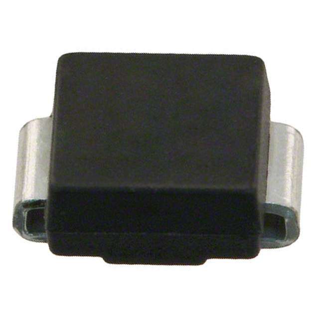
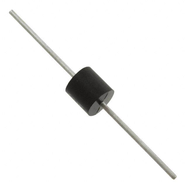
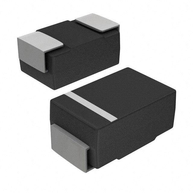
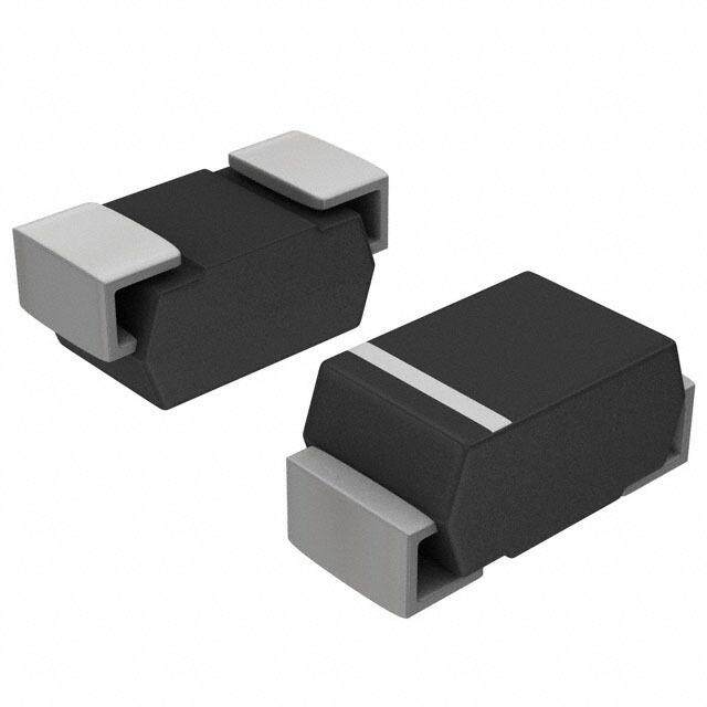
| 描述 | TVS DIODE 25.6VWM 53.5VC SMBTVS 二极管 - 瞬态电压抑制器 600W 30V Unidirect |
| 产品分类 | |
| 品牌 | STMicroelectronics |
| 产品手册 | |
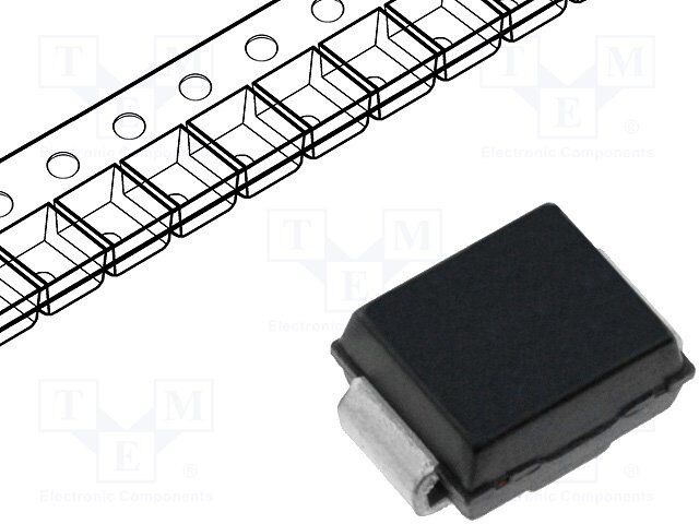
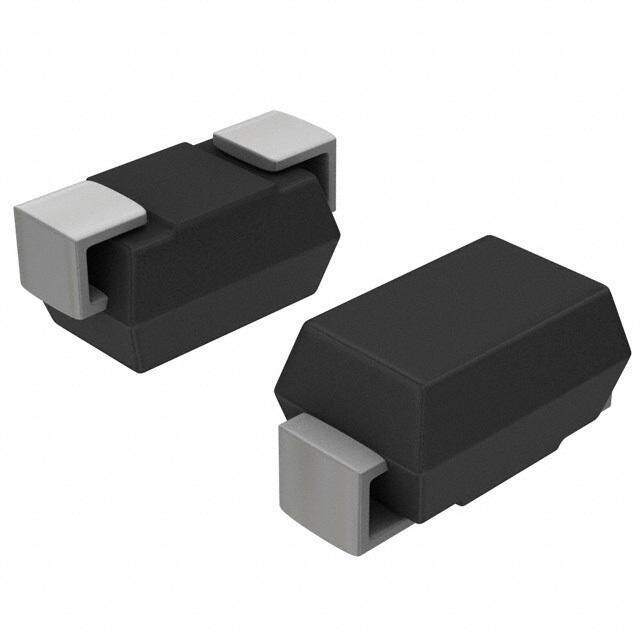
| 产品图片 |
|
| rohs | 符合RoHS无铅 / 符合限制有害物质指令(RoHS)规范要求 |
| 产品系列 | 二极管与整流器,TVS二极管,TVS 二极管 - 瞬态电压抑制器,STMicroelectronics SM6T30ASM6T, TRANSIL™ |
| 数据手册 | |
| 产品型号 | SM6T30A |
| 不同频率时的电容 | - |
| 产品目录页面 | |
| 产品种类 | TVS 二极管 - 瞬态电压抑制器 |
| 供应商器件封装 | SMB (DO-214AA) |
| 其它名称 | 497-7437-1 |
| 其它有关文件 | http://www.st.com/web/catalog/sense_power/FM114/CL1460/SC234/PF64210?referrer=70071840 |
| 击穿电压 | 28.5 V to 31.5 V |
| 功率-峰值脉冲 | 600W |
| 包装 | 剪切带 (CT) |
| 单向通道 | 1 |
| 双向通道 | - |
| 商标 | STMicroelectronics |
| 商标名 | Transil |
| 安装类型 | 表面贴装 |
| 安装风格 | SMD/SMT |
| 封装 | Reel |
| 封装/外壳 | DO-214AA,SMB |
| 封装/箱体 | DO-214AA |
| 尺寸 | 3.95 mm W x 4.6 mm L x 2.45 mm H |
| 峰值浪涌电流 | 75 A |
| 峰值脉冲功率耗散 | 600 W |
| 工作温度 | -55°C ~ 150°C |
| 工作电压 | 25.6 V |
| 工厂包装数量 | 2500 |
| 应用 | 通用 |
| 最大工作温度 | + 150 C |
| 最小工作温度 | - 55 C |
| 极性 | Unidirectional |
| 标准包装 | 1 |
| 特色产品 | http://www.digikey.com/cn/zh/ph/st/transil-protection-devices.html |
| 电压-击穿(最小值) | 28.5V |
| 电压-反向关态(典型值) | 25.6V |
| 电压-箝位(最大值)@Ipp | 53.5V |
| 电容 | 1075 pF |
| 电流-峰值脉冲(10/1000µs) | 75A (8/20µs) |
| 电源线路保护 | 无 |
| 端接类型 | SMD/SMT |
| 类型 | 齐纳 |
| 系列 | SM6T30 |
| 钳位电压 | 53.5 V |


- 商务部:美国ITC正式对集成电路等产品启动337调查
- 曝三星4nm工艺存在良率问题 高通将骁龙8 Gen1或转产台积电
- 太阳诱电将投资9.5亿元在常州建新厂生产MLCC 预计2023年完工
- 英特尔发布欧洲新工厂建设计划 深化IDM 2.0 战略
- 台积电先进制程称霸业界 有大客户加持明年业绩稳了
- 达到5530亿美元!SIA预计今年全球半导体销售额将创下新高
- 英特尔拟将自动驾驶子公司Mobileye上市 估值或超500亿美元
- 三星加码芯片和SET,合并消费电子和移动部门,撤换高东真等 CEO
- 三星电子宣布重大人事变动 还合并消费电子和移动部门
- 海关总署:前11个月进口集成电路产品价值2.52万亿元 增长14.8%

PDF Datasheet 数据手册内容提取
SM6T Transil™ Datasheet - production data Complies with the following standards A A IEC 61000-4-2 level 4: 15 kV (air discharge) 8 kV (contact discharge) IEC 61000-4-5 K K MIL STD 883G, method 3015-7: class 3B: 25 kV HBM (human body model) UL 497B, file number: QVGQ2.E136224 Unidirectional Bidirectional SMB Resin meets UL 94, V0 (JEDECDO-214AA) MIL-STD-750, method 2026 solderability EIA STD RS-481 and IEC 60286-3 packing IPC 7531 footprint Features Description Peak pulse power: The SM6T Transil series are designed to protect 600 W (10/1000 μs) sensitive equipment against electrostatic 4 kW (8/20 μs) discharges according to IEC 61000-4-2 and MIL Stand-off voltage range: from 6.8 V to 220 V STD 883, method 3015, and electrical overstress Unidirectional and bidirectional types according to IEC 61000-4-4 and 5. These Low leakage current: devices are more generally used against surges 0.2 μA at 25 °C below 600 W (10/1000 μs). 1 μA at 85 °C Operating T max: 150 °C The Planar technology makes it suitable for high- j High power capability at T max.: end equipment and SMPS where low leakage j current and high junction temperature are 515 W (10/1000 µs) required to provide reliability and stability over JEDEC registered package outline time. SM6T are packaged in SMB (SMB footprint in accordance with IPC 7531 standard). January 2018 DocID3082 Rev 10 1/11 This is information on a product in full production. www.st.com
Characteristics SM6T 1 Characteristics Table 1: Absolute maximum ratings (Tamb = 25 °C) Symbol Parameter Value Unit PPP Peak pulse power dissipation(1) Tj initial = Tamb 600 W Tstg Storage temperature range -65 to +150 °C Tj Operating junction temperature range -55 to +150 °C TL Maximum lead temperature for soldering during 10 s 260 °C Notes: (1)For a surge greater than the maximum values, the diode will fail in short-circuit. Table 2: Thermal resistance Symbol Parameter Value Unit Rth(j-l) Junction to leads 20 °C/W Rth(j-a) Junction to ambient on printed circuit on recommended pad layout 100 °C/W Figure 1: Electrical characteristics - parameter definitions Figure 2: Pulse definition for electrical characteristics 2/11 DocID3082 Rev 10
SM6T Characteristics Table 3: Electrical characteristics parameter values (Tamb = 25 °C, unless otherwise specified) IRM max at VRM VBR at IR(1) 10 / 1000 µs 8 / 20µs αT(2) VCL IPP RD VCL IPP RD Order code 25 85 Min. Typ. Max. Max. Max. Max. Max. °C °C 10- µA V V mA V(3) A(4) Ω V A Ω 4/°C SM6T6V8A/CA 20 50 5.8 6.45 6.8 7.14 10 10.5 57 0.059 14.4 275 0.027 5.7 SM6T7V5A/CA 20 50 6.4 7.13 7.5 7.88 10 11.3 53 0.065 15.2 266 0.027 6.1 SM6T10A/CA 20 50 8.55 9.5 10.0 10.5 1 14.5 41 0.098 18.6 215 0.038 7.3 SM6T12A/CA 0.2 1 10.2 11.4 12 12.6 1 16.7 36 0.114 21.7 184 0.049 7.8 SM6T15A/CA 0.2 1 12.8 14.3 15 15.8 1 21.2 28 0.193 27.2 147 0.078 8.4 SM6T18A/CA 0.2 1 15.3 17.1 18 18.9 1 25.2 24 0.263 32.5 123 0.111 8.8 SM6T22A/CA 0.2 1 18.8 20.9 22 23.1 1 30.6 20 0.375 39.3 102 0.159 9.2 SM6T24A/CA 0.2 1 20.5 22.8 24 25.2 1 33.2 18 0.444 42.8 93 0.189 9.4 SM6T27A/CA 0.2 1 23.1 25.7 27 28.4 1 37.5 16 0.569 48.3 83 0.240 9.6 SM6T30A/CA 0.2 1 25.6 28.5 30 31.5 1 41.5 14.5 0.690 53.5 75 0.293 9.7 SM6T33A/CA 0.2 1 28.2 31.4 33 34.7 1 45.7 13.1 0.840 59.0 68 0.357 9.8 SM6T36A/CA 0.2 1 30.8 34.2 36 37.8 1 49.9 12 1.01 64.3 62 0.427 9.9 SM6T39A/CA 0.2 1 33.3 37.1 39 41.0 1 53.9 11.1 1.16 69.7 57 0.504 10.0 SM6T56A/CA 0.2 1 47.6 53.2 56 58.8 1 76.6 7.8 2.28 100 40 1.030 10.0 SM6T68A/CA 0.2 1 58.1 64.6 68 71.4 1 92 6.5 3.17 121 33 1.503 10.4 SM6T75A/CA 0.2 1 64.1 71.3 75 78.8 1 103 5.8 4.17 134 30 1.84 10.5 SM6T100A/CA 0.2 1 85.5 95.0 100 105 1 137 4.4 7.27 178 22.5 3.24 10.6 SM6T150A/CA 0.2 1 128 143 150 158 1 207 2.9 16.9 265 15 7.13 10.8 SM6T200A/CA 0.2 1 171 190 200 210 1 274 2.2 29.1 353 11.3 12.7 10.8 SM6T220A/CA 0.2 1 188 209 220 231 1 328 2 48.5 388 10.3 15.2 10.8 Notes: (1)Pulse test: tp < 50 ms (2)To calculate VBR or VCL versus junction temperature, use the following formulas: V at T = V at 25 °C x (1 + αT x (T - 25)) V at T = V at 25 °C x (1 + αT x (T -25)) BR J BR J CL J CL J (3)To calculate maximum clamping voltage at other surge level, use the following formula: V = V + R x I where I is the surge current in the application CLmax BR max D PPappli PPappli (4)Surge capability given for both directions for unidirectional and bidirectional types. DocID3082 Rev 10 3/11
Characteristics SM6T 1.1 Characteristics (curves) Figure 3: Peak power dissipation versus initial Figure 4: Peak pulse power versus exponential junction temperature pulse duration Ppp(W) PPP(kW) 700 100.0 Tjinitial=25°C 600 500 10.0 400 300 1.0 200 100 Tj(°C) tP(ms) 0 0.1 0 25 50 75 100 125 150 175 1.0E-03 1.0E-02 1.0E-01 1.0E+00 1.0E+01 Figure 5: Clamping voltage versus peak pulse current (maximum values) IPP(A) 1000.0 Tjinitial=25 °C 100.0 10.0 8/20 µs 10/1000 µs 1.0 A A A V8 5A 0A 8A 00 20 10ms 6 1 3 6 1 2 T T T T T T 6 6 6 6 6 6 M M M M M M VCL(V) S S S S S S 0.1 1 10 100 1000 4/11 DocID3082 Rev 10
SM6T Characteristics Figure 6: Capacitance versus reverse applied Figure 7: Capacitance versus reverse applied voltage for unidirectional types (typical values) voltage for bidirectional types (typical values) C(pF) C(pF) 10000 10000 F=1MHz F=1MHz VoscT=j=3205m°VCRMS SM6T6V8CA VoscT=j=3205m°VCRMS 1000 SM6T6V8A 1000 SM6T15CA SM6T15A SM6T30CA SM6T30A SM6T68CA 100 SM6T68A 100 SM6T100CA SM6T100A SM6T220CA 10 VR(V) SM6T220A 10 VR(V) 1 10 100 1000 1 10 100 1000 Figure 8: Peak forward voltage drop versus peak Figure 9: Relative variation of thermal impedance forward current (typical values) junction to ambient versus pulse duration Zth(j-a)/Rth(j-a) 1.0E+02 IFM(A) 1.00 Recommendedpadlayout PrintedcircuitboardFR4,copperthickness=35µm 1.0E+01 Tj=125°C 1.0E+00 Tj=25°C 0.10 1.0E-01 tp s 1.0E-02 VFM(V) 0.01 0.0 0.5 1.0 1.5 2.0 2.5 3.0 1.0E-03 1.0E-02 1.0E-01 1.0E+00 1.0E+01 1.0E+02 1.0E+03 Figure 10: Thermal resistance junction to ambient Figure 11: Leakage current versus junction versus copper surface under each lead temperature (typical values) Rth(j-a)(°C/W) IR(nA) 110 1.E+03 100 90 (cporpinpteerdthciicrckunietsbsoa=rd35FµRm4), VRVMR=<V1R0MV 1.E+02 80 70 60 1.E+01 50 40 2300 1.E+00 VVRMR=≥V1R0MV 10 SCu(cm²) Tj(°C) 0 1.E-01 0.0 0.5 1.0 1.5 2.0 2.5 3.0 3.5 4.0 4.5 5.0 25 50 75 100 125 150 DocID3082 Rev 10 5/11
Package information SM6T 2 Package information In order to meet environmental requirements, ST offers these devices in different grades of ECOPACK® packages, depending on their level of environmental compliance. ECOPACK® specifications, grade definitions and product status are available at: www.st.com. ECOPACK® is an ST trademark. Case: JEDEC DO214-AA molded plastic over planar junction Terminals: solder plated, solderable per MIL-STD-750, method 2026 Polarity: for unidirectional types the band indicates cathode. Flammability: epoxy is rated UL94V-0 RoHS package 2.1 SMB package information Figure 12: SMB package outline 6/11 DocID3082 Rev 10
SM6T Package information Table 4: SMB package mechanical data Dimensions Ref. Millimeters Inches Min. Max. Min. Max. A1 1.90 2.45 0.0748 0.0965 A2 0.05 0.20 0.0020 0.0079 b 1.95 2.20 0.0768 0.0867 c 0.15 0.40 0.0059 0.0157 D 3.30 3.95 0.1299 0.1556 E 5.10 5.60 0.2008 0.2205 E1 4.05 4.60 0.1594 0.1811 L 0.75 1.50 0.0295 0.0591 Figure 13: SMB recommended footprint Figure 14: Marking layout 1.62 2.60 1.62 0.064 (0.102) 0.064 Cathodebar(unidirectionaldevices only) e e:ECOPACKcompliance 2.18 XXX:Marking (0.086) x x x Z:Manufacturinglocation Y:Year WW:Week z y w w 5.84 (0.230) millimeters (inches) Note:Markinglayoutcanvaryaccordingtoassemblylocation. DocID3082 Rev 10 7/11
Ordering information SM6T 3 Ordering information Figure 15: Ordering information scheme SM 6 T 100 CA Package: SMB Powercapability(10/1000µs): 600W Stand-offvoltage: VRM Type: CA:bidirectional A:unidirectional Table 5: Ordering information Order code Marking Package Weight Base qty. Delivery mode SM6TxxxA/CA(1) See Table 6: "Marking". SMB 0.11 g 2500 Tape and reel Notes: (1)Where xxx is nominal value of VBR and A or CA indicates unidirectional or bidirectional version. See Table 3: "Electrical characteristics parameter values (Tamb = 25 °C, unless otherwise specified)" for list of available devices and their order codes. 8/11 DocID3082 Rev 10
SM6T Ordering information Table 6: Marking Order code Marking Order code Marking SM6T6V8A DE SM6T6V8CA LE SM6T7V5A DG SM6T7V5CA LG SM6T10A DP SM6T10CA LP SM6T12A DT SM6T12CA LT SM6T15A DX SM6T15CA LX SM6T18A EE SM6T18CA ME SM6T22A EK SM6T22CA MK SM6T24A EM SM6T24CA MM SM6T27A EP SM6T27CA MP SM6T30A ER SM6T30CA MR SM6T33A ET SM6T33CA MT SM6T36A EV SM6T36CA MV SM6T39A EX SM6T39CA MX SM6T56A FL SM6T56CA NL SM6T68A FQ SM6T68CA NQ SM6T75A FS SM6T75CA NS SM6T100A FY SM6T100CA NY SM6T150A GL SM6T150CA OL SM6T200A GU SM6T200CA OU SM6T220A GW SM6T220CA OW DocID3082 Rev 10 9/11
Revision history SM6T 4 Revision history Table 7: Document revision history Date Revision Changes Aug-2001 4A Previous update. 15-Sep-2004 5 1. Types table parameters on page 2: IRM @ Tj = 85 °C condition added 2. IRM max values changed Reformatted to current standard. SMB dimensions and footprint 26-Mar-2009 6 updated. Maximum junction temperature replaced with operating junction temperature range in Table 1. Reformatted to current standard. Added standards compliance 25-May-2009 7 information on page 1. Added device SM6T56 to Table 3. Updated all characteristic curves. 17-Sep-2009 8 Document updated for low leakage current. 20-Oct-2009 9 Updated Figure 13. Updated Table 3: "Electrical characteristics parameter values (Tamb = 10-Jan-2018 10 25 °C, unless otherwise specified)". 10/11 DocID3082 Rev 10
SM6T IMPORTANT NOTICE – PLEASE READ CAREFULLY STMicroelectronics NV and its subsidiaries (“ST”) reserve the right to make changes, corrections, enhancements, modifications, and improvements to ST products and/or to this document at any time without notice. Purchasers should obtain the latest relevant information on ST products before placing orders. ST products are sold pursuant to ST’s terms and conditions of sale in place at the time of order acknowledgement. Purchasers are solely responsible for the choice, selection, and use of ST products and ST assumes no liability for application assistance or the design of Purchasers’ products. No license, express or implied, to any intellectual property right is granted by ST herein. Resale of ST products with provisions different from the information set forth herein shall void any warranty granted by ST for such product. ST and the ST logo are trademarks of ST. All other product or service names are the property of their respective owners. Information in this document supersedes and replaces information previously supplied in any prior versions of this document. © 2018 STMicroelectronics – All rights reserved DocID3082 Rev 10 11/11