ICGOO在线商城 > 集成电路(IC) > PMIC - 稳压器 - 线性 + 切换式 > SIC417CD-T1-E3
 Datasheet下载
- 型号: SIC417CD-T1-E3
- 制造商: Vishay
- 库位|库存: xxxx|xxxx
- 要求:
| 数量阶梯 | 香港交货 | 国内含税 |
| +xxxx | $xxxx | ¥xxxx |
查看当月历史价格
查看今年历史价格
SIC417CD-T1-E3产品简介:
ICGOO电子元器件商城为您提供SIC417CD-T1-E3由Vishay设计生产,在icgoo商城现货销售,并且可以通过原厂、代理商等渠道进行代购。 SIC417CD-T1-E3价格参考。VishaySIC417CD-T1-E3封装/规格:PMIC - 稳压器 - 线性 + 切换式, Linear And Switching Voltage Regulator IC 2 Output Step-Down (Buck) Synchronous (1), Linear (LDO) (1) 200kHz ~ 1MHz PowerPAK® MLP55-32。您可以下载SIC417CD-T1-E3参考资料、Datasheet数据手册功能说明书,资料中有SIC417CD-T1-E3 详细功能的应用电路图电压和使用方法及教程。
Vishay Siliconix的SIC417CD-T1-E3是一款集成线性稳压器和开关稳压器的电源管理IC(PMIC),适用于对电源效率与稳定性要求较高的应用场景。该器件结合了线性稳压器低噪声的优点与开关稳压器高效率的特性,适合用于需要多路供电、能效优化和空间紧凑的电子系统中。

典型应用场景包括:

1. 便携式电子产品:如智能手机、平板电脑和可穿戴设备,利用其高集成度和高效能延长电池续航时间。
2. 通信设备:如无线基站、路由器和网络交换设备,用于为射频模块、处理器和传感器提供稳定电源。
3. 工业控制系统:如PLC、工业计算机和自动化设备,适用于对电源噪声敏感且需要高效能管理的场景。
4. 汽车电子:如车载信息娱乐系统、ADAS传感器模块,满足汽车环境中对高可靠性和宽工作温度范围的需求。
5. 消费类电子设备:如机顶盒、数码相机和音频设备,提供多路电源管理方案,简化电源设计。

SIC417CD-T1-E3采用小型封装,具备良好的热性能和负载调节能力,是高密度电源设计的理想选择。
| 参数 | 数值 |
| 产品目录 | 集成电路 (IC) |
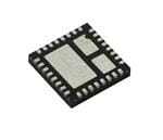
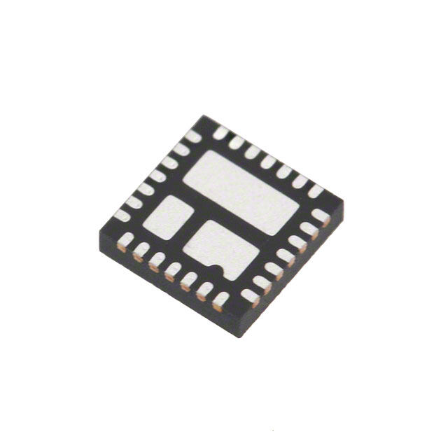
| 描述 | IC REG DL BCK/LINEAR SYNC 32MLPQ |
| 产品分类 | |
| 品牌 | Vishay Siliconix |
| 数据手册 | |
| 产品图片 |
|
| 产品型号 | SIC417CD-T1-E3 |
| rohs | 无铅 / 符合限制有害物质指令(RoHS)规范要求 |
| 产品系列 | microBUCK® |
| 产品培训模块 | http://www.digikey.cn/PTM/IndividualPTM.page?site=cn&lang=zhs&ptm=30381 |
| 供应商器件封装 | PowerPAK® MLP55-32 |
| 其它名称 | SIC417CD-T1-E3DKR |
| 功能 | 任何功能 |
| 包装 | Digi-Reel® |
| 安装类型 | 表面贴装 |
| 封装/外壳 | 32-PowerWFQFN |
| 工作温度 | -25°C ~ 125°C |
| 带LED驱动器 | 无 |
| 带定序器 | 无 |
| 带监控器 | 无 |
| 拓扑 | 降压(降压)同步(1),线性(LDO)(1) |
| 标准包装 | 1 |
| 特色产品 | http://www.digikey.cn/product-highlights/zh/microbuck-highlyintegrated-synchronous-buck-regulators/50410 |
| 电压-电源 | 3 V ~ 28 V |
| 电压/电流-输出1 | 0.5 V ~ 5.5 V,10A |
| 电压/电流-输出2 | 0.75 V ~ 5.25 V,150mA |
| 电压/电流-输出3 | - |
| 输出数 | 2 |
| 频率-开关 | 200kHz ~ 1MHz |


- 商务部:美国ITC正式对集成电路等产品启动337调查
- 曝三星4nm工艺存在良率问题 高通将骁龙8 Gen1或转产台积电
- 太阳诱电将投资9.5亿元在常州建新厂生产MLCC 预计2023年完工
- 英特尔发布欧洲新工厂建设计划 深化IDM 2.0 战略
- 台积电先进制程称霸业界 有大客户加持明年业绩稳了
- 达到5530亿美元!SIA预计今年全球半导体销售额将创下新高
- 英特尔拟将自动驾驶子公司Mobileye上市 估值或超500亿美元
- 三星加码芯片和SET,合并消费电子和移动部门,撤换高东真等 CEO
- 三星电子宣布重大人事变动 还合并消费电子和移动部门
- 海关总署:前11个月进口集成电路产品价值2.52万亿元 增长14.8%


PDF Datasheet 数据手册内容提取
SiC417 Vishay Siliconix microBUCKTM SiC417 10-A, 28-V Integrated Buck Regulator with Programmable LDO DESCRIPTION FEATURES The Vishay Siliconix SiC417 is an advanced stand-alone • High efficiency > 92 % synchronous buck regulator featuring integrated power (cid:129) Internal power MOSFETs: MOSFETs, bootstrap diode, and a programmable LDO in a High-side R = 27 mΩ DS(ON) space-saving MLPQ 5 x 5 - 32 pin package. Low-side R = 9 mΩ DS(ON) The SiC417 is capable of operating with all ceramic solutions (cid:129) Integrated bootstrap diode and switching frequencies up to 1 MHz. The programmable (cid:129) Integrated configurable 150 mA LDO with bypass logic frequency, synchronous operation and selectable (cid:129) Temperature compensated current limit power-save allow operation at high efficiency across the full range of load current. The internal programmable LDO may (cid:129) Pseudo fixed-frequency adaptive on-time control be used to supply 5 V for the gate drive circuits or it may be (cid:129) All ceramic solution enabled bypassed with an external 5 V for optimum efficiency and (cid:129) Programmable input UVLO threshold used to drive external N-channel MOSFETs or other loads. (cid:129) Independent enable pin for switcher and LDO Additional features include cycle-by-cycle current limit, voltage soft-start, under-voltage protection, programmable (cid:129) Selectable ultra-sonic power-save mode over-current protection, soft shutdown and selectable (cid:129) Internal soft-start and soft-shutdown power-save. The Vishay Siliconix SiC417 also provides an (cid:129) 1 % internal reference voltage enable input and a power good output. (cid:129) Power good output and over voltage protection • Halogen-free according to IEC 61249-2-21 definition (cid:129) Compliant to RoHS directive 2002/95/EC PRODUCT SUMMARY Input Voltage Range 3 V to 28 V APPLICATIONS Output Voltage Range 0.5 V to 5.5 V (cid:129) Notebook, desktop and server computers Operating Frequency 200 kHz to 1 MHz (cid:129) Digital HDTV and digital consumer applications Continuous Output Current 10 A (cid:129) Networking and telecommunication equipment Peak Efficiency 95 % at 300 kHz (cid:129) Printers, DSL and STB applications Package MLPQ 5 mm x 5 mm (cid:129) Embedded applications (cid:129) Point of load power supplies TYPICAL APPLICATION CIRCUIT 12 V5V DH VIN 3 6 VLDO BST 7 8 FBL 2 LX 13 EN/PSV PWM EN-PSAVE 29 Controller PGOOD PGOOD 26 27 ILIM ENL EN-LDO 32 15 31tON PGND5 AGND FB DL VOUT 30 1 14 Document Number: 69062 www.vishay.com S10-1367-Rev. D, 14-Jun-10 1
SiC417 Vishay Siliconix PIN CONFIGURATION V ENL tON AGND EN/PS LX ILIM PGOOD LX FB LX PAD 1 FBL LX V5V AGND 34 PGND AGND PAD 3 PGND VOUT LX 33 PGND VIN PAD 2 PGND VLDO VIN 35 PGND BST PGND N N N H X L D D VI VI VI D L D GN GN P P PIN DESCRIPTION Pin Number Symbol Description Feedback input for switching regulator. Connect to an external resistor divider from output to program the 1 FB output voltage. 2 FBL Feedback input for the LDO. Connect to an external resistor divider from V to program the V output. LDO LDO 5 V power input for internal analog circuits and gate drives. Connect to external 5 V supply or configure the 3 V5V LDO for 5 V and connect to V . LDO 4, 30, PAD 1 A Analog ground. GND 5 V Output voltage input to the SiC417. Additionally, may be used to bypass LDO to supply V directly. OUT LDO 6, 9 - 11, PAD 2 V Input supply voltage. IN 7 V LDO output. LDO Bootstrap pin. A capacitor is connected between BST to LX to develop the floating voltage for the high-side 8 BST gate drive. 12 DH High-side gate drive - do not connect this pin. 14 DL Low-side gate drive - do not connect this pin. 13, 23 - 25, 28, LX Switching (Phase) node. PAD 3 15-22 P Power ground. GND Open-drain power good indicator. High impedance indicates power is good. An external pull-up resistor is 26 P GOOD required. 27 I Current limit sense point - to program the current limit connect a resistor from I to LX. LIM LIM Tri-state pin. Enable input for switching regulator. Connect EN to A to disable the switching regulator. 29 EN/PSV GND Float pin for forced continuous and pull high for power-save mode. 31 t On-time set input. Set the on-time by a series resistor to the input supply voltage. ON 32 ENL Enable input for the LDO. Connect ENL to A to disable the LDO. GND ORDERING INFORMATION Part Number Package SiC417CD-T1-E3 MLPQ55-32 SiC417DB Evaluation board www.vishay.com Document Number: 69062 2 S10-1367-Rev. D, 14-Jun-10
SiC417 Vishay Siliconix FUNCTIONAL BLOCK DIAGRAM 3 26 29 6, 9 - 11 PAD 3 V5V V5V PGD EN/PSV VIN VIN AGND V5V BST 1.20.21 Reference Control and Status 8 PAD 1 DL Soft Start LX FB + Gate Drive 1238,, 2PA3 D- 235 Control V5V 1 - tON FB Comparator PGND 31 15-22 Zero Cross 5 VOUT Bypass Comparator Detector ILIM Valley 1 - Limit 27 VLDO VIN 7 Y BA LDO FBL MUX 2 ENL 32 ABSOLUTE MAXIMUM RATINGS T = 25 °C, unless otherwise noted A Parameter Symbol Min. Max. Unit LX to P Voltage V - 0.3 + 30 GND LX LX to P Voltage (transient - 100 ns) V - 2 + 30 GND LX V to P Voltage V - 0.3 + 30 IN GND IN V Maximum Voltage V - 0.3 V EN EN IN BST Bootstrap to LX; V5V to P - 0.3 + 6.0 V GND A to P V - 0.3 + 0.3 GND GND AG-PG EN/PSV, P , I , V , V , FB, FBL to GND - 0.3 + (V5V + 0.3) GOOD LIM OUT LDO t to P - 0.3 + (V5V - 1.5) ON GND BST to P - 0.3 + 35 GND Stresses beyond those listed under "Absolute Maximum Ratings" may cause permanent damage to the device. These are stress ratings only, and functional operation of the device at these or any other conditions beyond those indicated in the operational sections of the specifications is not implied. Exposure to absolute maximum rating/conditions for extended periods may affect device reliability. RECOMMENDED OPERATING CONDITIONS Parameter Symbol Min. Typ. Max. Unit Input Voltage V 3.0 28 IN V5V to P V5V 4.5 5.5 V GND V to P V 0.5 5.5 OUT GND OUT Note: For proper operation, the device should be used within the recommended conditions. THERMAL RESISTANCE RATINGS Parameter Symbol Min. Typ. Max. Unit Storage Temperature T - 40 + 150 STG Maximum Junction Temperature T - 150 °C J Operation Junction Temperature T - 25 + 125 J Document Number: 69062 www.vishay.com S10-1367-Rev. D, 14-Jun-10 3
SiC417 Vishay Siliconix THERMAL RESISTANCE RATINGS Thermal Resistance, Junction-to-Ambientb High-Side MOSFET 25 °C/W Low-Side MOSFET 20 PWM Controller and LDO Thermal Resistance 50 Peak IR Reflow Temperature T - 260 °C Reflow Notes: a. This device is ESD sensitive. Use of standard ESD handling precautions is required. b. Calculated from package in still air, mounted to 3 x 4.5 (in), 4 layer FR4 PCB with thermal vias under the exposed pad per JESD51 standards. Exceeding the above specifications may result in permanent damage to the device or device malfunction. Operation outside of the parameters specififed in the Electrical Characteristicsw section is not recommended. ELECTRICAL SPECIFICATIONS Test Conditions Unless Specified V = 12 V, V5V = 5 V, T = + 25 °C for typ., IN A - 25 °C to + 85 °C for min. and max., Parameter Symbol T = < 125 °C Min. Typ. Max. Unit J Input Supplies V Input Voltage V 3 28 IN IN V5V Voltage V5V 4.5 5.5 V Sensed at ENL pin, rising edge 2.4 2.6 2.95 V UVLO Threshold Voltagea IN_UV+ IN V Sensed at ENL pin, falling edge 2.235 2.4 2.565 IN_UV- V V UVLO Hysteresis V EN/PSV = High 0.2 IN IN_UV_HY V Measured at V5V pin, rising edge 3.7 3.9 4.1 V5V UVLO Threshold Voltage 5V_UV+ V Measured at V5V pin, falling edge 3.5 3.6 3.75 5V_UV- V5V UVLO Hysteresis V 0.3 5V_UV_HY EN/PSV, ENL = 0 V, V = 28 V 8.5 20 IN VIN Supply Current IIN Standby mode: 130 µA ENL = V5V, EN/PSV = 0 V EN/PSV, ENL = 0 V 3 7 EN/PSV = V5V, no load (f = 25 kHz), V5V Supply Current I SW 2 5V VFB > 500 mVb mA f = 250 kHz, EN/PSV = floating, no loadb 10 SW Controller F On-Time Threshold V Static V and load, - 40 °C to + 85 °C 0.495 0.5 0.505 V B FB-TH IN Frequency Range F continuous mode 200 1000 kHz PWM Bootstrap Switch Resistance 10 Ω Timing Continuous mode operation V = 15 V, On-Time t IN 999 1110 1220 ON V = 5 V, f = 300 kHz, R = 133 kΩ OUT SW ton ns Minimum On-Timeb t 50 ON Minimum Off-Timeb t 250 OFF Soft Start Soft Start Timeb t I = I /2 0.85 ms SS OUT LIM Analog Inputs/Outputs V Input Resistance R 500 kΩ OUT O-IN Current Sense Zero-Crossing Detector Threshold Voltage V LX-P - 3 0 + 3 mV Sense-th GND Power Good Power Good Threshold Voltage PG_V Internal reference 500 mV - 10 % + 20 % V TH Start-Up Delay Time PG_T V = 0 V 2 ms d EN Fault (noise-immunity) Delay Timeb PG_I V = 0 V 5 µs CC EN Power Good Leakage Current PG_I V = 0 V 1 µA LK EN Power Good On-Resistance PG_R V = 0 V 10 Ω DS-ON EN www.vishay.com Document Number: 69062 4 S10-1367-Rev. D, 14-Jun-10
SiC417 Vishay Siliconix ELECTRICAL SPECIFICATIONS Test Conditions Unless Specified V = 12 V, V5V = 5 V, T = + 25 °C for typ., IN A - 25 °C to + 85 °C for min. and max., Parameter Symbol T = < 125 °C Min. Typ. Max. Unit J Fault Protection I Source Current I 10 µA LIM LIM Valley Current Limit R = 5.9 kΩ 6 8 10 A ILIM I Comparator Offset Voltage V With respect to A - 10 0 + 10 mV LIM ILM-LK GND V with respect to Internal 500 mV reference, Output Under-Voltage Fault V FB - 25 % OUV_Fault 8 consecutive clocks Smart Power-Save Protection P V with respect to internal 500 mV reference + 10 Threshold Voltageb SAVE_VTH FB % Over-Voltage Protection Threshold V with respect to internal 500 mV reference + 20 FB Over-Voltage Fault Delayb t 5 µs OV-Delay Over Temperature Shutdownb T 10 °C hysteresis 150 °C Shut Logic Inputs/Outputs Logic Input High Voltage V 2 IN+ EN, ENL, PSV V Logic Input Low Voltage V 0.4 IN- EN/PSV Input Bias Current I EN/PSV = V5V or A - 10 + 10 EN- GND ENL Input Bias Current V = 28 V 11 18 µA IN FBL, FB Input Bias Current FBL_I FBL, FB = V5V or A - 1 + 1 LK GND Linear Dropout Regulator FBL Accuracy FBL V load = 10 mA 0.735 0.75 0.765 V ACC LDO Start-up and foldback, V = 12 V 85 LDO Current Limit LDO_I IN mA LIM Operating current limit, V = 12 V 135 200 IN V to V Switch-Over Thresholdc V - 140 + 140 LDO OUT LDO-BPS mV V to V Non-Switch-Over Thresholdc V - 450 + 450 LDO OUT LDO-NBPS V to V Switch-Over Resistance R V = 5 V 2 Ω LDO OUT LDO OUT From V to V , V = + 5 V, LDO Drop Out Voltaged IN VLDO VLDO 1.2 V I = 100 mA VLDO Notes: a.V is programmable using a resistor divider from V to ENL to A . The ENL voltage is compared to an internal reference. IN UVLO IN GND b.Guaranteed by design. c. The switch-over threshold is the maximum voltage diff erential between the V and V pins which ensures that V will internally LDO OUT LDO switch-over to V . The non-switch-over threshold is the minimum voltage diff erential between the V and V pins which ensures that OUT LDO OUT V will not switch-over to V . LDO OUT d.The LDO drop out voltage is the voltage at which the LDO output drops 2 % below the nominal regulation point. ELECTRICAL CHARACTERISTICS 100 95 VIN=9 V 90 85 VIN=19 V %) 80 y ( nc 75 e ci Effi 70 65 60 55 50 0 1 2 3 4 5 6 7 8 9 10 IOUT (A) Efficiency vs. Output Current (V = 1.2 V) OUT Document Number: 69062 www.vishay.com S10-1367-Rev. D, 14-Jun-10 5
SiC417 Vishay Siliconix ELECTRICAL CHARACTERISTICS 300 1.35 250 VIN=9 V VIN=19 V 1.3 z) 200 H quency (k 150 V (V)OUT 1.25 VIN=9 V VIN=19 V e Fr 100 1.2 50 0 1.15 0 1 2 3 4 5 6 7 8 9 10 0 1 2 3 4 5 6 7 8 9 10 IOUT (A) IOUT (A) Frequency vs. I , (V = 1.2 V) Load Regulation, (V = 1.2 V) OUT OUT OUT Start up Time: VIN = 12 V, VOUT = 1.2 V, IOUT = 0 A PGOOD Delay after Start up Time: V = 12 V, V = 1.2 V, I = 0 A IN OUT OUT Transient Response: VIN = 12 V, VOUT = 1.2 V, Transient Response: VIN = 12 V, VOUT = 1.2 V, IOUT = 10 A to 5 A, dI/dt = 0.5 A/µs IOUT = 5 A to 10 A, dI/dt = 0.5 A/µs www.vishay.com Document Number: 69062 6 S10-1367-Rev. D, 14-Jun-10
SiC417 Vishay Siliconix ELECTRICAL CHARACTERISTICS Over Current Protection: VIN = 12 V, VOUT = 1.2 V Ultra-Sonic Power-Save at IOUT = 0 A APPLICATIONS INFORMATION SiC417 Synchronous Buck Converter The SiC417 is a step down synchronous buck dc-to-dc VIN tON converter with integrated power FETs and programmable VLX LDO. The SiC417 is capable of 10 A operation at very high efficiency in a tiny 5 mm x 5 mm - 32 pin package. The CIN programmable operating frequency range of 200 kHz to Q1 VFB FB threshold 1 MHz, enables the user to optimize the solution for minimum board space and optimum efficiency. VLX VOUT The buck controller employs pseudo-fixed frequency L adaptive on-time control. This control scheme allows fast transient response thereby lowering the size of the power ESR Q2 components used in the system. FB + Input Voltage Range COUT The SiC417 requires two input supplies for normal operation: V and V5V. V operates over the wide range from 3 V to IN IN 28 V. V5V requires a 5 V supply input that can be an external source or the internal LDO configured to supply 5 V. When Figure 1 - Output Ripple and PWM Control Method V is less than ~ 6 V then an external 5 V supply must be IN tied to V5V. The adaptive on-time control has significant advantages over traditional control methods used in the controllers today. Pseudo-Fixed Frequency Adaptive On-Time Control (cid:129) Reduced component count by eliminating DCR sense or The PWM control method used for the SiC417 is current sense resistor as no need of a sensing inductor pseudo-fixed frequency, adaptive on-time, as shown in current. figure 1. The ripple voltage generated at the output capacitor (cid:129) Reduced Saves external components used for ESR is used as a PWM ramp signal. This ripple is used to compensation by eliminating the no error amplifier and trigger the on-time of the controller. other components. The adaptive on-time is determined by an internal oneshot (cid:129) Ultra fast transient response because of fast loop, timer. When the one-shot is triggered by the output ripple, the absence of error amplifier speeds up the transient device sends a single on-time pulse to the highside response. MOSFET. The pulse period is determined by VOUT and VIN; (cid:129) Predictable frequency spread because of constant on-time the period is proportional to output voltage and inversely architecture. proportional to input voltage. With this adaptive on-time (cid:129) Fast transient response enables operation with minimum arrangement, the device automatically anticipates the output capacitance on-time needed to regulate VOUT for the present VIN Overall, superior performance compared to fixed frequency condition and at the selected frequency. architectures. Document Number: 69062 www.vishay.com S10-1367-Rev. D, 14-Jun-10 7
SiC417 Vishay Siliconix On-Time One-Shot Generator (t ) and Operating ON Frequency VOUT To FB pin The SiC417 have an internal on-time one-shot generator R1 which is a comparator that has two inputs. The FB Comparator output goes high when VFB is less than the R2 internal 500 mV reference. This feeds into the gate drive and turns on the high-side MOSFET, and also starts the one-shot timer. The one-shot timer uses an internal comparator and a capacitor. One comparator input is connected to V , the OUT other input is connected to the capacitor. When the on-time Figure 3 - Output Voltage Selection begins, the internal capacitor charges from zero volts through a current which is proportional to V . When the As the control method regulates the valley of the output ripple IN capacitor voltage reaches VOUT, the on-time is completed voltage, the DC output voltage VOUT is off set by the output and the high-side MOSFET turns off. The figure 2 shows the ripple according to the following equation. on-chip implementation of on-time generation. V = 0.5 x (1 + R /R ) + V /2 OUT 1 2 RIPPLE Gate FB comparator drives Enable and Power-Save Inputs FB - 500 mV + The EN/PSV and ENL inputs are used to enable or disable QQ11 DH VLX L VOUT the switching regulator and the LDO. When EN/PSV is low (grounded), the switching regulator is VOUT ESR FB off and in its lowest power state. When off, the output of the VIN Ontiem-sehrot DL Q2 COUT + switching regulator soft-discharges the output into a 15 Ω internal resistor via the V pin. OUT Rton On-time = K x Rton x (VOUT/VIN) When EN/PSV is allowed to float, the pin voltage will fl oat to 1.5 V. The switching regulator turns on with power-save Figure 2 - On-Time Generation disabled and all switching is in forced continuous mode. When EN/PSV is high (above 2.0 V), the switching regulator This method automatically produces an on-time that is turns on with ultra-sonic power-save enabled. The SiC417 proportional to V and inversely proportional to V . Under ultra-sonic power-save operation maintains a minimum OUT IN steady-state conditions, the switching frequency can be switching frequency of 25 kHz, for applications with stringent determined from the on-time by the following equation. audio requirements. The ENL input is used to control the internal LDO. This input fSW = VOUT serves a second function by acting as a VIN UVLO sensor for tON x VIN the switching regulator. The LDO is off when ENL is low (grounded). When ENL is a The SiC417 uses an external resistor to set the ontime which logic high but below the V threshold (2.6 V typical), IN UVLO indirectly sets the frequency. The on-time can be then the LDO is on and the switcher is off. When ENL is programmed to provide operating frequency from 200 kHz to above the V threshold, the LDO is enabled and the IN UVLO 1 MHz using a resistor between the t pin and ground. The ON switcher is also enabled if the EN/PSV pin is not grounded. resistor value is selected by the following equation. Forced Continuous Mode Operation Rton =(tON - 10 ns) x VIN The SiC417 operates the switcher in Forced Continuous 25 pF x VOUT Mode (FCM) by floating the EN/PSV pin (see figure 4). In this The maximum R value allowed is shown by the following mode one of the power MOSFETs is always on, with no TON equation. intentional dead time other than to avoid cross-conduction. This feature results in uniform frequency across the full load Rton_MAX = VIN_MIN range with the trade-off being poor efficiency at light loads 15 µA due to the high-frequency switching of the MOSFETs. V Voltage Selection OUT The switcher output voltage is regulated by comparing V OUT as seen through a resistor divider at the FB pin to the internal 500 mV reference voltage, see figure 3. www.vishay.com Document Number: 69062 8 S10-1367-Rev. D, 14-Jun-10
SiC417 Vishay Siliconix Because the on-times are forced to occur at intervals no FB ripple greater than 40 µs, the frequency will not fall below ~ 25 kHz. voltage (VFB) FB threshold (500 mV) Figure 5 shows ultra-sonic power-save operation. Benefits of Ultrasonic Power-Save Inductor DC load current Having a fixed minimum frequency in power-save has some current significant advantages as below: (cid:129) The minimum frequency of 25 kHz is outside the audible range of human ear. This makes the operation of the SiC417 very quiet. On-time DH on-time is triggered when (cid:129) The output voltage ripple seen in power-save mode is (tON) VFB reaches the FB threshold significant lower than conventional power-save, which improves efficiency at light loads. DH (cid:129) Lower ripple in power-save also makes the power component selection easier. DL DL drives high when on-time is completed. DL remains high until VFB falls to the FB threshold. Figure 4 - Forced Continuous Mode Operation Ultrasonic Power-Save Operation The SiC417 provides ultra-sonic power-save operation at light loads, with the minimum operating frequency fixed at 25 kHz. This is accomplished using an internal timer that monitors the time between consecutive high-side gate pulses. If the time exceeds 40 µs, DL drives high to turn the low-side MOSFET on. This draws current from V through the OUT inductor, forcing both V and V to fall. When V drops OUT FB FB to the 500 mV threshold, the next DH on-time is triggered. After the on-time is completed the high-side MOSFET is turned off and the low-side MOSFET turns on, the low-side Figure 6 - Ultrasonic Power-Save Operation Mode MOSFET remains on until the inductor current ramps down to zero, at which point the low-side MOSFET is turned off. Figure 6 shows the behavior under power-save and continuous conduction mode at light loads. minimum fSW ~ 25 kHz Smart Power-Save Protection FB ripple Active loads may leak current from a higher voltage into the voltage (VFB) switcher output. Under light load conditions with power- FB threshold (500 mV) savepower-save enabled, this can force VOUT to slowly rise and reach the over-voltage threshold, resulting in a hard Inductor (0A) shutdown. Smart power-save prevents this condition. current When the FB voltage exceeds 10 % above nominal (exceeds 550 mV), the device immediately disables power-save, and DL drives high to turn on the low-side MOSFET. This draws DH on-time is triggered when On-time current from V through the inductor and causes V to (tON) VFB reaches the FB threshold fall. When V O dUroTps back to the 500 mV trip point, a nOoUrTmal FB DH tON switching cycle begins. This method prevents a hard OVP shutdown and also cycles energy from V back to V . It also minimizes operating OUT IN power by avoiding forced conduction mode operation. DL Figure 7 shows typical waveforms for the smart power-save feature. After the 40 µs time-out, DL drives high if VFB has not reached the FB threshold. Figure 5 - Ultrasonic power-save Operation Document Number: 69062 www.vishay.com S10-1367-Rev. D, 14-Jun-10 9
SiC417 Vishay Siliconix Note that because the low-side MOSFET with low RDS(ON) is VOUT drifts up to due to leakage used for current sensing, the PCB layout, solder current flowing into COUT VOUT discharges via inductor connections, and PCB connection to the LX node must be Smart power save and low-side MOSFET threshold (550 mV) done carefully to obtain good results. Refer to the layout Normal VOUT ripple FB guidelines for information. threshold DH and DL off Soft-Start of PWM Regulator Soft-start is achieved in the PWM regulator by using an High-side drive (DH) internal voltage ramp as the reference for the FB Single DH on-time pulse Comparator. The voltage ramp is generated using an internal after DL turn-off charge pump which drives the reference from zero to 500 mV in ~ 1.2 mV increments, using an internal ~ 500 kHz Low-side oscillator. When the ramp voltage reaches 500 mV, the ramp drive (DL) is ignored and the FB comparator switches over to a fixed DL turns on when smart Normal DL pulse after DH PSAVE threshold is reached on-time pulse 500 mV threshold. During soft-start the output voltage tracks DL turns off FB the internal ramp, which limits the start-up inrush current and threshold is reached provides a controlled softstart profile for a wide range of Figure 7 - Smart Power-Save applications. Typical softstart ramp time is 850 µs. During soft-start the regulator turns off the low-side MOSFET on any Current Limit Protection cycle if the inductor current falls to zero. This prevents The SiC417 features programmable current limit capability, negative inductor current, allowing the device to start into a which is accomplished by using the R of the lower DS(ON) pre-biased output. MOSFET for current sensing. The current limit is set by R ILIM resistor. The R resistor connects from the I pin to the ILIM LIM Power Good Output LX pin which is also the drain of the low-side MOSFET. The power good (P ) output is an open-drain output GOOD When the low-side MOSFET is on, an internal ~ 10 µA which requires a pull-up resistor. When the output voltage is current flows from the I pin and the R resistor, creating LIM ILIM 10 % below the nominal voltage, P is pulled low. It is GOOD a voltage drop across the resistor. While the low-side held low until the output voltage returns above - 8 % of MOSFET is on, the inductor current flows through it and nominal. P is held low during start-up and will not be GOOD creates a voltage across the R . The voltage across the DS(ON) allowed to transition high until soft-start is completed (when MOSFET is negative with respect to ground. V reaches 500 mV) and typically 2 ms has passed. FB If this MOSFET voltage drop exceeds the voltage across P will transition low if the V pin exceeds + 20 % of GOOD FB R , the voltage at the I pin will be negative and current ILIM LIM nominal, which is also the over-voltage shutdown threshold limit will activate. The current limit then keeps the low-side (600 mV). P also pulls low if the EN/PSV pin is low GOOD MOSFET on and will not allow another high-side on-time, when V5V is present. until the current in the low-side MOSFET reduces enough to bring the I voltage back up to zero. This method regulates LIM Output Over-Voltage Protection the inductor valley current at the level shown by I in LIM Over-voltage protection becomes active as soon as the figure 8. device is enabled. The threshold is set at 500 mV + 20 % (600 mV). When V exceeds the OVP threshold, DL latches FB IPEAK high and the low-side MOSFET is turned on. DL remains urrent ILOAD htoigghg laendd o trh Ve5 cVo nistr ocylleclre rde.m Tahienrse o ifsf ,a u 5n tµil st hdee ElaNy /bPuSilVt iinntpou tth ies C or ILIM OVP detector to prevent false transitions. PGOOD is also low uct after an OVP event. d n I Output Under-Voltage Protection Time When VFB falls 25 % below its nominal voltage (falls to Figure 8 - Valley Current Limit 375 mV) for eight consecutive clock cycles, the switcher is shut off and the DH and DL drives are pulled low to tristate Setting the valley current limit to 10 A results in a 10 A peak the MOSFETs. The controller stays off until EN/PSV is inductor current plus peak ripple current. In this situation, the toggled or V5V is cycled. average (load) current through the inductor is 10 A plus one-half the peak-to-peak ripple current. V5V UVLO, and POR The internal 10 µA current source is temperature Under-voltage lock-out (UVLO) circuitry inhibits switching compensated at 4100 ppm in order to provide tracking with and tri-states the DH/DL drivers until V5V rises above 3.9 V. the R . The R value is calculated by the following An internal Power-On Reset (POR) occurs when V5V DS(ON) ILIM equation. exceeds 3.9 V, which resets the fault latch and soft-start R = 735 x I ILIM LIM www.vishay.com Document Number: 69062 10 S10-1367-Rev. D, 14-Jun-10
SiC417 Vishay Siliconix counter to prepare for soft-start. The SiC417 then begins a LDO Switchover Function soft-start cycle. The PWM will shut off if V5V falls below The SiC417 includes a switch-over function for the LDO. The 3.6 V. switch-over function is designed to increase efficiency by using the more efficient dc-to-dc converter to power the LDO LDO Regulator output, avoiding the less efficient LDO regulator when The SiC417 features an integrated LDO regulator with a possible. The switch-over function connects the V pin LDO programmable output voltage from 0.75 V to 5.25 V using directly to the V pin using an internal switch. When the OUT external resistors, when an external supply is used to power switch-over is complete the LDO is turned off, which results V5V. The feedback pin (FBL) for the LDO is regulated to 750 in a power savings and maximizes efficiency. If the LDO mV. There is also an enable pin (ENL) for the LDO that output is used to bias the SiC417, then after switch-over the provides independent control. The LDO voltage can also be device is self-powered from the switching regulator with the used to provide the bias voltage for the switching regulator, LDO turned off. when V is tied to V5V. More detail can be found in the On The switch-over logic waits for 32 switching cycles before it LDO Chip LDO bias section coming up. starts the switch-over. There are two methods that determine the switch-over of V to V . LDO OUT VLDO To FBL pin In the first method, the LDO is already in regulation and the RLDO1 dc-to-dc converter is later enabled. As soon as the PGOOD output goes high, the 32 cycles are started. The voltages at RLDO2 the VLDO and VOUT pins are then compared; if the two voltages are within ± 300 mV of each other, the V pin LDO connects to the V pin using an internal switch, and the OUT LDO is turned off. In the second method, the dc-to-dc converter is already Figure 9 - LDO Start-Up running and the LDO is enabled. In this case the 32 cycles are started as soon as the LDO reaches 90 % of its final The LDO output voltage is set by the following equation. value. At this time, the V and V pins are compared, LDO OUT and if within ± 300 mV the switch-over occurs and the LDO VLDO = 750 mV x 1+(RLDO1) is turned off. RLDO2 Benefits of having a switchover circuit A minimum capacitance of 1 µF referenced to AGND is The switchover function is designed to get maximum normally required at the output of the LDO for stability. If the efficiency out of the dc-to-dc converter. The efficiency for an LDO is providing bias power to the device, then a minimum LDO is very low especially for high input voltages. Using the 0.1 µF capacitor referenced to A is required along with a GND switchover function we tie any rails connected to V minimum 1.0 µF capacitor referenced to P to filter the LDO GND through a switch directly to V . Once switchover is gate drive pulses. Refer to the layout guideline section. OUT complete LDO is turned off which saves power. This gives us the maximum efficiency out of the SiC417. LDO Start-up If the LDO output is used to bias the SiC417, then after Before start-up, the LDO checks the status of the following switchover the V self biases the SiC417 and operates in signals to ensure proper operation can be maintained. OUT self-powered mode. 1. ENL pin Steps to follow when using the on chip LDO to bias the 2. V output LDO SiC417: 3. V input voltage IN (cid:129) Always tie the V5V to V before enabling the LDO When the ENL pin is high and V is above the UVLO point, LDO IN (cid:129) Enable the LDO before enabling the switcher the LDO will begin start-up. During the initial phase, when the (cid:129) LDO has a current limit of 85 mA at start-up with 12 V , so LDO output voltage is near zero, the LDO initiates a IN do not connect any load between V and ground current-limited start-up (typically 85 mA) to charge the output LDO (cid:129) The current limit for the LDO goes up to 200 mA once the capacitor. When V has reached 90 % of the final value LDO V reaches 90 % of its final values and can easily supply (as sensed at the FBL pin), the LDO current limit is increased LDO the required bias current to the IC. to ~ 200 mA and the LDO output is quickly driven to the nominal value by the internal LDO regulator. Switch-over Limitations on V and V OUT LDO Because the internal switch-over circuit always compares VVLDO final the V and V pins at start-up, there are limitations on Voltage regulating with OUT LDO permissible combinations of V and V . Consider the ~ 200 mA current limit OUT LDO 90 % of VVLDO final case where V is programmed to 1.5 V and V is OUT LDO programmed to 1.8 V. After start-up, the device would connect V to V and disable the LDO, since the two Constant current startup OUT LDO voltages are within the ± 300 mV switch-over window. Figure 10 - LDO Start-Up Document Number: 69062 www.vishay.com S10-1367-Rev. D, 14-Jun-10 11
SiC417 Vishay Siliconix To avoid unwanted switch-over, the minimum difference However, if the switcher was previously operating (with EN/ between the voltages for V and V should be PSV high but ENL at ground, and V5V supplied externally), OUT LDO ± 500 mV. then it is undesirable to shut down the switcher. It is not recommended to use the switch-over feature for an To prevent this, when the ENL input is taken above 2.6 V output voltage less than 3 V since this does not provide (above the V UVLO threshold), the internal logic checks the IN sufficient voltage for the gate-source drive to the internal P signal. If P is high, then the switcher is already GOOD GOOD p-channel switch-over MOSFET. running and the LDO will run through the start-up cycle without affecting the switcher. If P is low, then the LDO GOOD Switch-Over MOSFET Parasitic Diodes will not allow any PWM switching until the LDO output has The switch-over MOSFET contains parasitic diodes that are reached 90 % of it's final value. inherent to its construction, as shown in figure 11. On-Chip LDO Bias the SiC417 Switchover control Switchover The following steps must be followed when using the onchip MOSFET LDO to bias the device. VLDO VOUT (cid:129) Connect V5V to VLDO before enabling the LDO. (cid:129) The LDO has an initial current limit of 85 mA at start-up with 12 V , therefore, do not connect any external load to IN V during start-up. LDO (cid:129) When V reaches 90 % of its final value, the LDO LDO current limit increases to 200 mA. At this time the LDO may Parastic diode Parastic diode be used to supply the required bias current to the device. V5V (cid:129) Switching will be held off until V reaches regulation. LDO Figure 11 - Switch-over MOSFET Parasitic Diodes Attempting to operate in self-powered mode in any other configuration can cause unpredictable results and may There are some important design rules that must be followed damage the device. to prevent forward bias of these diodes. The following two conditions need to be satisfied in order for the parasitic Design Procedure diodes to stay off. When designing a switch mode power supply, the input (cid:129) V5V ≥ VLDO voltage range, load current, switching frequency, and (cid:129) V5V ≥ VOUT inductor ripple current must be specified. If either VLDO or VOUT is higher than V5V, then the respective The maximum input voltage (VINMAX) is the highest specified diode will turn on and the SiC417 operating current will flow input voltage. The minimum input voltage (V ) is INMIN through this diode. This has the potential of damaging the determined by the lowest input voltage after evaluating the device. voltage drops due to connectors, fuses, switches, and PCB traces. ENL Pin and VIN UVLO The following parameters define the design: The ENL pin also acts as the switcher under-voltage lockout (cid:129) Nominal output voltage (V ) OUT for the VIN supply. The VIN UVLO voltage is programmable (cid:129) Static or DC output tolerance via a resistor divider at the VIN, ENL and AGND pins. (cid:129) Transient response ENL is the enable/disable signal for the LDO. In order to (cid:129) Maximum load current (I ) OUT implement the VIN UVLO there is also a timing requirement There are two values of load current to evaluate - continuous that needs to be satisfied. load current and peak load current. Continuous load current If the ENL pin transitions low within 2 switching cycles and is relates to thermal stresses which drive the selection of the < 1 V, then the LDO will turn off but the switcher remains on. inductor and input capacitors. Peak load current determines If ENL goes below the VIN UVLO threshold and stays above instantaneous component stresses and filtering 1 V, then the switcher will turn off but the LDO remains on. requirements such as inductor saturation, output capacitors, The VIN UVLO function has a typical threshold of 2.6 V on the and design of the current limit circuit. VIN rising edge. The falling edge threshold is 2.4 V. The following values are used in this design: Note that it is possible to operate the switcher with the LDO (cid:129) V = 12 V ± 10 % IN disabled, but the ENL pin must be below the logic low (cid:129) V = 1.05 V ± 4 % OUT threshold (0.4 V maximum). (cid:129) f = 250 kHz SW (cid:129) Load = 10 A maximum ENL Logic Control of PWM Operation When the ENL input is driven above 2.6 V, it is impossible to determine if the LDO output is going to be used to power the device or not. In self-powered operation where the LDO will power the device, it is necessary during the LDO start-up to hold the PWM switching off until the LDO has reached 90 % of the final value. This is to prevent overloading the current-limited LDO output during the LDO start-up. www.vishay.com Document Number: 69062 12 S10-1367-Rev. D, 14-Jun-10
SiC417 Vishay Siliconix Frequency Selection Note that the inductor must be rated for the maximum DC Selection of the switching frequency requires making a load current plus 1/2 of the ripple current. The ripple current trade-off between the size and cost of the external filter under minimum V conditions is also checked using the IN components (inductor and output capacitor) and the power following equations. conversion efficiency. The desired switching frequency is 250 kHz which results TON_VINMIN =25 pF x RTON x VOUT from using component selected for optimum size and cost. VINMIN A resistor (R ) is used to program the on-time (indirectly setting the freTqOuNency) using the following equation. IRIPPLE = (VIN - VOUT) x TON L Rton =(tON2 5- 1p0F nx sV) OxU VTIN IRIPPLE_VIN =(10.8 - 01..8085 )µ xH 384 ns = 4.25 A To select R , use the maximum value for V , and for t Capacitor Selection TON IN ON use the value associated with maximum V . The output capacitors are chosen based on required ESR IN and capacitance. The maximum ESR requirement is tON = VOUT controlled by the output ripple requirement and the DC VINMAX. x fSW tolerance. The output voltage has a DC value that is equal to the valley of the output ripple plus 1/2 of the peak-to-peak t = 318 ns at 13.2 V , 1.05 V , 250 kHz ON IN OUT ripple. Change in the output ripple voltage will lead to a Substituting for R results in the following solution TON change in DC voltage at the output. R = 154.9 kΩ, use R = 154 kΩ. TON TON The design goal is that the output voltage regulation be ± 4 % under static conditions. The internal 500 mV reference Inductor Selection tolerance is 1 %. Allowing 1 % tolerance from the FB resistor In order to determine the inductance, the ripple current must divider, this allows 2 % tolerance due to V ripple. first be defined. Low inductor values result in smaller size but OUT Since this 2 % error comes from 1/2 of the ripple voltage, the create higher ripple current which can reduce efficiency. allowable ripple is 4 %, or 42 mV for a 1.05 V output. Higher inductor values will reduce the ripple current and The maximum ripple current of 4.4 A creates a ripple voltage voltage and for a given DC resistance are more efficient. across the ESR. The maximum ESR value allowed is shown However, larger inductance translates directly into larger by the following equations. packages and higher cost. Cost, size, output ripple, and efficiency are all used in the selection process. VRIPPLE 42 mV The ripple current will also set the boundary for power-save ESRMAX = = IRIPPLEMAX 4.4 A operation. The switching will typically enter power-save mode when the load current decreases to 1/2 of the ripple ESRMAX = 9.5 mΩ current. For example, if ripple current is 4 A then power-save operation will typically start for loads less than 2 A. If ripple The output capacitance is usually chosen to meet transient current is set at 40 % of maximum load current, then power- requirements. A worst-case load release, from maximum save will start for loads less than 20 % of maximum current. load to no load at the exact moment when inductor current is The inductor value is typically selected to provide a ripple at the peak, determines the required capacitance. If the load current that is between 25 % to 50 % of the maximum load release is instantaneous (load changes from maximum to current. This provides an optimal trade-off between cost, zero in < 1 µs), the output capacitor must absorb all the efficiency, and transient performance. inductor's stored energy. This will cause a peak voltage on During the DH on-time, voltage across the inductor is the capacitor according to the following equation. (V -V ). The equation for determining inductance is IN OUT shown next. L (IOUT + 12 x IRIPPLEMAX)2 COUTMIN = L =(VIN - VOUT) x tON (VPEAK)2 - (VOUT)2 IRIPPLE Assuming a peak voltage V of 1.150 (100 mV rise upon PEAK Example load release), and a 10 A load release, the required In this example, the inductor ripple current is set equal to capacitance is shown by the next equation. 50 % of the maximum load current. Thus ripple current will be 50 % x 10 A or 5 A. To find the minimum inductance needed, 1 0.88 µH (10 + x 4.4)2 use the VIN and TON values that correspond to VINMAX. COUTMIN = 2 (1.15)2 - (1.05)2 (13.2 - 1.05) x 318 ns L = 5 A = 77 µH COUTMIN = 595 µF If the load release is relatively slow, the output capacitance A slightly larger value of 0.88 µH is selected. This will can be reduced. At heavy loads during normal switching, decrease the maximum I to 4.4 A. RIPPLE when the FB pin is above the 500 mV reference, the DL Document Number: 69062 www.vishay.com S10-1367-Rev. D, 14-Jun-10 13
SiC417 Vishay Siliconix output is high and the low-side MOSFET is on. During this time, the voltage across the inductor is approximately - V . CTOP OUT This causes a down-slope or falling di/dt in the inductor. If the load dI/dt is not much faster than the - dI/dt in the inductor, then the inductor current will tend to track the falling load current. This will reduce the excess inductive energy that must be absorbed by the output capacitor, therefore a VOUT R1 To FB pin smaller capacitance can be used. The following can be used to calculate the needed R2 capacitance for a given dI /dt: LOAD Peak inductor current is shown by the next equation. ILPK = IMAX + 1/2 x IRIPPLEMAX I = 10 + 1/2 x 4.4 = 12.2 A LPK Rate of change of load current = dI /dt Figure 13 - Capacitor Coupling to FB Pin LOAD I = maximum load release = 10 A MAX Another way to eliminate doubling-pulsing is to add a small L x I L P K - I M A X x dt (~ 10 pF) capacitor across the upper feedback resistor, as COUT = ILPK x VOUT dlLOAD shown in figure 13. This capacitor should be left unpopulated 2 (VPK - VOUT) until it can be confirmed that double-pulsing exists. Adding Example the CTOP capacitor will couple more ripple into FB to help eliminate the problem. An optional connection on the PCB Load dlLOAD =2.5 A should be available for this capacitor. dt µs ESR loop instability is caused by insufficient ESR. The details of this stability issue are discussed in the ESR This would cause the output current to move from 10 A to Requirements section. The best method for checking zero in 4 µs as shown by the following equation. stability is to apply a zero-to-full load transient and observe the output voltage ripple envelope for overshoot and ringing. 12.2 10 0.88 µH x 1 . 0 5 - 2 . 5 x 1 µs Ringing for more than one cycle after the initial step is an COUT = 12.2 x 2 (1.15 - 1.05) indication that the ESR should be increased. One simple way to solve this problem is to add trace COUT = 379 µF resistance in the high current output path. A side effect of Note that C is much smaller in this example, 379 µF adding trace resistance is output decreased load regulation. OUT compared to 595 µF based on a worst-case load release. To meet the two design criteria of minimum 379 µF and ESR Requirements maximum 9 mΩ ESR, select two capacitors rated at 220 µF A minimum ESR is required for two reasons. One reason is and 15 mΩ ESR. to generate enough output ripple voltage to provide10 mVp-p It is recommended that an additional small capacitor be at the FB pin (after the resistor divider) to avoid double- placed in parallel with C in order to filter high frequency pulsing. OUT switching noise. The second reason is to prevent instability due to insufficient ESR. The on-time control regulates the valley of the output Stability Considerations ripple voltage. This ripple voltage is the sum of the two Unstable operation is possible with adaptive on-time voltages. One is the ripple generated by the ESR, the other controllers, and usually takes the form of double-pulsing or is the ripple due to capacitive charging and discharging ESR loop instability. during the switching cycle. For most applications the Double-pulsing occurs due to switching noise seen at the FB minimum ESR ripple voltage is dominated by the output input or because the FB ripple voltage is too low. This causes capacitors, typically SP or POSCAP devices. For stability the the FB comparator to trigger prematurely after the 250 ns ESR zero of the output capacitor should be lower than minimum off-time has expired. In extreme cases the noise approximately one-third the switching frequency. The can cause three or more successive on-times. formula for minimum ESR is shown by the following Double-pulsing will result in higher ripple voltage at the equation. output, but in most applications it will not affect operation. 3 This form of instability can usually be avoided by providing ESRMIN = the FB pin with a smooth, clean ripple signal that is at least 2 x π x COUT x fSW 10 mV , which may dictate the need to increase the ESR of p-p For applications using ceramic output capacitors, the ESR is the output capacitors. It is also imperative to provide a proper normally too small to meet the above ESR criteria. In these PCB layout as discussed in the Layout Guidelines section. applications it is necessary to add a small virtual ESR network composed of two capacitors and one resistor, as shown in figure 14. This network creates a ramp voltage www.vishay.com Document Number: 69062 14 S10-1367-Rev. D, 14-Jun-10
SiC417 Vishay Siliconix across C , analogous to the ramp voltage generated across This trace resistance should be optimized so that at full load L the ESR of a standard capacitor. This ramp is then the output droops to near the lower regulation limit. Passive capacitive-coupled into the FB pin via capacitor C . droop minimizes the required output capacitance because C the voltage excursions due to load steps are reduced as seen at the load. L The use of 1 % feedback resistors contributes up to 1 % error. If tighter DC accuracy is required, 0.1 % resistors High- side should be used. RL CL The output inductor value may change with current. This will change the output ripple and therefore will have a minor R1 effect on the DC output voltage. The output ESR also affects CC the output ripple and thus has a minor effect on the DC Low- COUT output voltage. side R2 Switching Frequency Variations FB The switching frequency will vary depending on line and load pin conditions. The line variations are a result of fixed propagation delays in the on-time one-shot, as well as unavoidable delays in the external MOSFET switching. As Figure 14 - Virtual ESR Ramp Current V increases, these factors make the actual DH on-time IN slightly longer than the ideal on-time. The net effect is that Dropout Performance frequency tends to falls slightly with increasing input voltage. The output voltage adjusts range for continuous-conduction The switching frequency also varies with load current as a operation is limited by the fixed 250 ns (typical) minimum result of the power losses in the MOSFETs and the inductor. off-time of the one-shot. When working with low input For a conventional PWM constant-frequency converter, as voltages, the duty-factor limit must be calculated using load increases the duty cycle also increases slightly to worst-case values for on and off times. The duty-factor compensate for IR and switching losses in the MOSFETs limitation is shown by the next equation. and inductor. A constant on-time converter must also compensate for the TON(MIN) same losses by increasing the effective duty cycle (more DUTY = TON(MIN) x TOFF(MAX) time is spent drawing energy from VIN as losses increase). The on-time is essentially constant for a given V /V OUT IN The inductor resistance and MOSFET on-state voltage drops combination, to off set the losses the off-time will tend to must be included when performing worst-case dropout reduce slightly as load increases. The net effect is that duty-factor calculations. switching frequency increases slightly with increasing load. System DC Accuracy (V Controller) OUT Three factors affect V accuracy: the trip point of the FB OUT error comparator, the ripple voltage variation with line and load, and the external resistor tolerance. The error comparator off set is trimmed so that under static conditions it trips when the feedback pin is 500 mV, 1 %. The on-time pulse from the SiC417 in the design example is calculated to give a pseudo-fixed frequency of 250 kHz. Some frequency variation with line and load is expected. This variation changes the output ripple voltage. Because constant on-time converters regulate to the valley of the output ripple, ½ of the output ripple appears as a DC regulation error. For example, if the output ripple is 50 mV with V = 6 V, then the measured DC output will be 25 mV IN above the comparator trip point. If the ripple increases to 80 mV with V = 25 V, then the measured DC output will be IN 40 mV above the comparator trip. The best way to minimize this effect is to minimize the output ripple. To compensate for valley regulation, it may be desirable to use passive droop. Take the feedback directly from the output side of the inductor and place a small amount of trace resistance between the inductor and output capacitor. Document Number: 69062 www.vishay.com S10-1367-Rev. D, 14-Jun-10 15
SiC417 Vishay Siliconix SiC417 EVALUATION BOARD SCHEMATIC VOB3 1 1 B4B4 VO_GND P9 VCTRL P11VO_GND 1 1 C422 µF P10VoVO 1 1 J6J6Probe Test PinProbe Test Pin34 C322 µF R10R1010K10K R23R237.15K7.15K 5 2 C222 µF R5C1100K22 µF C7C70.1 µF C23C17220 µF220 µF ++++ C2568 pF C31100 pF * Q1Si4812BDY C18C16220 µF220 µF ++++ 1 Step_I_Sense R41R01 1P12LDTRG C20C15C22C2110 µF 10 µF10 µF10 µF PGOOD V5V P8 R31K J55Probe Test Pin L11 µH C191µ * R9C14*0.1 µF C2410n * R131K P7P71 J2J1J1Probe Test PinProbe Test PinProbe Test Pin33141422V5V55 R1300K *P5P5234J351Probe Test Pin P6EN_PSV1R21300K * ENLC50.1 µF234 R6100K3VR7IN0J41C6Probe Test Pin24925811230.1 µFVLTHLTUNDS336SDOEVBLXP9VIN/NV1028INEVLX2511C9C11C13C10INVLX342410 µF0.1 µF0.01 µF10 µFINVLX23R8R40INLXΩ13U1U11 10KLX3SiC417SiC417V5V727VILIMLDO1FBR110C28R12DDDDDDDDDDD22657.6K0.1 µFNNNNNNNNNNNFBLPGD31C30GGGGGGGGGGGTONAPPPPPPPPAA47 pF562109870541122213113 R29C2922 µF10KC321n1 R1510KR390RR30P475KVLDO M4M3M2 111111 24 5 1 C810 µF C274.7 µF * P1VIN 11 ++C12150 µF C264.7 µF J71Probe Test Pin5 24 M1 11 3 P2VIN_GND B11VIN 1B2VIN_GND V5V 1 P3P3V5VV5V Figure 15. Evaluation Board Schematic www.vishay.com Document Number: 69062 16 S10-1367-Rev. D, 14-Jun-10
SiC417 Vishay Siliconix BILL OF MATERIALS Reference Designator Value Voltage Footprint Part Number Manufacturer B1, B2, B3, B4 SOLDER-BANANA 575-4 Keystone C29 22 µF 16 V SM/C_1210 GRM32ER71C226ME18L Murata C5 0.1 µF 10 V SM/C_0402 C0402C104K8RAC7867 Vishay C6 0.1 µF 10 V SM/C_0805 C0402C104K8RAC7867 Vishay C11, C14, C28 0.1 µF 50 V SM/C_0603 VJ0603Y104KXACW1BC Vishay C8, C9, C10 10 µF 25 V SM/C_1210 TMK325B7106MN-T Taiyo Yuden C12 150 µF 35 V D8X11.5-D0.6X3.5 EEU-FM1V151 Panasonic C13 0.01 µF 50 V SM/C_0402 VJ0402Y103KXACW1BC Vishay C15, C20, C21, C22 10 µF 16 V SM/C_1206 GRM31CR71C106KAC7L C16, C17, C18, C23 220 µF 10 V 595D-D 593D227X0010E2TE3 Vishay C19 1 µF SM/C_0603 C24 10 nF SM/C_0603 C25 100 pF 50 V SM/C_0402 VJ0402A101JXACW1BC Vishay C26 4.7 µF 10 V SM/C_0805 LMK212B7475KG-T Taiyo Yuden C27 4.7 µF 10 V SM/C_0805 LMK212B7475KG-T Taiyo Yuden C30 47 pF SM/C_0402 VJ0402A470JXACW1BC C31 100 pF SM/C_0402 VJ0402Y101KXQCW1BC Vishay C32 1000 pF 50 V SM/C_0805 VJ0805A102KXA Vishay Probe test J1, J2, J3, J4, J5, J6, J7 Lecroy Probe Pin PK007-015 Lecroy pin L1 1 µH IHLP4040 IHLP4040DZER1R0M01 Vishay M1, M2, M3, M4 M HOLE2 Stacking Spacer 8834 Keystone P1, P2, P3, P4, P5, P6, P7, VIN, GND Probe Hook 1540-2 Keystone P8, P9, P10, P11, P12 etc. R1 300K 50 V SM/C_0603 CRCW060310K0FKEA Vishay R2 300K 50 V SM/C_0603 CRCW06030000FKEA Vishay R3, R13 1K SM/C_0402 CRCW04021K00FKED Vishay R6 100K 50 V SM/C_0603 CRCW0603100KFKEA Vishay R7, R11 0R SM/C_0603 CRCW06030000Z0EA Vishay R8, R10, R15, R29 10K SM/C_0603 MCR03EZHF1002 ROHM R9 SM/C_0603 R12 57.6K SM/C_0603 CRCW060357K6FKEA Vishay R23 7.15K SM/C_0603 CRCW06037K15FKEA Vishay R30 75K SM/C_0603 CRCW0603154KFKEA Vishay R39 0R SM/C_0402 CRCW04020000Z0ED Vishay R40 1Ω SM/C_0805 CRCW08051R00FNEA Vishay U1 SiC417 QFN5X5_32 leads + 3 pads Vishay Optional Cicuitry for Transient Response Testing Q1 Si4812BDY 30 V SO-8 Si4812BDY Vishay R4 1R01 200 V C_2512 CRCW25121R00FKTA Vishay R5 100K 50 V SM/C_0603 CRCW0603100KFKEA Vishay C7 0.1 µF 50 V SM/C_0603 VJ0603Y104KXACW1BC Vishay C1, C2, C3, C4 22 µF 16 V SM/C_1210 GRM32ER71C226ME18L Murata Document Number: 69062 www.vishay.com S10-1367-Rev. D, 14-Jun-10 17
SiC417 Vishay Siliconix PCB LAYOUT OF THE EVALUATION BOARD Figure 16. PCB Layout - Top Layer Figure 17. PCB Layout - MidLayer1 Figure 18. PCB Layout - MidLayer2 Figure 19. PCB Layout - Bottom Layer www.vishay.com Document Number: 69062 18 S10-1367-Rev. D, 14-Jun-10
SiC417 Vishay Siliconix PACKAGE DIMENSIONS AND MARKING INFO 5.000 ± 0.075 A + P in # 1 5.00 Top View (Laser M 0 ± 0.075 a rk e d ) B 0.10C 0.08C 0 0.00.0.90 C 050 00 ± 0 .1 0 0 0.200 ref. 1.48 CopperBare 0.460 1.970 ± 0.100 5 C0.10A0.250 ± 0.0 ± 0.100 8 9 LC 16 17 B 50 R F Botto ull 3.48 m C 0 View L ± 0.1 0 0 .4 0 6 0 0.5 24 00 1.6 6 0 ± 0 32 25 .10 PR 0 in 1 I.D0.200 1.0500.4 ±0 00 .±1 000.100 . Vishay Siliconix maintains worldwide manufacturing capability. Products may be manufactured at one of several qualified locations. Reliability data for Silicon Technology and Package Reliability represent a composite of all qualified locations. For related documents such as package/tape drawings, part marking, and reliability data, see www.vishay.com/ppg?69062. Document Number: 69062 www.vishay.com S10-1367-Rev. D, 14-Jun-10 19
Package Information Vishay Siliconix PowerPAK® MLP55-32L CASE OUTLINE 0.08C 5 6 2x A bPyin m 1a drkoitng A 0.10CA A1 D2 - 1 2x D A2 0.360 D2 - 2 Pin #1 identification 0.10CB 25 32 R0.200 24 1 e 2 E (5 3m2mL Tx/ S5 LmPm) A10BC E2 - 1 0.45 E2 - Nd-1) XeRef. 40. 2 - 3 ( E 17 8 B 16 9 b D2 - 4 D2 - 3 C (Nd-1) Xe L Ref. 0.36 D4 Top View Side View Bottom View MILLIMETERS INCHES DIM MIN. NOM. MAX. MIN. NOM. MAX. A 0.80 0.85 0.90 0.031 0.033 0.035 A1(8) 0.00 - 0.05 0.000 - 0.002 A2 0.20 REF. 0.008 REF. b(4) 0.20 0.25 0.30 0.078 0.098 0.011 D 5.00 BSC 0.196 BSC e 0.50 BSC 0.019 BSC E 5.00 BSC 0.196 BSC L 0.35 0.40 0.45 0.013 0.015 0.017 N(3) 32 32 Nd(3) 8 8 Ne(3) 8 8 D2 - 1 3.43 3.48 3.53 0.135 0.137 0.139 D2 - 2 1.00 1.05 1.10 0.039 0.041 0.043 D2 - 3 1.00 1.05 1.10 0.039 0.041 0.043 D2 - 4 1.92 1.97 2.02 0.075 0.077 0.079 E2 - 1 3.43 3.48 3.53 0.135 0.137 0.139 E2 - 2 1.61 1.66 1.71 0.063 0.065 0.067 E2 - 3 1.43 1.48 1.53 0.056 0.058 0.060 ECN: T-08957-Rev. A, 29-Dec-08 DWG: 5983 Notes 1. Use millimeters as the primary measurement. 2. Dimensioning and tolerances conform to ASME Y14.5M. - 1994. 3. N is the number of terminals. Nd is the number of terminals in X-direction and Ne is the number of terminals in Y-direction. 4. Dimension b applies to plated terminal and is measured between 0.20 mm and 0.25 mm from terminal tip. 5. The pin #1 identifier must be existed on the top surface of the package by using indentation mark or other feature of package body. 6. Exact shape and size of this feature is optional. 7. Package warpage max. 0.08 mm. 8. Applied only for terminals. Document Number: 64714 www.vishay.com Revision: 29-Dec-08 1
Legal Disclaimer Notice www.vishay.com Vishay Disclaimer ALL PRODUCT, PRODUCT SPECIFICATIONS AND DATA ARE SUBJECT TO CHANGE WITHOUT NOTICE TO IMPROVE RELIABILITY, FUNCTION OR DESIGN OR OTHERWISE. Vishay Intertechnology, Inc., its affiliates, agents, and employees, and all persons acting on its or their behalf (collectively, “Vishay”), disclaim any and all liability for any errors, inaccuracies or incompleteness contained in any datasheet or in any other disclosure relating to any product. Vishay makes no warranty, representation or guarantee regarding the suitability of the products for any particular purpose or the continuing production of any product. To the maximum extent permitted by applicable law, Vishay disclaims (i) any and all liability arising out of the application or use of any product, (ii) any and all liability, including without limitation special, consequential or incidental damages, and (iii) any and all implied warranties, including warranties of fitness for particular purpose, non-infringement and merchantability. Statements regarding the suitability of products for certain types of applications are based on Vishay’s knowledge of typical requirements that are often placed on Vishay products in generic applications. Such statements are not binding statements about the suitability of products for a particular application. It is the customer’s responsibility to validate that a particular product with the properties described in the product specification is suitable for use in a particular application. Parameters provided in datasheets and / or specifications may vary in different applications and performance may vary over time. All operating parameters, including typical parameters, must be validated for each customer application by the customer’s technical experts. Product specifications do not expand or otherwise modify Vishay’s terms and conditions of purchase, including but not limited to the warranty expressed therein. Except as expressly indicated in writing, Vishay products are not designed for use in medical, life-saving, or life-sustaining applications or for any other application in which the failure of the Vishay product could result in personal injury or death. Customers using or selling Vishay products not expressly indicated for use in such applications do so at their own risk. Please contact authorized Vishay personnel to obtain written terms and conditions regarding products designed for such applications. No license, express or implied, by estoppel or otherwise, to any intellectual property rights is granted by this document or by any conduct of Vishay. Product names and markings noted herein may be trademarks of their respective owners. © 2017 VISHAY INTERTECHNOLOGY, INC. ALL RIGHTS RESERVED Revision: 08-Feb-17 1 Document Number: 91000
Mouser Electronics Authorized Distributor Click to View Pricing, Inventory, Delivery & Lifecycle Information: V ishay: SIC417CD-T1-E3