ICGOO在线商城 > SH8J66TB1

 Datasheet下载
- 型号: SH8J66TB1
- 制造商: ROHM Semiconductor
- 库位|库存: xxxx|xxxx
- 要求:
| 数量阶梯 | 香港交货 | 国内含税 |
| +xxxx | $xxxx | ¥xxxx |
查看当月历史价格
查看今年历史价格
SH8J66TB1产品简介:
ICGOO电子元器件商城为您提供SH8J66TB1由ROHM Semiconductor设计生产,在icgoo商城现货销售,并且可以通过原厂、代理商等渠道进行代购。 提供SH8J66TB1价格参考以及ROHM SemiconductorSH8J66TB1封装/规格参数等产品信息。 你可以下载SH8J66TB1参考资料、Datasheet数据手册功能说明书, 资料中有SH8J66TB1详细功能的应用电路图电压和使用方法及教程。
| 参数 | 数值 |
| 产品目录 | |
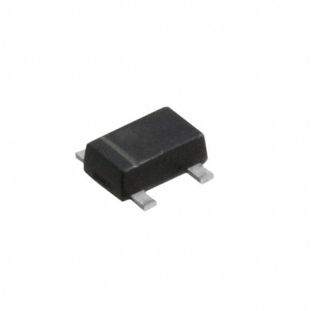
| 描述 | MOSFET P-CH DUAL 30V 9A SOP8MOSFET Pch+Pch -30V -9A MOSFET |
| 产品分类 | FET - 阵列分离式半导体 |
| FET功能 | 逻辑电平门 |
| FET类型 | 2 个 P 沟道(双) |
| Id-ContinuousDrainCurrent | 9 A |
| Id-连续漏极电流 | 9 A |
| 品牌 | Rohm Semiconductor |
| 产品手册 | |
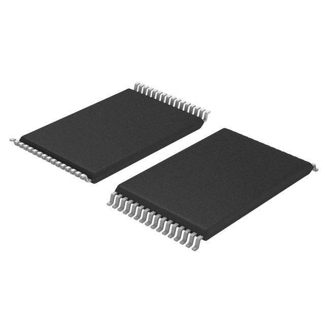
| 产品图片 |
|
| rohs | 符合RoHS无铅 / 符合限制有害物质指令(RoHS)规范要求 |
| 产品系列 | 晶体管,MOSFET,ROHM Semiconductor SH8J66TB1- |
| 数据手册 | |
| 产品型号 | SH8J66TB1 |
| Pd-PowerDissipation | 2 W |
| Pd-功率耗散 | 2 W |
| RdsOn-Drain-SourceResistance | 19 mOhms |
| RdsOn-漏源导通电阻 | 19 mOhms |
| Vds-Drain-SourceBreakdownVoltage | - 30 V |
| Vds-漏源极击穿电压 | - 30 V |
| 不同Id时的Vgs(th)(最大值) | 2.5V @ 1mA |
| 不同Vds时的输入电容(Ciss) | 3000pF @ 10V |
| 不同Vgs时的栅极电荷(Qg) | 35nC @ 5V |
| 不同 Id、Vgs时的 RdsOn(最大值) | 18.5 毫欧 @ 9A,10V |
| 产品目录绘图 |
|
| 产品种类 | MOSFET |
| 供应商器件封装 | 8-SOP |
| 其它名称 | SH8J66TB1DKR |
| 功率-最大值 | 2W |
| 包装 | Digi-Reel® |
| 商标 | ROHM Semiconductor |
| 安装类型 | 表面贴装 |
| 安装风格 | SMD/SMT |
| 封装 | Reel |
| 封装/外壳 | 8-SOIC(0.154",3.90mm 宽) |
| 封装/箱体 | SOP-8 |
| 工厂包装数量 | 2500 |
| 晶体管极性 | P-Channel |
| 最大工作温度 | + 150 C |
| 标准包装 | 1 |
| 正向跨导-最小值 | 11 S |
| 漏源极电压(Vdss) | 30V |
| 特色产品 | http://www.digikey.com/cn/zh/ph/ROHM/MOSFET_ECOMOS.html |
| 电流-连续漏极(Id)(25°C时) | 9A |


- 商务部:美国ITC正式对集成电路等产品启动337调查
- 曝三星4nm工艺存在良率问题 高通将骁龙8 Gen1或转产台积电
- 太阳诱电将投资9.5亿元在常州建新厂生产MLCC 预计2023年完工
- 英特尔发布欧洲新工厂建设计划 深化IDM 2.0 战略
- 台积电先进制程称霸业界 有大客户加持明年业绩稳了
- 达到5530亿美元!SIA预计今年全球半导体销售额将创下新高
- 英特尔拟将自动驾驶子公司Mobileye上市 估值或超500亿美元
- 三星加码芯片和SET,合并消费电子和移动部门,撤换高东真等 CEO
- 三星电子宣布重大人事变动 还合并消费电子和移动部门
- 海关总署:前11个月进口集成电路产品价值2.52万亿元 增长14.8%


PDF Datasheet 数据手册内容提取
SH8J66 4V Drive Pch+Pch MOSFET SH8J66 Structure Dimensions (Unit : mm) Silicon P-channel MOSFET SOP8 Features 1) Low On-resistance. 2) Built-in G-S Protection Diode. 3) Small Surface Mount Package (SOP8). Applications Each lead has same dimensions Switching Packaging specifications Inner circuit Package Taping (8) (7) (6) (5) Type Code TB Basic ordering unit (pieces) 2500 SH8J66 ∗2 ∗2 (1) Tr1 Source ∗1 ∗1 (2) Tr1 Gate Absolute maximum ratings (Ta=25C) (3) Tr2 Source (4) Tr2 Gate <It is the same ratings for Tr1 and Tr2.> (5) Tr2 Drain (1) (2) (3) (4) (6) Tr2 Drain Parameter Symbol Limits Unit ∗1 ESD PROTECTION DIODE (7) Tr1 Drain Drain-source voltage VDSS −30 V ∗2 BODY DIODE (8) Tr1 Drain Gate-source voltage VGSS ±20 V Continuous ID ±9 A Drain current Pulsed IDP ∗1 ±36 A Source current Continuous IS −1.6 A (Body diode) Pulsed ISP ∗1 −36 A Total power dissipation PD ∗2 2.0 W / TOTAL 1.4 W / ELEMENT Channel temperature Tch 150 °C Range of Storage temperature Tstg −55 to +150 °C ∗1 Pw≤10μs, Duty cycle≤1% ∗2 Mounted on a ceramic board www.rohm.com 1/5 2010.01 - Rev.A ○c 2010 ROHM Co., Ltd. All rights reserved.
SH8J66 Data Sheet Electrical characteristics (Ta=25C) <It is the same characteristics for Tr1 and Tr2.> Parameter Symbol Min. Typ. Max. Unit Conditions Gate-source leakage IGSS − − ±10 μA VGS=±20V, VDS=0V Drain-source breakdown voltage V(BR) DSS −30 − − V ID= −1mA, VGS=0V Zero gate voltage drain current IDSS − − −1 μA VDS= −30V, VGS=0V Gate threshold voltage VGS (th) −1.0 − −2.5 V VDS= −10V, ID= −1mA − 13.5 18.5 mΩ ID= −9A, VGS= −10V Static drain-source on-state ∗ resistance RDS (on) − 17.5 23.6 mΩ ID= −4.5A, VGS= −4.5V − 19.0 24.7 mΩ ID= −4.5A, VGS= −4.0V Forward transfer admittance Yfs ∗ 11 − − S VDS= −10V, ID= −9A Input capacitance Ciss − 3000 − pF VDS= −10V Output capacitance Coss − 400 − pF VGS=0V Reverse transfer capacitance Crss − 400 − pF f=1MHz Turn-on delay time td (on) ∗ − 20 − ns VDD −15V TRuisren -toimff edelay time td t(roff) ∗∗ −− 16700 −− nnss RVIDGL==S −=34 .−3.51ΩA0V Fall time tf ∗ − 100 − ns RG=10Ω TGoattael- gsoauterc ceh cahrgaerge QQggs ∗∗ −− 395 −− nnCC VIVDDG=DS − = 9 − A−51V5V Gate-drain charge Qgd ∗ − 12 − nC RL=1.7Ω / RG=10Ω ∗Pulsed Body diode characteristics (Source-drain) (Ta=25C) <It is the same characteristics for Tr1 and Tr2.> Parameter Symbol Min. Typ. Max. Unit Conditions Forward voltage VSD∗ − − −1.2 V IS= −9A, VGS=0V ∗ Pulsed www.rohm.com 2/5 2010.01 - Rev.A ○c 2010 ROHM Co., Ltd. All rights reserved.
SH8J66 Data Sheet Electrical characteristic curves 20 20 100 18 TPua=ls2e5d°C 18 TPau=ls2e5d°C PVuDlSs=e d-10V DRAIN CURRENT : -I[A]D 1111680246 VVVGGGSSS=== ---1440..50VVVVVGGSS== --33..50VV DRAIN CURRENT : -I[A]D 1111680246 VVVGGGSSS=== ---1430..00VVVVGS= -2.5V [A]DRAIN CURRENT : -ID 01.011 TTTTaa==aa == -1 27225555°°°°CCCC 4 VGS= -2.5V 4 2 2 VGS= -2.2V 0 0 0.01 0.0 0.2 0.4 0.6 0.8 1.0 0 2 4 6 8 10 1.0 1.5 2.0 2.5 3.0 DRAIN-SOURCE VOLTAGE : -VDS[V] DRAIN-SOURCE VOLTAGE : -VDS[V] GATE-SOURCE VOLTAGE : -VGS[V] Fig.1 Typical output characteristics() Fig.2 Typical output characteristics() Fig.3 Typical Transfer Characteristics 100 100 100 STATIC DRAIN-SOURCE ON-STATEΩRESISTANCE : R[m]DS(on)10 TPau=ls2e5d°C VVVGGGSSS=== ---441..005VVV STATIC DRAIN-SOURCE ON-STATEΩ[m]RESISTANCE : RDS(on)10 PVuGlSs=e d-10V TTTTaaaa====72 1-5522°°55CC°°CC STATIC DRAIN-SOURCE ON-STATEΩ[m]RESISTANCE : RDS(on)10 VPGulSs=e d-4.5V TTTTaaaa==== 172-25525°°5CC°°CC 1 1 1 0.1 1 10 0.1 1 10 0.1 1 10 DRAIN-CURRENT : -ID[A] DRAIN-CURRENT : -ID[A] DRAIN-CURRENT : -ID[A] Fig.5 Static Drain-Source On-State Fig.6 Static Drain-Source On-State Fig.4 Static Drain-Source On-State Resistance vs. Drain Current() Resistance vs. Drain Current() Resistance vs. Drain Current(I) 100 100 100 E VPGulSs=e d-4.0V E : VPDulSs=e d-10V A] PVuGlSs=e0dV ATIC DRAIN-SOURCE ON-STATΩ[m]RESISTANCE : RDS(on)10 TTTTaa==aa== 1-72225555°°°°CCCC WARD TRANSFER ADMITTANC|Yfs| [S]101 TTTTaaaa==== 271-5522°°55CC°°CC EVERSE DRAIN CURRENT : -Is [ 01.011 TTTTaaaa====1-72225555°°°°CCCC ST OR R 1 F 0 0.01 0.1 1 10 0.1 1 10 0.0 0.2 0.4 0.6 0.8 1.0 1.2 DRAIN-CURRENT : -ID[A] DRAIN-CURRENT : -ID[A] SOURCE-DRAIN VOLTAGE : -VSD [V] Fig.7 Static Drain-Source On-State Fig.8 Forward Transfer Admittance Fig.9 Reverse Drain Current Resistance vs. Drain Current(V) vs. Drain Current vs. Sourse-Drain Voltage www.rohm.com 3/5 2010.01 - Rev.A ○c 2010 ROHM Co., Ltd. All rights reserved.
SH8J66 Data Sheet 50 10000 10 Ta=25°C Ta=25°C STATIC DRAIN-SOURCE ON-STATEΩ[m]RESISTANCE : RDS(on) 12233445050505 ID=ID =-4 -.59A.0A Pulsed Switching Time : t [ns]101001000 tr td(offt)dt(fon) VVRPDGuGDlS=s==1e- 0d-1Ω105VV GATE-SOURCE VOLTAGE : -V [V]GS 2468 PRTVIDuDa=GlD==s -=2e19 5d0-.°0Ω1CA5V 10 1 0 0 5 10 15 0.01 0.1 1 10 0 10 20 30 40 50 60 70 GATE-SOURCE VOLTAGE : -VGS[V] TOTAL GATE CHARGE : Qg [nC] Fig.10 Static Drain-Source On-State FigD.1R1A SINwi-tCchUinRgR CEhNaTra :c -teIDr[iAst]ics Fig.12 Dynamic Input Characteristics Resistance vs. Gate Source Voltage 10000 1000 Operation in this area is limited by RDS(on) (VGS=-10V) 100 Ciss A) PW=100us CAPACITANCE : C [pF]1010000 CCrsosss Tf=a1=M2H5°zC DRAIN CURRENT : -I (D 01.011 Ta = 25°C PPWW= =1 m10sms VGS=0V Single Pulse MOUNTED ON CERAMIC BOARD DC operation 10 0.01 0.01 0.1 1 10 100 0.1 1 10 100 DRAIN-SOURCE VOLTAGE : -VDS[V] DRAIN-SOURCE VOLTAGE : -VDS[V] Fig.14 Maximum Safe Operating Aera Fig.13 Typical Capacitance vs. Drain-Source Voltage L A M R 10 E H NSIENT T CE : r (t) 1 A N 0.1 R A RIZED T RESIST 0.01 SRTRitatnhh =g((ccl eh2h --5Paa°))uC( t=l)s =8e 9 r:(. t31)× U°RCnti/htW(ch-a) MA <Mounted on a CERAMIC board> R 0.001 O N 0.001 0.01 0.1 1 10 100 1000 PULSE WIDTH : Pw(s) Fig.15 Normalized Transient Thermal Resistance vs. Pulse Width www.rohm.com 4/5 2010.01 - Rev.A ○c 2010 ROHM Co., Ltd. All rights reserved.
SH8J66 Data Sheet Measurement circuits Pulse Width VGS ID VDS VGS 10% 50% 90% 50% RL D.U.T. 10% 10% RG VDD 90% 90% VDS td(on) tr td(off) tf ton toff Fig.1-1 Switching Time Test Circuit Fig.1-2 Switching Time Waveforms VG VGS ID VDS Qg IG(Const.) RL VGS D.U.T. RG Qgs Qgd VDD Charge Fig.2-1 Gate Charge Test Circuit Fig.2-2 Gate Charge Waveform www.rohm.com 5/5 2010.01 - Rev.A ○c 2010 ROHM Co., Ltd. All rights reserved.
Notice Notes No copying or reproduction of this document, in part or in whole, is permitted without the consent of ROHM Co.,Ltd. The content specified herein is subject to change for improvement without notice. The content specified herein is for the purpose of introducing ROHM's products (hereinafter "Products"). If you wish to use any such Product, please be sure to refer to the specifications, which can be obtained from ROHM upon request. Examples of application circuits, circuit constants and any other information contained herein illustrate the standard usage and operations of the Products. The peripheral conditions must be taken into account when designing circuits for mass production. Great care was taken in ensuring the accuracy of the information specified in this document. However, should you incur any damage arising from any inaccuracy or misprint of such information, ROHM shall bear no responsibility for such damage. The technical information specified herein is intended only to show the typical functions of and examples of application circuits for the Products. ROHM does not grant you, explicitly or implicitly, any license to use or exercise intellectual property or other rights held by ROHM and other parties. ROHM shall bear no responsibility whatsoever for any dispute arising from the use of such technical information. The Products specified in this document are intended to be used with general-use electronic equipment or devices (such as audio visual equipment, office-automation equipment, commu- nication devices, electronic appliances and amusement devices). The Products specified in this document are not designed to be radiation tolerant. While ROHM always makes efforts to enhance the quality and reliability of its Products, a Product may fail or malfunction for a variety of reasons. Please be sure to implement in your equipment using the Products safety measures to guard against the possibility of physical injury, fire or any other damage caused in the event of the failure of any Product, such as derating, redundancy, fire control and fail-safe designs. ROHM shall bear no responsibility whatsoever for your use of any Product outside of the prescribed scope or not in accordance with the instruction manual. The Products are not designed or manufactured to be used with any equipment, device or system which requires an extremely high level of reliability the failure or malfunction of which may result in a direct threat to human life or create a risk of human injury (such as a medical instrument, transportation equipment, aerospace machinery, nuclear-reactor controller, fuel-controller or other safety device). ROHM shall bear no responsibility in any way for use of any of the Products for the above special purposes. If a Product is intended to be used for any such special purpose, please contact a ROHM sales representative before purchasing. If you intend to export or ship overseas any Product or technology specified herein that may be controlled under the Foreign Exchange and the Foreign Trade Law, you will be required to obtain a license or permit under the Law. Thank you for your accessing to ROHM product informations. More detail product informations and catalogs are available, please contact us. ROHM Customer Support System http://www.rohm.com/contact/ www.rohm.com R0039A © 2009 ROHM Co., Ltd. All rights reserved.