
 Datasheet下载
- 型号: LM139APT
- 制造商: STMicroelectronics
- 库位|库存: xxxx|xxxx
- 要求:
| 数量阶梯 | 香港交货 | 国内含税 |
| +xxxx | $xxxx | ¥xxxx |
查看当月历史价格
查看今年历史价格
LM139APT产品简介:
ICGOO电子元器件商城为您提供LM139APT由STMicroelectronics设计生产,在icgoo商城现货销售,并且可以通过原厂、代理商等渠道进行代购。 LM139APT价格参考。STMicroelectronicsLM139APT封装/规格:线性 - 比较器, 通用 比较器 CMOS,DTL,ECL,MOS,开路集电极,TTL 14-TSSOP。您可以下载LM139APT参考资料、Datasheet数据手册功能说明书,资料中有LM139APT 详细功能的应用电路图电压和使用方法及教程。
STMicroelectronics的LM139APT是一款四通道电压比较器,属于线性比较器类别。它广泛应用于需要将两个电压信号进行比较并根据比较结果输出高低电平的电子系统中。

典型应用场景包括:

1. 电压检测与监控:用于电源管理系统中,监测电池或电源电压是否低于或高于设定阈值,从而触发报警或保护机制。

2. 过温保护电路:配合温度传感器使用,当检测到温度超过设定值时,比较器输出信号以关闭设备或启动冷却装置。

3. 窗口比较器:通过组合多个比较器,判断输入信号是否处于某一电压范围内,常用于模拟信号的合格判定。

4. 波形整形与转换:用于将正弦波、三角波等模拟信号转换为方波,适用于数字系统的输入接口。

5. 自动控制系统:在工业控制和自动化设备中,作为传感器信号处理的一部分,实现开关控制功能。

LM139APT具有低功耗、宽工作电压范围(2V至36V)以及可直接驱动TTL/CMOS电路等特点,适合多种通用比较应用场合。
| 参数 | 数值 |
| 产品目录 | 集成电路 (IC)半导体 |
| CMRR,PSRR(典型值) | - |
| 描述 | IC COMPARATOR QUAD LP 14-TSSOP模拟比较器 Low-Power Quad 1.1 mA 25nA |
| 产品分类 | |
| 品牌 | STMicroelectronics |
| 产品手册 | |
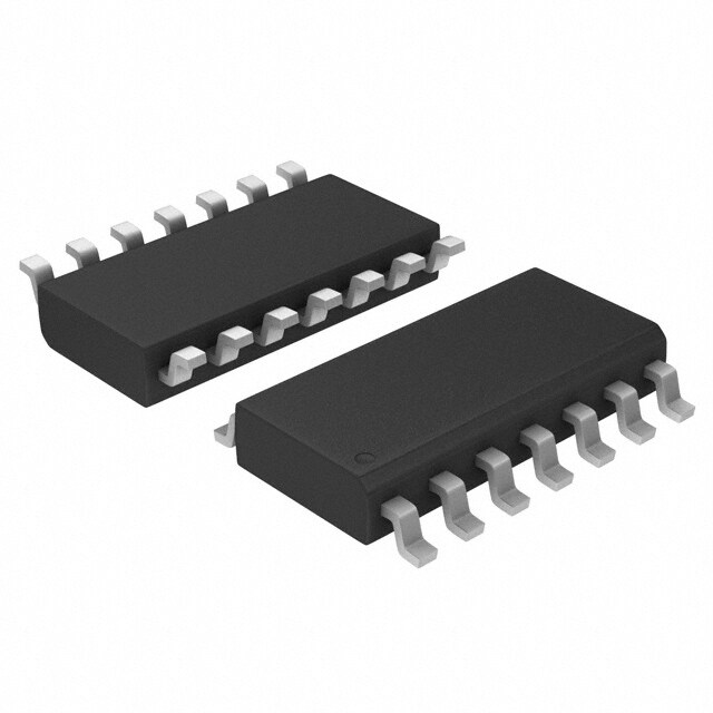
| 产品图片 |
|
| rohs | 符合RoHS无铅 / 符合限制有害物质指令(RoHS)规范要求 |
| 产品系列 | 模拟比较器,STMicroelectronics LM139APT- |
| 数据手册 | |
| 产品型号 | LM139APT |
| 产品 | Analog Comparators |
| 产品种类 | 模拟比较器 |
| 传播延迟(最大值) | - |
| 供应商器件封装 | 14-TSSOP |
| 偏转电压—最大值 | 2 mV |
| 元件数 | 4 |
| 其它名称 | 497-10614-6 |
| 包装 | Digi-Reel® |
| 响应时间 | 1.3 us |
| 商标 | STMicroelectronics |
| 安装类型 | 表面贴装 |
| 安装风格 | SMD/SMT |
| 封装 | Reel |
| 封装/外壳 | 14-TSSOP(0.173",4.40mm 宽) |
| 封装/箱体 | TSSOP-14 |
| 工作温度 | -55°C ~ 125°C |
| 工厂包装数量 | 2500 |
| 最大工作温度 | + 125 C |
| 最小工作温度 | - 55 C |
| 标准包装 | 1 |
| 滞后 | - |
| 电压-电源,单/双 (±) | 2 V ~ 32 V, ±1 V ~ 16 V |
| 电压-输入失调(最大值) | 2mV @ 30V |
| 电流-输入偏置(最大值) | 0.1µA @ 5V |
| 电流-输出(典型值) | 16mA @ 5V |
| 电流-静态(最大值) | 2mA |
| 电源电压-最大 | 36 V |
| 电源电压-最小 | 2 V |
| 电源电流 | 1.1 mA |
| 电源电流—最大值 | 1.1 mA |
| 类型 | 通用 |
| 系列 | LM139 |
| 输入偏压电流—最大 | 300 nA |
| 输出类型 | CMOS,DTL,ECL,MOS,开路集电极,TTL |


- 商务部:美国ITC正式对集成电路等产品启动337调查
- 曝三星4nm工艺存在良率问题 高通将骁龙8 Gen1或转产台积电
- 太阳诱电将投资9.5亿元在常州建新厂生产MLCC 预计2023年完工
- 英特尔发布欧洲新工厂建设计划 深化IDM 2.0 战略
- 台积电先进制程称霸业界 有大客户加持明年业绩稳了
- 达到5530亿美元!SIA预计今年全球半导体销售额将创下新高
- 英特尔拟将自动驾驶子公司Mobileye上市 估值或超500亿美元
- 三星加码芯片和SET,合并消费电子和移动部门,撤换高东真等 CEO
- 三星电子宣布重大人事变动 还合并消费电子和移动部门
- 海关总署:前11个月进口集成电路产品价值2.52万亿元 增长14.8%


PDF Datasheet 数据手册内容提取
LM139, LM239, LM339 Low-power quad voltage comparators Datasheet - production data Features • Wide single supply voltage range or dual supplies for all devices: +2 to +36 V or ±1 V to ±18 V D • Very low supply current (1.1 mA) independent SO14 of supply voltage (plastic micropackage) • Low input bias current: 25 nA typ • Low input offset current: ±5 nA typ • Low input offset voltage: ±1 mV typ • Input common-mode voltage range includes ground P TSSOP14 • Low output saturation voltage: 250 mV typ; (thin shrink small outline package) (ISINK = 4 mA) • Differential input voltage range equal to the supply voltage • TTL, DTL, ECL, MOS, CMOS compatible outputs Q Description QFN16 3x3 (plastic micropackage) This family of devices consists of four independent precision-voltage comparators with an offset voltage specification as low as 2 mV maximum for LM339A, LM239A, and LM139A. Each comparator has been designed specifically to operate from a single power supply over a wide range of voltages. Operation from split power supplies is also possible. These comparators also have a unique characteristic in that the input common mode voltage range includes ground even though operated from a single power supply voltage. August 2014 DocID2159 Rev 4 1/19 This is information on a product in full production. www.st.com
Contents LM139, LM239, LM339 Contents 1 Pin and schematic diagram . . . . . . . . . . . . . . . . . . . . . . . . . . . . . . . . . . . 3 2 Absolute maximum ratings and operating conditions . . . . . . . . . . . . . 4 3 Electrical characteristics . . . . . . . . . . . . . . . . . . . . . . . . . . . . . . . . . . . . . 6 4 Electrical characteristics curves . . . . . . . . . . . . . . . . . . . . . . . . . . . . . . . 8 5 Typical applications . . . . . . . . . . . . . . . . . . . . . . . . . . . . . . . . . . . . . . . . . 9 6 Package information . . . . . . . . . . . . . . . . . . . . . . . . . . . . . . . . . . . . . . . . 12 6.1 SO14 package information . . . . . . . . . . . . . . . . . . . . . . . . . . . . . . . . . . . . 13 6.2 TSSOP14 package information . . . . . . . . . . . . . . . . . . . . . . . . . . . . . . . . 14 6.3 QFN16 3x3 package information . . . . . . . . . . . . . . . . . . . . . . . . . . . . . . . 15 7 Ordering information . . . . . . . . . . . . . . . . . . . . . . . . . . . . . . . . . . . . . . . 17 8 Revision history . . . . . . . . . . . . . . . . . . . . . . . . . . . . . . . . . . . . . . . . . . . 18 2/19 DocID2159 Rev 4
LM139, LM239, LM339 Pin and schematic diagram 1 Pin and schematic diagram Figure 1. Pin connections (top view) Output2 1 14 Output3 Output1 2 13 Output4 VCC+ 3 12 VCC- Invertinginput1 4 11 Non-invertinginput4 Non-invertinginput1 5 10 Invertinginput4 Invertinginput2 6 9 Non-invertinginput3 Non-invertinginput2 7 8 Invertinginput3 Figure 2. Schematic diagram (1/4 LM139) V CC 3.5μA 100 μA 3.5μA 100μA Non-inverting input V O Inverting input V CC DocID2159 Rev 4 3/19 19
Absolute maximum ratings and operating conditions LM139, LM239, LM339 2 Absolute maximum ratings and operating conditions Table 1. Absolute maximum ratings Symbol Parameter Value Unit V Supply voltage ±18 or 36 V CC V Differential input voltage ±36 V ID V Input voltage -0.3 to +36 V IN Output short-circuit to ground(1) Infinite Thermal resistance junction to ambient(2) SO14 105 R °C/W thja TSSOP14 100 QFN16 3x3 45 Thermal resistance junction to case(2) SO14 31 R °C/W thjc TSSOP14 32 QFN16 3x3 14 T Storage temperature range -65 to +150 °C stg T Junction temperature +150 °C j T Lead temperature (soldering 10 seconds) 260 °C LEAD Human body model (HBM)(3) 500 ESD Machine model (MM)(4) 100 V Charged device model (CDM)(5) 1500 1. Short-circuits from the output to V + can cause excessive heating and eventual destruction. The maximum output current is approxCimCately 20 mA independent of the magnitude of V +. CC 2. Short-circuits can cause excessive heating. These values are typical. 3. Human body model: a 100 pF capacitor is charged to the specified voltage, then discharged through a 1.5 kΩ resistor between two pins of the device. This is done for all couples of connected pin combinations while the other pins are floating. 4. Machine model: a 200 pF capacitor is charged to the specified voltage, then discharged directly between two pins of the device with no external series resistor (internal resistor < 5 Ω). This is done for all couples of connected pin combinations while the other pins are floating. 5. Charged device model: all pins and the package are charged together to the specified voltage and then discharged directly to the ground through only one pin. This is done for all pins. 4/19 DocID2159 Rev 4
LM139, LM239, LM339 Absolute maximum ratings and operating conditions Table 2. Operating conditions (T = 25 °C) amb Symbol Parameter Value Unit 2 to 32 V Supply voltage V CC ±1 to ±16 V Common mode input voltage range 0 to (V + - 1.5) V ICM CC Operating free-air temperature range – LM139, LM139A -55, +125 T °C oper – LM239, LM239A -40, +105 – LM339, LM339A 0, +70 DocID2159 Rev 4 5/19 19
Electrical characteristics LM139, LM239, LM339 3 Electrical characteristics T a ble 3. Electrical characteristics at V + = +5 V, V - = GND, T = +25 °C CC CC amb (unless otherwise specified) LM139A - LM239A LM139 - LM239 LM339A LM339 Symbol Parameter Unit Min. Typ. Max. Min Typ. Max. Input offset voltage(1) 1 2 1 5 mV V IO T ≤ T ≤ T 4 9 min amb max Input offset current 3 25 5 50 nA I IO T ≤ T ≤ T 100 150 min amb max Input bias current (I+ or I-)(2) 25 100 25 250 nA I IB T ≤ T ≤ T 300 400 min amb max Large signal voltage gain A VD V = 15 V, R = 15 kΩ, V = 1 V to 11 V 50 200 50 200 V/mV CC L o Supply current (all comparators) ICC VCC = +5 V, no load 1.1 2 1.1 2 mA V = +30 V, no load 1.3 2.5 1.3 2.5 CC Input common mode voltage range(3) VICM VCC = 30 V 0 VCC+ -1.5 0 VCC+ -1.5 V Tmin ≤ Tamb ≤ Tmax 0 VCC+ -2 0 VCC+ -2 V Differential input voltage (4) V + V + V ID CC CC Low level output voltage VOL VID = -1 V, ISINK = 4 mA 250 400 250 400 mV T ≤ T ≤ T 700 700 min amb max High level output current IOH VCC = Vo = 30 V, VID = 1 V 0.1 0.1 nA T ≤ T ≤ T 1 1 μA min amb max Output sink current I SINK V = 1 V, V = 1.5 V 6 16 6 16 mA ID o Response time (5) t re R = 5.1 kΩ connected to V + 1.3 1.3 μs L CC 6/19 DocID2159 Rev 4
LM139, LM239, LM339 Electrical characteristics Table 3. Electrical characteristics at V + = +5 V, V - = GND, T = +25 °C CC CC amb (unless otherwise specified) (continued) LM139A - LM239A LM139 - LM239 LM339A LM339 Symbol Parameter Unit Min. Typ. Max. Min Typ. Max. Large signal response time trel R = 5.1 kΩ connected to V +, e = TTL, L CC l V = +1.4 V 300 300 ns (ref) 1. At output switch point, V ≈ 1.4 V, V + from 5 V to 30 V, and over the full common-mode range (0 V to V + -1.5 V). o CC CC 2. The direction of the input current is out of the IC due to the PNP input stage. This current is essentially constant, independent of the state of the output, so no loading charge exists on the reference of input lines. 3. The input common-mode voltage of either input signal voltage should not be allowed to go negative by more than 0.3 V. The upper end of the common-mode voltage range is V + -1.5 V, but either or both inputs can go to +30 V without CC damage. 4. Positive excursions of input voltage may exceed the power supply level. As long as the other voltage remains within the common-mode range, the comparator will provide a proper output state. The low input voltage state must not be less than -0.3 V (or 0.3 V below the negative power supply, if used). 5. The response time specified is for a 100 mV input step with 5 mV overdrive. For larger overdrive signals, 300 ns can be obtained. DocID2159 Rev 4 7/19 19
Electrical characteristics curves LM139, LM239, LM339 4 Electrical characteristics curves Figure 3. Supply current vs. supply voltage Figure 4. Input current vs. supply voltage 1 80 (mA) 0.8 TamTba=mb-5=5°0C°C nA) 60 RVii==01V09Ω Tamb=-55°C T ( REN 0.6 Tamb=+25°C ENT Tamb=0°C UR Tamb=+70°C RR 40 Tamb=+25°C YC 0.4 CU PL Tamb=+125°C UT 20 UP 0.2 NP Tamb=+125°C S R = I Tamb=+70°C 0 10 20 30 40 0 10 20 30 40 SUPPLYVOLTAGE(V) SUPPLYVOLTAGE(V) Figure 5. Output saturation voltage vs. output Figure 6. Response time for various input current overdrives - negative transition 101 6 VOLTAGE(V) 1100-01 Tamb=+OO12uu5tt°ooCffssaattuurraattiioonn OLTAGE(mV) VOLTAGE(V) 54321 2100m0mIVnVputoverdrive:5mV eI 5V e5o.1kΩ N V T TURATIO 10-2 Tamb=+2T5a°mCb=-55°C INPUT OUTPU -1-050000 Tamb=+25°C A S 10-3 10-2 10-1 100 101 102 0 0.5 1 1.5 2 TIME(μs) OUTPUTSINKCURRENT(mA) Figure 7. Response time for various input overdrives - positive transition 6 V) V)1 5 Inputoverdrive:100mV m ( GE( AGE 43 5mV TA OLT 2 OL V 1 20mV V T 5V INPUT OUTPU 50000 Tamb=+25°C eI 5e.o1kΩ 0 0 0.5 1 1.5 2 TIME(μs) 8/19 DocID2159 Rev 4
LM139, LM239, LM339 Typical applications 5 Typical applications Figure 8. Basic comparator Figure 9. Driving CMOS 5 V V = 5 V CC 15 kΩ 100 kΩ +V +V (ref) (ref) 1/4 & 1/4 LM139 V LM139 O -V -V (ref) (ref) Figure 10. Driving TTL Figure 11. Low frequency op amp 5 V 5 V 15 kΩ 10 kΩ 1/4 LM139 +V (ref) ~ e 1/4 & l e o LM139 -V 100 kΩ 0.5 μF (ref) 1 kΩ & A = 100 V Figure 12. Low frequency op amp Figure 13. Transducer amplifier 5 V 5 V (e = 0 V for e = 0 V) o l 15 kΩ Magnetic pick-up 10 kΩ 3 kΩ 1/4 LM139 2N 2222 1/4 ~ el 0.5 μF LM139 eo 20 MΩ 100 kΩ 1 kΩ eo 10 kΩ A = 100 V DocID2159 Rev 4 9/19 19
Typical applications LM139, LM239, LM339 Figure 14. Time delay generator VCC=+15V 10 kΩ 15 kΩ 200 kΩ 3 kΩ 10 MΩ 10 kΩ V3 LM1/1439 V03 VCtoC t3 3kΩ 10 kΩ 51 kΩ 10 MΩ VCC L1M/4139 VC1 10 kΩ 0to tA V(ref.) V2 LM1/1439 VO2 VtCoC t2 Input gating signal 0.001μF 3 kΩ VCC 10 MΩ 51 kΩ 10 kΩ 1/4 VC1VVV123 V1 LM139 VO1 VCCt0 t1 0t0t1t2 t3 t4 t 51 kΩ Figure 15. Low frequency op amp with offset Figure 16. Zero crossing detector adjust (single power supply) 5 V 5 V Offset adjust 100 kΩ 5 V 100 kΩ 100 kΩ 5.1 kΩ RS R2 R1 1 MΩ 1 MΩ15 kΩ e 5.1 kΩ 5.1 kΩ l e ~ L1M/1439 2N 2222 L1M/1439 l 0.5μF 1N4148 R1 100 kΩ 1 kΩ 20 MΩ e 10 kΩ o Figure 17. Two-decade high-frequency VCO VCC 100 kΩ VCC 100 kΩ 500 pF 3 kΩ 3 kΩ FrevqouVlteacngoceny ti rncopolunttrol 0.1 μF LM1/1439 05.0.11 kμΩF L1M/1439 Output 1 20 kΩ VCC/2 Output 2 50 kΩ 20 kΩ 1/4 VCC/2 LM139 VCC=+30V +250 mV Vcontrol +50 V 700 Hz fo 100 kHz 10/19 DocID2159 Rev 4
LM139, LM239, LM339 Typical applications Figure 18. Limit comparator Figure 19. Crystal-controlled oscillator V (12 V) V = 15 V CC CC 2R 10 kΩ 200 kΩ 2 kΩ S V 100 kΩ (ref) high 1/4 LM139 V Lamp CC RS 0.1 μF L1M/1439 eo 0 e ~ I f = 100 kHz 1/4 2R LM139 2N2222 200 kΩ S V (ref) low Figure 20. Zero crossing detector Figure 21. Comparator with a negative reference 15 V 15 V 5.1 kΩ 5.1 kΩ 1/4 e 1/4 e LM139 o LM139 o e ~ e ~ I I 5 V 15 V 15 V DocID2159 Rev 4 11/19 19
Package information LM139, LM239, LM339 6 Package information In order to meet environmental requirements, ST offers these devices in different grades of ECOPACK® packages, depending on their level of environmental compliance. ECOPACK® specifications, grade definitions and product status are available at: www.st.com. ECOPACK® is an ST trademark. 12/19 DocID2159 Rev 4
LM139, LM239, LM339 Package information 6.1 SO14 package information Figure 22. SO14 package mechanical drawing Table 4. SO14 package mechanical data Dimensions Millimeters Inches Ref. Min. Typ. Max. Min. Typ. Max. A 1.35 1.75 0.05 0.068 A1 0.10 0.25 0.004 0.009 A2 1.10 1.65 0.04 0.06 B 0.33 0.51 0.01 0.02 C 0.19 0.25 0.007 0.009 D 8.55 8.75 0.33 0.34 E 3.80 4.0 0.15 0.15 e 1.27 0.05 H 5.80 6.20 0.22 0.24 h 0.25 0.50 0.009 0.02 L 0.40 1.27 0.015 0.05 k 8° (max.) ddd 0.10 0.004 DocID2159 Rev 4 13/19 19
Package information LM139, LM239, LM339 6.2 TSSOP14 package information Figure 23. TSSOP14 package mechanical drawing Table 5. TSSOP14 package mechanical data Dimensions Ref. Millimeters Inches Min. Typ. Max. Min. Typ. Max. A 1.20 0.047 A1 0.05 0.15 0.002 0.004 0.006 A2 0.80 1.00 1.05 0.031 0.039 0.041 b 0.19 0.30 0.007 0.012 c 0.09 0.20 0.004 0.0089 D 4.90 5.00 5.10 0.193 0.197 0.201 E 6.20 6.40 6.60 0.244 0.252 0.260 E1 4.30 4.40 4.50 0.169 0.173 0.176 e 0.65 0.0256 L 0.45 0.60 0.75 0.018 0.024 0.030 L1 1.00 0.039 k 0° 8° 0° 8° aaa 0.10 0.004 14/19 DocID2159 Rev 4
LM139, LM239, LM339 Package information 6.3 QFN16 3x3 package information Figure 24. QFN16 3x3 package mechanical drawing DocID2159 Rev 4 15/19 19
Package information LM139, LM239, LM339 Table 6. QFN16 3x3 mm package mechanical data (pitch 0.5 mm) Dimensions Ref. Millimeters Inches Min. Typ. Max. Min. Typ. Max. A 0.80 0.90 1.00 0.031 0.035 0.039 A1 0 0.05 0 0.002 A3 0.20 0.008 b 0.18 0.30 0.007 0.012 D 2.90 3.00 3.10 0.114 0.118 0.122 D2 1.50 1.80 0.059 0.071 E 2.90 3.00 3.10 0.114 0.118 0.122 E2 1.50 1.80 0.059 0.071 e 0.50 0.020 L 0.30 0.50 0.012 0.020 Figure 25. QFN16 3x3 footprint recommendation 16/19 DocID2159 Rev 4
LM139, LM239, LM339 Ordering information 7 Ordering information Table 7. Order codes Temperature Part number Package Packing Marking range LM139DT 139 SO14 LM139ADT 139A -55 °C, +125 °C LM139PT 139 TSSOP14 LM139APT 139A LM239DT 239 SO14 LM239ADT 239A LM239PT -40 °C, +105 °C 239 TSSOP14 Tape and reel LM239APT 239A LM239QT QFN16 3x3 K550 LM339DT 339 SO14 LM339ADT 339A LM339PT 0 °C, +70 °C 339 TSSOP14 LM339APT 339A LM339QT QFN16 3x3 K551 DocID2159 Rev 4 17/19 19
Revision history LM139, LM239, LM339 8 Revision history Table 8. Document revision history Date Revision Changes 01-Mar-2003 1 Initial release. Updated document format. Removed power dissipation from Table 1: Absolute maximum ratings. 28-Apr-2009 2 Added R , R ESD and T valuesto Table 1. THJA THJC, LEAD Updated package information in Chapter 6. Added Table 7: Order codes. Added pin connections for QFN16 package in Figure 1 on page 3. Added thermal information for QFN16 package in Table 1 on page 4. 13-Jul-2011 3 Added QFN16 package information in Chapter 6. Added order codes for QFN16 package in Table 7: Order codes. Removed DIP14 package Table 7: Order codes: replaced the marking of the order code 18-Aug-2014 4 LM239QT from K549 to K550; removed all order codes with “tube” packing. Updated disclaimer 18/19 DocID2159 Rev 4
LM139, LM239, LM339 IMPORTANT NOTICE – PLEASE READ CAREFULLY STMicroelectronics NV and its subsidiaries (“ST”) reserve the right to make changes, corrections, enhancements, modifications, and improvements to ST products and/or to this document at any time without notice. Purchasers should obtain the latest relevant information on ST products before placing orders. ST products are sold pursuant to ST’s terms and conditions of sale in place at the time of order acknowledgement. Purchasers are solely responsible for the choice, selection, and use of ST products and ST assumes no liability for application assistance or the design of Purchasers’ products. No license, express or implied, to any intellectual property right is granted by ST herein. Resale of ST products with provisions different from the information set forth herein shall void any warranty granted by ST for such product. ST and the ST logo are trademarks of ST. All other product or service names are the property of their respective owners. Information in this document supersedes and replaces information previously supplied in any prior versions of this document. © 2014 STMicroelectronics – All rights reserved DocID2159 Rev 4 19/19 19