ICGOO在线商城 > SG3842DM

 Datasheet下载
- 型号: SG3842DM
- 制造商: American Microsemiconductor, Inc.
- 库位|库存: xxxx|xxxx
- 要求:
| 数量阶梯 | 香港交货 | 国内含税 |
| +xxxx | $xxxx | ¥xxxx |
查看当月历史价格
查看今年历史价格
SG3842DM产品简介:
ICGOO电子元器件商城为您提供SG3842DM由American Microsemiconductor, Inc.设计生产,在icgoo商城现货销售,并且可以通过原厂、代理商等渠道进行代购。 提供SG3842DM价格参考以及American Microsemiconductor, Inc.SG3842DM封装/规格参数等产品信息。 你可以下载SG3842DM参考资料、Datasheet数据手册功能说明书, 资料中有SG3842DM详细功能的应用电路图电压和使用方法及教程。
| 参数 | 数值 |
| 产品目录 | 集成电路 (IC) |
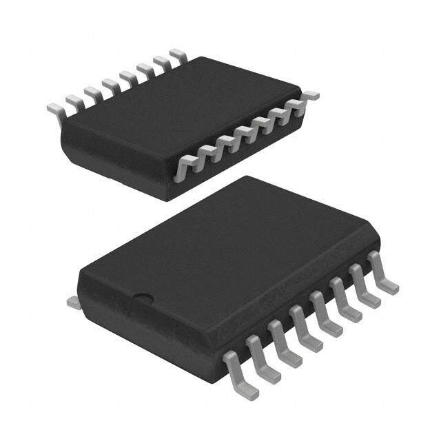
| 描述 | IC REG CTRLR FLYBK ISO PWM 8SOIC |
| 产品分类 | |
| 品牌 | Microsemi Analog Mixed Signal Group |
| 数据手册 | http://www.microsemi.com/document-portal/doc_download/11137-sg1842-pdf |
| 产品图片 |
|
| 产品型号 | SG3842DM |
| rohs | 无铅 / 符合限制有害物质指令(RoHS)规范要求 |
| 产品系列 | - |
| 产品目录页面 | |
| 供应商器件封装 | 8-SOIC |
| 功率(W) | - |
| 包装 | 散装 |
| 封装/外壳 | * |
| 工作温度 | 0°C ~ 70°C |
| 标准包装 | 2,500 |
| 电压-击穿 | - |
| 电压-输入 | 10 V ~ 30 V |
| 电压-输出 | 13.5V |
| 输出隔离 | 隔离 |
| 频率范围 | 100Hz ~ 500kHz |


- 商务部:美国ITC正式对集成电路等产品启动337调查
- 曝三星4nm工艺存在良率问题 高通将骁龙8 Gen1或转产台积电
- 太阳诱电将投资9.5亿元在常州建新厂生产MLCC 预计2023年完工
- 英特尔发布欧洲新工厂建设计划 深化IDM 2.0 战略
- 台积电先进制程称霸业界 有大客户加持明年业绩稳了
- 达到5530亿美元!SIA预计今年全球半导体销售额将创下新高
- 英特尔拟将自动驾驶子公司Mobileye上市 估值或超500亿美元
- 三星加码芯片和SET,合并消费电子和移动部门,撤换高东真等 CEO
- 三星电子宣布重大人事变动 还合并消费电子和移动部门
- 海关总署:前11个月进口集成电路产品价值2.52万亿元 增长14.8%


PDF Datasheet 数据手册内容提取
SG1842/SG1843 Series ® CURRENT MODE PWM CONTROLLER TM P R O D U C T I O N D A T A S H E E T DESCRIPTION KEY FEATURES The SG1842/43 family of control IC's provides all lockout, current limiting circuitry and start-up (cid:132) OPTIMIZED FOR OFF-LINE the necessary features to implement off-line fixed current of less than 1mA. The totem-pole output CONTROL frequency, current-mode switching power supplies is optimized to drive the gate of a power (cid:132) LOW START-UP CURRENT (<1mA) with a minimum number of external components. MOSFET. The output is low in the off state to (cid:132) AUTOMATIC FEED FORWARD Current-mode architecture demonstrates improved provide direct interface to an N channel device. COMPENSATION (cid:132) TRIMMED OSCILLATOR line regulation, improved load regulation, pulse- The SG1842/43 is specified for operation over DISCHARGE CURRENT by-pulse current limiting and inherent protection the full military ambient temperature range of - (cid:132) PULSE-BY-PULSE CURRENT of the power supply output switch. The bandgap 55°C to 125°C. The SG2842/43 is specified for LIMITING reference is trimmed to ±1% over temperature. the industrial range of -25°C to 85°C, and the (cid:132) ENHANCED LOAD RESPONSE Oscillator discharge current is trimmed to less SG3842/43 is designed for the commercial range CHARACTERISTICS than ±10%. The SG1842/43 has under-voltage of 0°C to 70°C. (cid:132) UNDER-VOLTAGE LOCKOUT WITH 6V HYSTERESIS (SG1842 only) (cid:132) DOUBLE-PULSE SUPPRESSION IMPORTANT: For the most current data, consult MICROSEMI’s website: http://www.microsemi.com (cid:132) HIGH-CURRENT TOTEM-POLE OUTPUT (1AMP PEAK) (cid:132) INTERNALLY TRIMMED BANDGAP PRODUCT HIGHLIGHT REFERENCE (cid:132) 500KHZ OPERATION (cid:132) UNDERVOLTAGE LOCKOUT R ST SG1842 - 16 volts SG1843 - 8.4 volts (cid:132) LOW SHOOT-THROUGH I CURRENT <75mA OVER AC ST TEMPERATURE INPUT V CC HIGH RELIABILITY FEATURES SG3842 (cid:132) AVAILABLE TO MIL-STD-883B AND DSCC (cid:132) SCHEDULED FOR MIL-M38510 QPL LISTING (cid:132) RADIATION DATA AVAILABLE (cid:132) Microsemi LEVEL "S" PROCESSING AVAILABLE PACKAGE ORDER INFO Plastic DIP Plastic DIP Plastic SOIC Plastic SOIC Ceramic Dip Ceramic DIP Cer Flatpack Ceramic LCC T (°C) M 8-Pin N 14-Pin DM 8-Pin D 14-Pin Y 8-Pin J 14-Pin F 10-Pin L 20-Pin A RoHS / Pb-free Transition DC: 0503 RoHS / Pb-free Transition DC:0440 SG3842M SG3842N SG3842DM SG3842D SG3842Y SG3842J 0 to 70 SG3843M SG3843N SG3843DM SG3843D SG3843Y SG3842J SG2842M SG2842N SG2842DM SG2842D SG2842Y SG2842J -25 to 85 SG2843M SG2843N SG2843DM SG2843D SG2843Y SG2843J -55 to SG1842Y SG1842J SG1842F SG1842L 125 SG1843Y SG1843J SG1843F SG1842L MIL- SG1842Y/883B SG1842J/883B SG1842F/883B SG1842L/883B STD/883 SG1843Y/883B SG1843J/883B SG1843F/883B SG1843L/883B SG1842Y/DESC SG1842J/DESC SG1842F/DESC SG1842L/DESC DESC SG1843Y/DESC SG1843J/DESC SG1843F/DESC SG1843L/DESC Note: Available in Tape & Reel. Append the letters “TR” to the part number. (i.e. SG2843DM-TR) Plastic packages are RoHS compliant Copyright © 2000 Microsemi 1 Rev. 1.6b 2010-03-15 Analog Mixed Signal Group 11861 Western Avenue, Garden Grove, CA. 92841, 714-898-8121, Fax: 714-893-2570
P R O D U C T D A T A B O O K 1 9 9 6 / 1 9 9 7 SG1842/SG1843 Series CURRENT-MODE PWM CONTROLLER P R O D U C T I O N D A T A S H E E T ABSOLUTE MAXIMUM RATINGS (Notes 1 & 2) PACKAGE PIN OUTS Supply Voltage (I < 30mA)...............................................................Self Limiting CC Supply Voltage (Low Impedance Source)........................................................30V COMP 1 8 V REF Output Current (Peak).......................................................................................±1A VFB 2 7 VCC Output Current (Continuous).......................................................................350mA ISENSE 3 6 OUTPUT R/C 4 5 GND Output Energy (Capacitive Load).......................................................................5µJ T T Analog Inputs (Pins 2, 3).................................................................-0.3V to +6.3V M & Y PACKAGE Error Amp Output Sink Current.....................................................................10mA (Top View) M Package: Pb-free / RoHS 100% Matte Tin Lead Finish Power Dissipation at T = 25°C (DIL-8) ............................................................1W A Operating Junction Temperature COMP 1 8 V REF Hermetic (J, Y, F, L Packages)...................................................................150°C VFB 2 7 VCC I 3 6 OUTPUT Plastic (N, M, D, DM Packages) ................................................................150°C SENSE R/C 4 5 GND Storage Temperature Range..........................................................-65°C to +150°C T T Lead Temperature (Soldering, 10 Seconds)..................................................300°C DM PACKAGE Pb-free / RoHS Peak Package Solder Reflow Temp. (40 second max. exposure)........ 260°C (+0, -5) (Top View) Pb-free / RoHS 100% Matte Tin Lead Finish Note 1. Exceeding these ratings could cause damage to the device. Note 2. All voltages are with respect to Pin 5. All currents are positive into the specified COMP 1 14 VREF terminal. N.C. 2 13 N.C. V 3 12 V FB CC THERMAL DATA N.C. 4 11 V C I 5 10 OUTPUT SENSE M PACKAGE: N.C. 6 9 GND R/C 7 8 PWR GND THERMAL RESISTANCE-JUNCTION TO AMBIENT, θθθθθ 95°C/W T T JA D PACKAGE N PACKAGE: (Top View) THERMAL RESISTANCE-JUNCTION TO AMBIENT, θθθθθ 65°C/W Pb-free / RoHS 100% Matte Tin Lead Finish JA DM PACKAGE: COMP 1 14 VREF N.C. 2 13 N.C. THERMAL RESISTANCE-JUNCTION TO AMBIENT, θθθθθ 165°C/W JA VFB 3 12 VCC D PACKAGE: N.C. 4 11 V C THERMAL RESISTANCE-JUNCTION TO AMBIENT, θθθθθ 120°C/W ISENSE 5 10 OUTPUT JA N.C. 6 9 GROUND Y PACKAGE: R/C 7 8 POWER GND T T THERMAL RESISTANCE-JUNCTION TO AMBIENT, θθθθθ 130°C/W J & N PACKAGE JA J PACKAGE: (Top View) N Package: Pb-free / RoHS 100% Matte Tin Lead Finish THERMAL RESISTANCE-JUNCTION TO AMBIENT, θθθθθ 80°C/W JA 1.COMP 10.V F PACKAGE: 2.VFB 12 109 9. VRCECF THERMAL RESISTANCE-JUNCTION TO CASE, θθθθθJC 80°C/W 34..IRSTE/NSCET 345 876 87.. VOCUTPUT THERMAL RESISTANCE-JUNCTION TO AMBIENT, θθθθθ 145°C/W 5.POWER GND 6. GND JA L PACKAGE: F PACKAGE THERMAL RESISTANCE-JUNCTION TO CASE, θθθθθ 35°C/W JC (Top View) THERMAL RESISTANCE-JUNCTION TO AMBIENT, θθθθθ 120°C/W JA Junction Temperature Calculation: T = T + (P x θ ). 3 2 1 20 19 1. N.C. 11.N.C. The θJA numbers are guidelines for thJe theArmal DperfoJArmance of the device/pc-board 4 18 23.. NCO.CM.P 1123..GNR.CO.UND system. All of the above assume no ambient airflow. 4. N.C. 14.N.C. 5 17 5. V 15.OUTPUT 6 16 6. NF.BC. 16.N.C. 7 15 7. I 17.V SENSE CC 8 14 8. N.C. 18.N.C. 9. N.C. 19.N.C. 10. R/C 20.V 9 10 11 12 13 T T REF L PACKAGE (Top View) 2 Copyright © 2000 Rev. 1.6a 10/04
P R O D U C T D A T A B O O K 1 9 9 6 / 1 9 9 7 SG1842/SG1843 Series CURRENT-MODE PWM CONTROLLER P R O D U C T I O N D A T A S H E E T RECOMMENDED OPERATING CONDITIONS (Note 3) Recommended Operating Conditions Parameter Symbol Units Min. Typ. Max. Supply Voltage Range 30 V Output Current (Peak) ±1 A Output Current (Continuous) 200 mA Analog Inputs (Pin 2, Pin 3) 0 2.6 V Error Amp Output Sink Current 5 mA Oscillator Frequency Range 0.1 500 kHz Oscillator Timing Resistor R 0.52 150 KΩ T Oscillator Timing Capacitor C 0.001 1.0 µF T Operating Ambient Temperature Range: SG1842/43 -55 125 °C SG2842/43 -25 85 °C SG3842/43 0 70 °C Note 3. Range over which the device is functional. ELECTRICAL CHARACTERISTICS (Unless otherwise specified, these specifications apply over the operating ambient temperatures for SG1842/SG1843 with -55°C ≤ T ≤ 125°C, SG2842/ SG2843 with -25°C ≤ T ≤ 85°C, SG3842/SG3843 with 0°C ≤ T ≤ 70°C, V = 15V (Note 7), R = 10kΩ, and C = 3.3nF. Low duty cyAcle pulse testing A A CC T T techniques are used which maintains junction and case temperatures equal to the ambient temperature.) SG1842/43 SG2842/43 SG3842/43 Parameter Symbol Test Conditions Units Min. Typ. Max. Min. Typ. Max. Min.Typ. Max. Reference Section Output Voltage T = 25°C, I = 1mA 4.95 5.00 5.05 4.95 5.00 5.05 4.90 5.00 5.10 V J O Line Regulation 12 ≤ V ≤ 25V 6 20 6 20 6 20 mV IN Load Regulation 1 ≤ I ≤ 20mA 6 25 6 25 6 25 mV O Temperature Stability (Note 4) 0.2 0.4 0.2 0.4 0.2 0.4 mV/°C Total Output Variation (Note 4) Line, Load, Temp. 4.90 5.10 4.90 5.10 4.82 5.18 V Output Noise Voltage (Note 4) V 10Hz ≤ f ≤ 10kHz, T = 25°C 50 50 50 µV N J Long Term Stability (Note 4) T = 125°C, 1000hrs 5 25 5 25 5 25 mV A Output Short Circuit -30 -100 -180 -30 -100 -180 -30 -100 -180 mA Oscillator Section Initial Accuracy T = 25°C 47 52 57 47 52 57 47 52 57 kHz J Voltage Stability 12 ≤ V ≤ 25V 0.2 1 0.2 1 0.2 1 % CC Temperature Stability (Note 4) T ≤ T ≤ T 5 5 5 % MIN A MAX Amplitude V (Peak to Peak) 1.7 1.7 1.7 V RT/CT Discharge Current T = 25°C 7.8 8.3 8.8 7.5 8.4 9.3 7.5 8.4 9.3 mA J T ≤ T ≤ T 7.0 9.0 7.2 9.5 7.2 9.5 mA MIN A MAX Error Amp Section Input Voltage V = 2.5V 2.45 2.50 2.55 2.45 2.50 2.55 2.42 2.50 2.58 V COMP Input Bias Current -0.3 -1 -0.3 1 -0.3 -2 µA Open Loop Gain A 2 ≤ V ≤ 4V 65 90 65 90 65 90 dB VOL O Unity Gain Bandwidth (Note 4) T = 25°C 0.7 1 0.7 1 0.7 1 MHz J Power Supply Rejection Ratio PSRR 12 ≤ V ≤ 25V 60 70 60 70 60 70 dB CC Output Sink Current V = 2.7V, V = 1.1V 2 6 2 6 2 6 mA VFB COMP Output Source Current V = 2.3V, V = 5V -0.5 -0.8 -0.5 -0.8 -0.5 -0.8 mA VFB COMP V High V = 2.3V, R = 15K to gnd 5 6 5 6 5 6 V OUT VFB L V Low V = 2.7V, R = 15K to V 0.7 1.1 0.7 1.1 0.7 1.1 V OUT VFB L REF (Electrical Characteristics continue next page.) Copyright © 2000 3 Rev. 1.6a 10/04
P R O D U C T D A T A B O O K 1 9 9 6 / 1 9 9 7 SG1842/SG1843 Series CURRENT-MODE PWM CONTROLLER P R O D U C T I O N D A T A S H E E T ELECTRICAL CHARACTERISTICS (Cont'd.) SG1842/43 SG2842/43 SG3842/43 Parameter Symbol Test Conditions Units Min. Typ. Max. Min. Typ. Max. Min.Typ. Max. Current Sense Section Gain (Notes 5 & 6) 2.85 3 3.15 2.85 3 3.15 2.85 3 3.15 V/V Maximum Input Signal (Note 5) V = 5V 0.9 1 1.1 0.9 1 1.1 0.9 1 1.1 V COMP Power Supply Rejection Ratio (Note 5) PSRR 12 ≤ V ≤ 25V 70 70 70 dB CC Input Bias Current -2 -10 -2 -10 -2 -10 µA Delay to Output (Note 4) 150 300 150 300 150 300 ns Output Section Output Low Level I = 20mA 0.1 0.4 0.1 0.4 0.1 0.4 V SINK I = 200mA 1.5 2.2 1.5 2.2 1.5 2.2 V SINK Output High Level I = 20mA 13 13.5 13 13.5 13 13.5 V SOURCE I = 200mA 12 13.5 12 13.5 12 13.5 V SOURCE Rise Time T = 25°C, C = 1nF 50 150 50 150 50 150 ns J L Fall Time T = 25°C, C = 1nF 50 150 50 150 50 150 ns J L Under-Voltage Lockout Section Start Threshold 1842 15 16 17 15 16 17 14.5 16 17.5 V 1843 7.8 8.4 9.0 7.8 8.4 9.0 7.8 8.4 9.0 V Min. Operation Voltage After Turn-On 1842 9 10 11 9 10 11 8.5 10 11.5 V 1843 7.0 7.6 8.3 7.0 7.6 8.2 7.0 7.6 8.2 V PWM Section Maximum Duty Cycle 93 95 100 90 95 100 90 95 100 % Minimum Duty Cycle 0 0 0 % Power Consumption Section Start-Up Current 0.5 1 0.5 1 0.5 1 mA Operating Supply Current V = V = 0V 11 17 11 17 11 17 mA FB ISENSE V Zener Voltage I = 25mA 34 34 34 V CC CC ∆ V Notes:4.These parameters, although guaranteed, are not 100% tested in 6.Gain defined as:A = ∆ VCOMP ; 0 ≤ VISENSE ≤ 0.8V. production. ISENSE 7.Adjust V above the start threshold before setting at 15V. 5.Parameter measured at trip point of latch with V = 0. CC VFB 4 Copyright © 2000 Rev. 1.6a 10/04
P R O D U C T D A T A B O O K 1 9 9 6 / 1 9 9 7 SG1842/SG1843 Series CURRENT-MODE PWM CONTROLLER P R O D U C T I O N D A T A S H E E T BLOCK DIAGRAM V * CC 34V UVLO V S / R 5V 5.R0EFV GROUND** 6V (1842) REF 50mA 16V (1842) 0.8V (1843) 8.4V (1843) INTERNAL 2.5V BIAS V REF V* GOOD LOGIC C R/C OSCILLATOR T T OUTPUT ERROR AMP S 2R POWER GROUND** 1V R PWM VFB R LATCH COMP CURRENT SENSE CURRENT SENSE COMPARATOR *- V and V are internally connected for 8 pin packages. CC C **- POWER GROUND and GROUND are internally connected for 8 pin packages. Copyright © 2000 5 Rev. 1.6a 10/04
P R O D U C T D A T A B O O K 1 9 9 6 / 1 9 9 7 SG1842/SG1843 Series CURRENT-MODE PWM CONTROLLER P R O D U C T I O N D A T A S H E E T GRAPH / CURVE INDEX FIGURE INDEX Characteristic Curves Application Information FIGURE # FIGURE # 1. DROPOUT VOLTAGE vs. TEMPERATURE 13. OSCILLATOR TIMING CIRCUIT 2. OSCILLATOR TEMPERATURE STABILITY 14. OSCILLATOR FREQUENCY vs. R FOR VARIOUS C T T 3. CURRENT SENSE TO OUTPUT DELAY vs. TEMPERATURE 4. OUTPUT DUTY CYCLE vs. TEMPERATURE Typical Applications Section 5. START-UP CURRENT vs. TEMPERATURE FIGURE # 6. REFERENCE VOLTAGE vs. TEMPERATURE 15. CURRENT SENSE SPIKE SUPPRESSION 7. START-UP VOLTAGE THRESHOLD vs. TEMPERATURE 16. MOSFET PARASITIC OSCILLATIONS 8. START-UP VOLTAGE THRESHOLD vs. TEMPERATURE 17. BIPOLAR TRANSISTOR DRIVE 9. OSCILLATOR DISCHARGE CURRENT vs. TEMPERATURE 18. ISOLATED MOSFET DRIVE 10. OUTPUT SATURATION VOLTAGE vs. OUTPUT CURRENT AND 19. ADJUSTABLE BUFFERED REDUCTION OF CLAMP LEVEL WITH TEMPERATURE (SINK TRANSISTOR) SOFTSTART 11. CURRENT SENSE THRESHOLD vs. ERROR AMPLIFIER OUTPUT 20. EXTERNAL DUTY CYCLE CLAMP AND MULTI-UNIT 12. OUTPUT SATURATION VOLTAGE vs. OUTPUT CURRENT AND SYNCHRONIZATION TEMPERATURE (SOURCE TRANSISTOR) 21. OSCILLATOR CONNECTION 22. ERROR AMPLIFIER CONNECTION 23. SLOPE COMPENSATION 24. OPEN LOOP LABORATORY FIXTURE 25. OFF-LINE FLYBACK REGULATOR 6 Copyright © 2000 Rev. 1.6a 10/04
P R O D U C T D A T A B O O K 1 9 9 6 / 1 9 9 7 SG1842/SG1843 Series CURRENT-MODE PWM CONTROLLER P R O D U C T I O N D A T A S H E E T CHARACTERISTIC CURVES FIGURE 1. — DROPOUT VOLTAGE vs. TEMPERATURE FIGURE 2. — OSCILLATOR TEMPERATURE STABILITY 2 V) 10.0 0 VIN = 15V ( Duty Cycle = 50% e - SG1842 ag 9.6 %) -2 olt - ( V t ng 9.2 Drif -4 erati 8.8 ncy -6 p e O u q m e u 8.4 Fr -8 m ni Mi 8.0 SG1843 -10 -75 -50 -25 0 25 50 75 100 125 -75 -50 -25 0 25 50 75 100 125 Junction Temperature - (°C) Junction Temperature - (°C) FIGURE 3. — CURRENT SENSE TO OUTPUT DELAY vs. FIGURE 4. — OUTPUT DUTY CYCLE vs. TEMPERATURE TEMPERATURE 200kHz 220 50 ) nS %) 49 Delay - ( 128000 Cycle - ( 48 15000kkHHzz 50kHz e V = 1.1V y 47 s PIN3 t n u e 160 D t S ut 46 100kHz n p re 140 ut 200kHz ur O 45 C 120 44 -75 -50 -25 0 25 50 75 100 125 -75 -50 -25 0 25 50 75 100 125 Junction Temperature - (°C) Junction Temperature - (°C) Copyright © 2000 7 Rev. 1.6a 10/04
P R O D U C T D A T A B O O K 1 9 9 6 / 1 9 9 7 SG1842/SG1843 Series CURRENT-MODE PWM CONTROLLER P R O D U C T I O N D A T A S H E E T CHARACTERISTIC CURVES FIGURE 5. — START-UP CURRENT vs. TEMPERATURE FIGURE 6. — REFERENCE VOLTAGE vs. TEMPERATURE 5.02 0.7 SG1842 5.01 A) V) V = 15V rent - (m 00..56 oltage - ( 5.00 CC ur V C e Up 0.4 enc 4.99 tart- 0.3 efer S R SG1843 4.98 0.2 -75 -50 -25 0 25 50 75 100 125 -75 -50 -25 0 25 50 75 100 125 Junction Temperature - (°C) Junction Temperature - (°C) FIGURE 7. — START-UP VOLTAGE THRESHOLD vs. FIGURE 8. — START-UP VOLTAGE THRESHOLD vs. TEMPERATURE TEMPERATURE 16.08 8.32 SG1843 16.06 ) 8.30 V ) ( V SG1842 age - 8.28 ge - ( 16.04 t a Vol 8.26 olt ce p V n U 16.02 ere 8.24 art ef St R 8.22 16.00 8.20 8.18 15.98 -75 -50 -25 0 25 50 75 100 125 -75 -50 -25 0 25 50 75 100 125 Junction Temperature - (°C) Junction Temperature - (°C) 8 Copyright © 2000 Rev. 1.6a 10/04
P R O D U C T D A T A B O O K 1 9 9 6 / 1 9 9 7 SG1842/SG1843 Series CURRENT-MODE PWM CONTROLLER P R O D U C T I O N D A T A S H E E T CHARACTERISTIC CURVES FIGURE 9. — OSCILLATOR DISCHARGE CURRENT vs. FIGURE 10. — OUTPUT SATURATION VOLTAGE vs. TEMPERATURE OUTPUT CURRENT & TEMPERATURE 8.2 2.5 ) A m t - ( 8.0 V) 2.0 -55°C en - ( +25°C rr e u g C 7.8 a 1.5 ge olt +125°C r V ha n c o Dis 7.6 ati 1.0 tor atur VIN = 15V a S Duty Cycle < 5% cill 7.4 0.5 s O 7.2 0 -75 -50 -25 0 25 50 75 100 125 100 200 300 400 500 Junction Temperature - (°C) Output Current - (mA) FIGURE 11. — CURRENT SENSE THRESHOLD vs. FIGURE 12. — OUTPUT SATURATION VOLTAGE vs. ERROR AMPLIFIER OUTPUT OUTPUT CURRENT & TEMPERATURE 1.0 0.9 V) 0.8 4.0 VIN = 15V eshold - ( 00..67 125°C25°C-55°C age - (V) 3.0 Duty Cycle < 5% +125+°2C5°C hr olt -55°C ense T 00..45 tion V 2.0 +25°C S a ent 0.3 atur + 1 2 5°C r S r u C 0.2 1.0 0.1 0 0 1.0 2.0 3.0 4.0 5.0 100 200 300 400 500 Error Amp Output Voltage - (V) Output Current - (mA) Copyright © 2000 9 Rev. 1.6a 10/04
P R O D U C T D A T A B O O K 1 9 9 6 / 1 9 9 7 SG1842/SG1843 Series CURRENT-MODE PWM CONTROLLER P R O D U C T I O N D A T A S H E E T APPLICATION INFORMATION OSCILLATOR The oscillator of the 1842/43 family of PWM's is designed such A set of formulas are given to determine the values of R and T that many values of R and C will give the same oscillator C for a given frequency and maximum duty cycle. (Note: These T T T frequency, but only one combination will yield a specific duty formulas are less accurate for smaller duty cycles or higher cycle at a given frequency. frequencies. This will require trimming of R or C to correct for T T this error.) Given: Frequency ≡ f Example: Maximum Duty Cycle ≡ D A Flyback power supply requires a maximum of 45% duty m cycle at a switching frequency of 50kHz. What are the values of R and C ? T T (1.76)1/Dm -1 Calculate: R = 267 (Ω) Given: f = 50kHz T (1.76)(1-Dm)/Dm - 1 D = 0.45 m (1.76)1/.045 -1 where .3 < D < .95 Calculate: R = 267 = 674Ω m T (1.76).55/.45 - 1 C = 1.86 * Dm (µF) C = 1.86 * 0.45 = .025µF T f * RT T 50000 * 674 1000 For Duty-Cycles above 95% use: RRTT == 628k(cid:14)0(cid:14) V RT = 5k(cid:14) REF 100 RT = 10k(cid:14) RT/CT RCTT f - (kHz) 10 RRRRRTTTTT ===== 57231000000kkkkk(cid:14)(cid:14)(cid:14)(cid:14)(cid:14) GND 1 1.86 .001 .002 .005 .01 .02 .05 0.1 F ≈ where R ≥ 5kΩ R C T T T C Value - (µF) T FIGURE 13 — OSCILLATOR TIMING CIRCUIT FIGURE 14 — OSCILLATOR FREQUENCY vs. R FOR VARIOUS C T T 10 Copyright © 2000 Rev. 1.6a 10/04
P R O D U C T D A T A B O O K 1 9 9 6 / 1 9 9 7 SG1842/SG1843 Series CURRENT-MODE PWM CONTROLLER P R O D U C T I O N D A T A S H E E T TYPICAL APPLICATION CIRCUITS Pin numbers referenced are for 8-pin package and pin numbers in parenthesis are for 14-pin package. V V V V CC IN IN CC 7 (12) 7 (12) 7 (11) 7 (11) Q1 Q1 R 1 6 (10) SG1842/43 SG1842/43 6 (10) I 5 (8) PK R 3 (5) I =1.0V 5 (8) PK(MAX) R C RS S R S 3 (5) FIGURE 15. — CURRENT-SENSE SPIKE SUPPRESSION FIGURE 16. — MOSFET PARASITIC OSCILLATIONS The RC low pass filter will eliminate the leading edge current spike A resistor (R) in series with the MOSFET gate reduce overshoot and 1 caused by parasitics of Power MOSFET. ringing caused by the MOSFET input capacitance and any induc- tance in series with the gate drive. (Note: It is very important to have a low inductance ground path to insure correct operation of the I.C. This can be done by making the ground paths as short and as wide as possible.) I V V B CC IN (cid:17)VRC + V 2 IN Isolation 7 (12) Boundary V (cid:17) R1||C 1R2_ 7 (11) Q1 V VC1 6 (10) Waveforms C 7 (11) + C SG1842/43 0 1 _ R SG1842/43 2 Q1 5 (8) 50% DC 6 (10) R1 R + 3 (5) 0_ 5 (8) C RS NS NP 25% DC 3 (5) RS I = V (PIN 1) - 1.4 NP PK 3R N S S FIGURE 17. — BIPOLAR TRANSISTOR DRIVE FIGURE 18. — ISOLATED MOSFET DRIVE The 1842/43 output stage can provide negative base current to Current transformers can be used where isolation is required remove base charge of power transistor (Q) for faster turn off. This between PWM and Primary ground. A drive transformer is then 1 is accomplished by adding a capacitor (C) in parallel with a resistor necessary to interface the PWM output with the MOSFET. 1 (R). The resistor (R) is to limit the base current during turn on. 1 1 Copyright © 2000 11 Rev. 1.6a 10/04
P R O D U C T D A T A B O O K 1 9 9 6 / 1 9 9 7 SG1842/SG1843 Series CURRENT-MODE PWM CONTROLLER P R O D U C T I O N D A T A S H E E T TYPICAL APPLICATION CIRCUITS (continued) V V CC IN 8 (14) 7 (12) 8 4 8 (14) RA 7 (11) 6 4 (7) Q1 SG1842/43 2 (3) SG1842/43 6 (10) I RB T5IM5E5R 3 4 (7) 48 1 (1) 5 (8) 41 R2 2 N 1 MPSA63 3 (5) VCS 1 C R1 5 (9) RS 5 (9) To other V R I = CS Where: V = 1.67 1 and V = 1V (Typ.) SGX842/43 PK R CS R+R C.S.MAX 1.44 S V - 1.3 1 R2 R f = (RA + 2RB)C tSOFTSTART = -ln 1 - 5EAORR+1R R11+ R22 C f = R +R B2R 1 2 A B where; V ≡ voltage at the Error Amp Output under EAO minimum line and maximum load conditions. FIGURE 19. — ADJUSTABLE BUFFERED REDUCTION OF CLAMP LEVEL FIGURE 20. — EXTERNAL DUTY CYCLE CLAMP AND WITH SOFTSTART MULTI-UNIT SYNCHRONIZATION Softstart and adjustable peak current can be done with the external Precision duty cycle limiting as well as synchronizing several 1842/ circuitry shown above. 1843's is possible with the above circuitry. 5V 2.8V 8 (14) 2.5V 1.1V R T SG1842/43 4 (7) 0.5mA 2 (3) C T SG1842/43 R i 1 (1) R Discharge F Current Id = 8.2mA RF (cid:24) 10K FIGURE 21. — OSCILLATOR CONNECTION FIGURE 22. — ERROR AMPLIFIER CONNECTION The oscillator is programmed by the values selected for the timing Error amplifier is capable of sourcing and sinking current up to 0.5mA. components R and C . Refer to application information for T T calculation of the component values. 12 Copyright © 2000 Rev. 1.6a 10/04
P R O D U C T D A T A B O O K 1 9 9 6 / 1 9 9 7 SG1842/SG1843 Series CURRENT-MODE PWM CONTROLLER P R O D U C T I O N D A T A S H E E T TYPICAL APPLICATION CIRCUITS (continued) VCC VIN SG1842/43 7(12) VO 5V 8(14) UVLO 5V S 5V R REF RT INTERNAL BIAS 2.5V 2N222A VREF GOOD LOGIC 7(11) RSLOPE 4(7) OSCILLATOR Q1 From VO CT 6(10) C.S. 2R COMP Ri 2(3) 1V ERROR R 5(8) Rd CF RF AMP LPAWTCMH R 1(1) 3(5) C RS 5(9) FIGURE 23. — SLOPE COMPENSATION Due to inherent instability of current mode converters running above 50% duty cycle, a slope compensation should be added to either current sense pin or the error amplifier. Figure 23 shows a typical slope compensation technique. V REF R T A VCC SG1842/43 2N2222 4.7K 1 COMP V 8 REF 100K 1K 2 V V 7 FB CC 0.1µF 0.1µF ERROR AMP 1K ADJUST 5K 4.7K 3 I OUTPUT 6 OUTPUT I SENSE SENSE ADJUST 4 RC GROUND 5 T T GROUND C T FIGURE 24. — OPEN LOOP LABORATORY FIXTURE High-peak currents associated with capacitive loads necessitate careful grounding techniques. Timing and bypass capacitors should be connected to pin 5 in a single point ground. The transistor and 5k potentiometer are used to sample the oscillator waveform and apply an adjustable ramp to pin 3. Copyright © 2000 13 Rev. 1.6a 10/04
P R O D U C T D A T A B O O K 1 9 9 6 / 1 9 9 7 SG1842/SG1843 Series CURRENT-MODE PWM CONTROLLER P R O D U C T I O N D A T A S H E E T TYPICAL APPLICATION CIRCUITS (continued) TI USD 735 4.7(cid:14) 1W 220µF 0.01pF 250V 400V 4700µF 5V 673-3 56k(cid:14) 10V 2-5A 1W 1N3613 AC INPUT 1N3613 16V 20k(cid:14) SG1842 10µF 820pF 20V T1: Coilcraft E - 4140 - b 0.01µF V V 13 Primary - 97 turns FB CC 36 2.5k(cid:14) single AWG 24 N 150k(cid:14) 27(cid:14) 1 Secondary - 4 turns COMP OUT 4 parallel AWG 22 32 Control - 9 turns 3.6k(cid:14) 100pF 20k(cid:14) N4 3 parallel AWG 28 F U VREF CUR 1k(cid:14) 10k(cid:14) SEN RT/CT GND 470pF 0.85(cid:14) 0.01µF .0047µF ISOLATION BOUNDARY FIGURE 25. — OFF-LINE FLYBACK REGULATOR SPECIFICATIONS Input line voltage: 90VAC to 130VAC * This circuit uses a low-cost feedback scheme in which the DC Input frequency: 50 or 60Hz voltage developed from the primary-side control winding is Switching frequency: 40KHz ±10% sensed by the SG1842 error amplifier. Load regulation is Output power: 25W maximum therefore dependent on the coupling between secondary Output voltage: 5V +5% and control windings, and on transformer leakage Output current: 2 to 5A inductance. Line regulation: 0.01%/V Load regulation: 8%/A* Efficiency @ 25 Watts, V = 90VAC: 70% IN V = 130VAC: 65% IN Output short-circuit current: 2.5Amp average 14 Copyright © 2000 Rev. 1.6a 10/04
Mouser Electronics Authorized Distributor Click to View Pricing, Inventory, Delivery & Lifecycle Information: M icrosemi: SG3843DM SG2842M SG3842DM SG2842DM