ICGOO在线商城 > 分立半导体产品 > 晶体管 - 双极 (BJT) - 单 > MJH6284G
 Datasheet下载
- 型号: MJH6284G
- 制造商: ON Semiconductor
- 库位|库存: xxxx|xxxx
- 要求:
| 数量阶梯 | 香港交货 | 国内含税 |
| +xxxx | $xxxx | ¥xxxx |
查看当月历史价格
查看今年历史价格
MJH6284G产品简介:
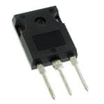
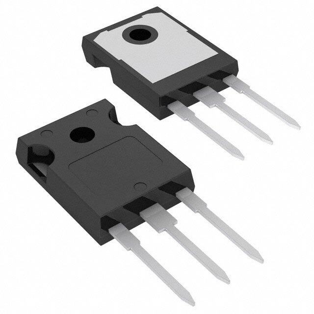
ICGOO电子元器件商城为您提供MJH6284G由ON Semiconductor设计生产,在icgoo商城现货销售,并且可以通过原厂、代理商等渠道进行代购。 MJH6284G价格参考¥28.95-¥32.82。ON SemiconductorMJH6284G封装/规格:晶体管 - 双极 (BJT) - 单, 双极 (BJT) 晶体管 NPN - 达林顿 100V 20A 4MHz 160W 通孔 TO-247。您可以下载MJH6284G参考资料、Datasheet数据手册功能说明书,资料中有MJH6284G 详细功能的应用电路图电压和使用方法及教程。
MJH6284G 是一款由 ON Semiconductor(安森美半导体)生产的双极型晶体管(BJT),属于 NPN 型晶体管。它具有高电流增益、高频率特性和良好的开关性能,因此广泛应用于各种功率放大和开关电路中。以下是 MJH6284G 的主要应用场景:

1. 功率放大器
   MJH6284G 适合用于音频功率放大器和其他需要高增益和大电流输出的功率放大应用。其高电流承载能力和高频特性使其能够在音频设备(如扬声器驱动器)中提供高质量的信号放大。

2. 开关电路
   该晶体管可以作为电子开关使用,在继电器驱动、电机控制或 LED 驱动等场景中发挥重要作用。它的快速开关能力和高耐压值(集电极-发射极击穿电压可达 120V)确保了在这些应用中的可靠运行。

3. 电源管理
   MJH6284G 可用于 DC-DC 转换器、线性稳压器等电源管理电路中,实现高效的电压调节或电流控制。其低饱和电压特性有助于减少功耗并提高效率。

4. 工业自动化
   在工业控制系统中,MJH6284G 可用于驱动电磁阀、步进电机或其他执行机构。它的高电流处理能力(最大集电极电流为 5A)能够满足大多数工业负载的需求。

5. 通信设备
   由于 MJH6284G 支持较高的工作频率(过渡频率 fT 典型值为 250MHz),它也可以用于射频(RF)前端模块、信号调制解调电路以及数据传输相关设备中。

6. 汽车电子
   在汽车领域,该晶体管可用于车灯控制、风扇电机驱动或车载音响系统等场合。其坚固的设计和宽温度范围(-55°C 至 +150°C)适应了汽车环境下的严苛条件。

总结来说,MJH6284G 凭借其出色的电气性能和稳定性,适用于需要高性能功率放大与开关功能的各种电子设备及系统中。选择具体应用时需结合实际需求考虑散热设计和外围电路匹配等因素。
| 参数 | 数值 |
| 产品目录 | |
| 描述 | TRANS DARL NPN 20A 100V TO247达林顿晶体管 20A 100V Bipolar Power NPN |
| 产品分类 | 晶体管(BJT) - 单路分离式半导体 |
| 品牌 | ON Semiconductor |
| 产品手册 | |
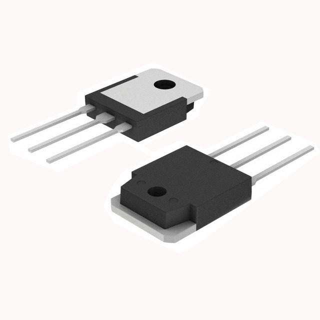
| 产品图片 |
|
| rohs | 符合RoHS无铅 / 符合限制有害物质指令(RoHS)规范要求 |
| 产品系列 | 晶体管,达林顿晶体管,ON Semiconductor MJH6284G- |
| 数据手册 | |
| 产品型号 | MJH6284G |
| PCN封装 | |
| 不同 Ib、Ic时的 Vce饱和值(最大值) | 3V @ 200mA,20A |
| 不同 Ic、Vce 时的DC电流增益(hFE)(最小值) | 750 @ 10A,3V |
| 产品目录页面 | |
| 产品种类 | 达林顿晶体管 |
| 供应商器件封装 | TO-247 |
| 其它名称 | MJH6284GOS |
| 功率-最大值 | 160W |
| 功率耗散 | 160 W |
| 包装 | 管件 |
| 发射极-基极电压VEBO | 5 V |
| 商标 | ON Semiconductor |
| 安装类型 | 通孔 |
| 安装风格 | Through Hole |
| 封装 | Tube |
| 封装/外壳 | TO-247-3 |
| 封装/箱体 | TO-247 |
| 工厂包装数量 | 30 |
| 晶体管极性 | NPN |
| 晶体管类型 | NPN - 达林顿 |
| 最大工作温度 | + 150 C |
| 最大直流电集电极电流 | 20 A |
| 最大集电极截止电流 | 1000 uA |
| 最小工作温度 | - 65 C |
| 标准包装 | 30 |
| 电压-集射极击穿(最大值) | 100V |
| 电流-集电极(Ic)(最大值) | 20A |
| 电流-集电极截止(最大值) | 1mA |
| 直流集电极/BaseGainhfeMin | 100, 750 |
| 系列 | MJH6284 |
| 配置 | Single |
| 集电极—发射极最大电压VCEO | 100 V |
| 集电极—基极电压VCBO | 100 V |
| 集电极连续电流 | 20 A |
| 频率-跃迁 | 4MHz |


PDF Datasheet 数据手册内容提取
MJH6284(cid:2)(NPN), MJH6287(cid:2)(PNP) Darlington Complementary Silicon Power Transistors These devices are designed for general−purpose amplifier and low−speed switching motor control applications. http://onsemi.com Features • DARLINGTON 20 AMPERE Similar to the Popular NPN 2N6284 and the PNP 2N6287 • Rugged RBSOA Characteristics COMPLEMENTARY SILICON • Monolithic Construction with Built−in Collector−Emitter Diode POWER TRANSISTORS • These are Pb−Free Devices* 100 VOLTS, 160 WATTS MAXIMUM RATINGS Rating Symbol Max Unit Collector−Emitter Voltage VCEO 100 Vdc Collector−Base Voltage VCB 100 Vdc Emitter−Base Voltage VEB 5.0 Vdc Collector Current − Continuous IC 20 Adc − Peak 40 Base Current IB 0.5 Adc Total Device Dissipation @ TC = 25(cid:2)C PD 160 W Derate above 25(cid:2)C 1.28 W/(cid:2)C SOT−93 Operating and Storage Junction TJ, Tstg –(cid:2)65 to +(cid:2)150 (cid:2)C (TO−218) Temperature Range CASE 340D THERMAL CHARACTERISTICS Characteristic Symbol Max Unit Thermal Resistance, Junction−to−Case R(cid:2)JC 0.78 (cid:2)C/W Stresses exceeding Maximum Ratings may damage the device. Maximum Ratings are stress ratings only. Functional operation above the Recommended Operating Conditions is not implied. Extended exposure to stresses above the Recommended Operating Conditions may affect device reliability. 160 TO−247 CASE 340L 140 S) STYLE 3 T AT 120 W N ( 100 NOTE: Effective June 2012 this device will O be available only in the TO−247 TI PA 80 package. Reference FPCN# 16827. SI S DI 60 R E OW 40 ORDERING INFORMATION P P, D 20 Sdiemee dnestiaoinlesd s oercdteiornin go na npda gseh ip2p oinf gth inisf odramtaa tsiohne ient .the package 0 0 25 50 75 100 125 150 175 200 TC, CASE TEMPERATURE (°C) Figure 1. Power Derating *For additional information on our Pb−Free strategy and soldering details, please download the ON Semiconductor Soldering and Mounting Techniques Reference Manual, SOLDERRM/D. © Semiconductor Components Industries, LLC, 2012 1 Publication Order Number: May, 2012 − Rev. 7 MJH6284/D
MJH6284 (NPN), MJH6287 (PNP) MARKING DIAGRAMS TO−247 TO−218 MJH628x AYWWG AYWWG MJH628x 1 BASE 3 EMITTER 1 BASE 3 EMITTER 2 COLLECTOR 2 COLLECTOR MJH628x=Device Code x = 4 or 7 A =Assembly Location Y =Year WW =Work Week G =Pb−Free Package ORDERING INFORMATION Device Order Number Package Type Shipping MJH6284G TO−218 30 Units / Rail (Pb−Free) MJH6287G TO−218 30 Units / Rail (Pb−Free) MJH6284G TO−247 30 Units / Rail (Pb−Free) MJH6287G TO−247 30 Units / Rail (Pb−Free) http://onsemi.com 2
MJH6284 (NPN), MJH6287 (PNP) ELECTRICAL CHARACTERISTICS (TC = 25(cid:2)C unless otherwise noted) Characteristic Symbol Min Max Unit OFF CHARACTERISTICS Collector−Emitter Sustaining Voltage (IC = 0.1 Adc, IB = 0) VCEO(sus) 100 − Vdc Collector Cutoff Current (VCE = 50 Vdc, IB = 0) ICEO − 1.0 mAdc Collector Cutoff Current ICEX mAdc (VCE = Rated VCB, VBE(off) = 1.5 Vdc) − 0.5 (VCE = Rated VCB, VBE(off) = 1.5 Vdc, TC = 150(cid:2)C) − 5.0 Emitter Cutoff Current (VBE = 5.0 Vdc, IC = 0) IEBO − 2.0 mAdc ON CHARACTERISTICS (Note 1) DC Current Gain hFE − (IC = 10 Adc, VCE = 3.0 Vdc) 750 18,000 (IC = 20 Adc, VCE = 3.0 Vdc) 100 − Collector−Emitter Saturation Voltage VCE(sat) Vdc (IC = 10 Adc, IB = 40 mAdc) − 2.0 (IC = 20 Adc, IB = 200 mAdc) − 3.0 Base−Emitter On Voltage (IC = 10 Adc, VCE = 3.0 Vdc) VBE(on) − 2.8 Vdc Base−Emitter Saturation Voltage (IC = 20 Adc, IB = 200 mAdc) VBE(sat) − 4.0 Vdc DYNAMIC CHARACTERISTICS Current−Gain Bandwidth Product (IC = 10 Adc, VCE = 3.0 Vdc, f = 1.0 MHz) fT 4.0 − MHz Output Capacitance Cob pF (VCB = 10 Vdc, IE = 0, f = 0.1 MHz) MJH6284 − 400 MJH6287 − 600 Small−Signal Current Gain (IC = 10 Adc, VCE = 3.0 Vdc, f = 1.0 kHz) hfe 300 − − SWITCHING CHARACTERISTICS Typical Resistive Load Symbol NPN PNP Unit Delay Time td 0.1 0.1 (cid:3)s Rise Time VCC = 30 Vdc, IC = 10 Adc tr 0.3 0.3 IB1 = IB2 = 100 mA Storage Time Duty Cycle = 1.0% ts 1.0 1.0 Fall Time tf 3.5 2.0 1. Pulse test: Pulse Width = 300 (cid:3)s, Duty Cycle = 2.0%. RDB1, &M RUCS TV ABREI EFDAS TTO R OEBCTOAVINE RDYE STIYRPEEDS C, eU.Rg.R:ENT LEVELS -V(cid:2)3C0C V MJNHP6N284 MJPHN6P287 (cid:3)1N5825 USED ABOVE IB ≈ 100 mA COLLECTOR COLLECTOR (cid:3)MSD6100 USED BELOW IB ≈ 100 mA RC SCOPE TUT V2 RB APPROX BASE BASE +12 V 0 51 D1 ≈ 8.0 k ≈ 50 V1 APPROX +(cid:2)4.0 V -(cid:2)8.0 V 25 (cid:3)s EMITTER EMITTER tr, tf, ≤ 10 ns for td and tr, D1 is disconnected DUTY CYCLE = 1.0% and V2 = 0 For NPN test circuit reverse diode and voltage polarities. Figure 2. Switching Times Test Circuit Figure 3. Darlington Schematic http://onsemi.com 3
MJH6284 (NPN), MJH6287 (PNP) 1.0 0.7 L D = 0.5 MA 0.5 ERD) HE 0.3 0.2 TZ NT ALI 0.2 EM 0.1 ANSINOR 0.1 0.05 R(cid:2)JC(t) = r(t) R(cid:2)JC P(pk) r(t), EFFECTIVE TRRESISTANCE (0000....00005273 S0I.N0G2LE PULSE0.01 RDPRTJU E(cid:2)C(JpLACUkSD) R=E- T V 0TTIEM.CR7S E8A= °A I ACNPPT/( PpWS tkL1H) Y MOR FA(cid:2)WOJXCNR(t )POWER DUTtY1 CtY2CLE, D = t1/t2 0.01 0.01 0.02 0.03 0.05 0.1 0.2 0.3 0.5 1.0 2.0 3.0 5.0 10 20 30 50 100 200 300 500 1000 t, TIME (ms) Figure 4. Thermal Response FBSOA, FORWARD BIAS SAFE OPERATING AREA 50 0.1 ms S) 20 P M A 10 0.5 ms NT ( 5.0 1.0 ms E R 5.0 ms R dc CU 2.0 R CTO 1.0 TJ = 150°C E L 0.5 L O SECOND BREAKDOWN LIMITED C , C 0.2 BONDING WIRE LIMITED I 0.1 THERMAL LIMITATION @TC = 25°C (SINGLE PULSE) 0.05 2.0 5.0 10 20 50 100 VCE, COLLECTOR-EMITTER VOLTAGE (VOLTS) Figure 5. MJH6284, MJH6287 50 FORWARD BIAS There are two limitations on the power handling ability of PS) a transistor: average junction temperature and second M 40 A breakdown. Safe operating area curves indicate I − V T ( C CE N limits of the transistor that must be observed for reliable E RR 30 operation; i.e., the transistor must not be subjected to greater U DUTY CYCLE = 10% C dissipation than the curves indicate. R O The data of Figure 5 is based on T = 150(cid:2)C; T is CT 20 L = 200 (cid:3)H J(pk) C LLE IC/IB ≥ 100 variable depending on conditions. Second breakdown pulse CO TC = 25°C limits are valid for duty cycles to 10% provided TJ(pk) I, C 10 RVBBEE( o=f f)4 =7 0(cid:4)(cid:2)-(cid:2)5.0 V F(cid:2)ig 1u5re0 (cid:2)4C. A. tT hJi(gphk) c amsea yte mbpee rcaatulcruesla, ttehde rmfraolm li mtihtea tiodnasta w iilnl 0 reduce the power that can be handled to values less than the 0 10 20 30 40 60 80 100 110 limitations imposed by second breakdown. VCE, COLLECTOR-EMITTER VOLTAGE (VOLTS) Figure 6. Maximum RBSOA, Reverse Bias Safe Operating Area http://onsemi.com 4
MJH6284 (NPN), MJH6287 (PNP) NPN PNP 3000 5000 VCE = 3.0 V VCE = 3.0 V 2000 TJ = 150°C 3000 TJ = 150°C N N GAI GAI 2000 25°C T 1000 T N N E E RR 25°C RR U U C C 500 C C 1000 , DE , DE 700 -(cid:2)55°C hF 300 hF 500 -(cid:2)55°C 200 150 300 0.2 0.3 0.5 1.0 2.0 3.0 5.0 7.0 10 20 0.2 0.3 0.5 0.7 1.0 2.0 3.0 5.0 7.0 10 20 IC, COLLECTOR CURRENT (AMPS) IC, COLLECTOR CURRENT (AMPS) Figure 7. DC Current Gain S) 2.8 S) 2.8 T T OL 2.6 OL 2.6 V V GE ( 2.4 TJ = 25°C GE ( 2.4 A A LT 2.2 LT 2.2 O O R V 2.0 R V 2.0 E E TT 1.8 TT 1.8 IC = 15 A MI MI -E 1.6 IC = 15 A -E 1.6 R R TO 1.4 TO 1.4 IC = 10 A C C LE 1.2 IC = 10 A LE 1.2 L L O O , CE 1.0 IC = 5.0 A , CE 1.0 IC = 5.0 A VC 0.8 VC 0.8 1.0 2.03.0 5.0 10 20 30 50 100 200300 500 1000 1.0 2.03.0 5.0 10 20 30 50 100 200300 500 1000 IB, BASE CURRENT (mA) IB, BASE CURRENT (mA) Figure 8. Collector Saturation Region 3.0 3.0 2.5 TJ = 25°C 2.5 TJ = 25°C S) S) T T L L O 2.0 O 2.0 V V E ( E ( VBE(sat) @ IC/IB = 250 G G A A OLT 1.5 VBE @ VCE = 3.0 V OLT 1.5 VBE(on) @ VCE = 3.0 V V V V, V, VBE(sat) @ IC/IB = 250 1.0 1.0 VCE(sat) @ IC/IB = 250 VCE(sat) @ IC/IB = 250 0.5 0.5 0.1 0.2 0.3 0.50.71.0 2.03.0 5.07.010 20 30 0.1 0.2 0.3 0.50.71.0 2.03.0 5.07.010 20 30 IC, COLLECTOR CURRENT (AMPS) IC, COLLECTOR CURRENT (AMPS) Figure 9. “On” Voltages http://onsemi.com 5
MJH6284 (NPN), MJH6287 (PNP) PACKAGE DIMENSIONS SOT−93 (TO−218) CASE 340D−02 ISSUE E C NOTES: 1.DIMENSIONING AND TOLERANCING PER ANSI B Q E Y14.5M, 1982. 2.CONTROLLING DIMENSION: MILLIMETER. MILLIMETERS INCHES DIM MIN MAX MIN MAX U 4 A --- 20.35 --- 0.801 A B 14.70 15.20 0.579 0.598 S L C 4.70 4.90 0.185 0.193 D 1.10 1.30 0.043 0.051 E 1.17 1.37 0.046 0.054 K 1 2 3 G 5.40 5.55 0.213 0.219 H 2.00 3.00 0.079 0.118 J 0.50 0.78 0.020 0.031 K 31.00 REF 1.220 REF L --- 16.20 --- 0.638 Q 4.00 4.10 0.158 0.161 S 17.80 18.20 0.701 0.717 U 4.00 REF 0.157 REF J V 1.75 REF 0.069 D H STYLE 1: PIN 1. BASE V 2. COLLECTOR G 3. EMITTER 4. COLLECTOR TO−247 CASE 340L−02 ISSUE F −T− NOTES: 1. DIMENSIONING AND TOLERANCING PER ANSI C Y14.5M, 1982. −B− 2. CONTROLLING DIMENSION: MILLIMETER. E MILLIMETERS INCHES U L DIM MIN MAX MIN MAX A 20.32 21.08 0.800 8.30 N 4 B 15.75 16.26 0.620 0.640 C 4.70 5.30 0.185 0.209 A −Q− D 1.00 1.40 0.040 0.055 E 1.90 2.60 0.075 0.102 1 2 3 0.63 (0.025) M T B M F 1.65 2.13 0.065 0.084 G 5.45 BSC 0.215 BSC H 1.50 2.49 0.059 0.098 P J 0.40 0.80 0.016 0.031 −Y− K 19.81 20.83 0.780 0.820 L 5.40 6.20 0.212 0.244 K N 4.32 5.49 0.170 0.216 P --- 4.50 --- 0.177 Q 3.55 3.65 0.140 0.144 U 6.15 BSC 0.242 BSC W 2.87 3.12 0.113 0.123 W J F2 PL H STYPLINE 13.:BASE G 2.COLLECTOR D3 PL 3.EMITTER 4.COLLECTOR 0.25 (0.010) M Y Q S http://onsemi.com 6
MJH6284 (NPN), MJH6287 (PNP) ON Semiconductor and are registered trademarks of Semiconductor Components Industries, LLC (SCILLC). SCILLC reserves the right to make changes without further notice to any products herein. SCILLC makes no warranty, representation or guarantee regarding the suitability of its products for any particular purpose, nor does SCILLC assume any liability arising out of the application or use of any product or circuit, and specifically disclaims any and all liability, including without limitation special, consequential or incidental damages. “Typical” parameters which may be provided in SCILLC data sheets and/or specifications can and do vary in different applications and actual performance may vary over time. All operating parameters, including “Typicals” must be validated for each customer application by customer’s technical experts. SCILLC does not convey any license under its patent rights nor the rights of others. SCILLC products are not designed, intended, or authorized for use as components in systems intended for surgical implant into the body, or other applications intended to support or sustain life, or for any other application in which the failure of the SCILLC product could create a situation where personal injury or death may occur. Should Buyer purchase or use SCILLC products for any such unintended or unauthorized application, Buyer shall indemnify and hold SCILLC and its officers, employees, subsidiaries, affiliates, and distributors harmless against all claims, costs, damages, and expenses, and reasonable attorney fees arising out of, directly or indirectly, any claim of personal injury or death associated with such unintended or unauthorized use, even if such claim alleges that SCILLC was negligent regarding the design or manufacture of the part. SCILLC is an Equal Opportunity/Affirmative Action Employer. This literature is subject to all applicable copyright laws and is not for resale in any manner. PUBLICATION ORDERING INFORMATION LITERATURE FULFILLMENT: N. American Technical Support: 800−282−9855 Toll Free ON Semiconductor Website: www.onsemi.com Literature Distribution Center for ON Semiconductor USA/Canada P.O. Box 5163, Denver, Colorado 80217 USA Europe, Middle East and Africa Technical Support: Order Literature: http://www.onsemi.com/orderlit Phone: 303−675−2175 or 800−344−3860 Toll Free USA/Canada Phone: 421 33 790 2910 Fax: 303−675−2176 or 800−344−3867 Toll Free USA/Canada Japan Customer Focus Center For additional information, please contact your local Email: orderlit@onsemi.com Phone: 81−3−5817−1050 Sales Representative http://onsemi.com MJH6284/D 7
Mouser Electronics Authorized Distributor Click to View Pricing, Inventory, Delivery & Lifecycle Information: O N Semiconductor: MJH6284G MJH6287G