
 Datasheet下载
- 型号: SFSKA5M50CF00-R3
- 制造商: Murata
- 库位|库存: xxxx|xxxx
- 要求:
| 数量阶梯 | 香港交货 | 国内含税 |
| +xxxx | $xxxx | ¥xxxx |
查看当月历史价格
查看今年历史价格
SFSKA5M50CF00-R3产品简介:
ICGOO电子元器件商城为您提供SFSKA5M50CF00-R3由Murata设计生产,在icgoo商城现货销售,并且可以通过原厂、代理商等渠道进行代购。 SFSKA5M50CF00-R3价格参考。MurataSFSKA5M50CF00-R3封装/规格:陶瓷滤波器, 。您可以下载SFSKA5M50CF00-R3参考资料、Datasheet数据手册功能说明书,资料中有SFSKA5M50CF00-R3 详细功能的应用电路图电压和使用方法及教程。
Murata Electronics North America生产的型号为SFSKA5M50CF00-R3的陶瓷滤波器,主要应用于高频通信和信号处理领域。这类滤波器因其出色的频率选择性和稳定性,广泛用于各种无线通信设备、射频模块及音频处理系统中。

1. 无线通信设备:该滤波器常用于手机、Wi-Fi路由器、蓝牙设备等无线通信终端中,以确保信号在特定频段内的高效传输,同时抑制其他频段的干扰。它能够有效提高信号质量,减少噪声和杂波,从而提升通信系统的稳定性和可靠性。

2. 射频模块:在射频识别(RFID)、全球定位系统(GPS)以及卫星通信等射频应用中,SFSKA5M50CF00-R3可以精确地筛选出所需的信号频率,确保数据传输的准确性和完整性。此外,它还能够在复杂的电磁环境中保持稳定的性能,适用于工业自动化、物流管理等领域。

3. 音频处理系统:对于音响设备、麦克风和其他音频器材而言,这款滤波器有助于去除不必要的高频噪音,优化音质表现。通过滤除干扰信号,它可以显著提升音频信号的清晰度和保真度,为用户提供更佳的听觉体验。

4. 医疗电子设备:在心电图机、超声波诊断仪等医疗仪器中,陶瓷滤波器可帮助过滤掉环境中的电磁干扰,确保测量结果的准确性。其高可靠性和低功耗特性也使得它非常适合应用于对精度要求极高的医疗场景。

总之,SFSKA5M50CF00-R3陶瓷滤波器凭借其卓越的性能,在众多高科技产品中发挥着不可或缺的作用,为现代通信技术的发展提供了坚实的支持。
| 参数 | 数值 |
| 产品目录 | |
| 描述 | FILTER 5.5MHZ 60KHZ BAND SMD信号调节 5.5MHZ 1000 OHM CHIP Sealed Alumina Bag |
| 产品分类 | |
| 品牌 | Murata Electronics |
| 产品手册 | http://search.murata.co.jp/Ceramy/CatalogAction.do?sHinnm=? &sNHinnm=SFSKA5M50CF00-R3&sNhin_key=SFSKA5M50CF00-R3&sLang=en&sParam=SFSKA |
| 产品图片 |
|
| rohs | 符合RoHS无铅 / 符合限制有害物质指令(RoHS)规范要求 |
| 产品系列 | Murata Electronics SFSKA5M50CF00-R3CERAFIL®, SFSKA |
| mouser_ship_limit | 该产品可能需要其他文件才能进口到中国。 |
| 数据手册 | |
| 产品型号 | SFSKA5M50CF00-R3 |
| 产品 | Ceramic Filters |
| 产品种类 | 信号调节 |
| 其它名称 | 490-8574-1 |
| 包装 | 剪切带 (CT) |
| 商标 | Murata Electronics |
| 商标名 | CERAFIL |
| 大小/尺寸 | 0.335" 长 x 0.150" 宽 (8.50mm x 3.80mm) |
| 安装类型 | 表面贴装 |
| 封装 | Reel |
| 封装/外壳 | 6-SMD,无引线 |
| 工厂包装数量 | 3000 |
| 带宽 | 60kHz |
| 插入损耗 | 6dB |
| 标准包装 | 1 |
| 滤波器类型 | 鉴频器 |
| 阻抗 | 600 Ohms |
| 频率 | 5.5 MHz |
| 高度(最大值) | 0.079"(2.00mm) |


- 商务部:美国ITC正式对集成电路等产品启动337调查
- 曝三星4nm工艺存在良率问题 高通将骁龙8 Gen1或转产台积电
- 太阳诱电将投资9.5亿元在常州建新厂生产MLCC 预计2023年完工
- 英特尔发布欧洲新工厂建设计划 深化IDM 2.0 战略
- 台积电先进制程称霸业界 有大客户加持明年业绩稳了
- 达到5530亿美元!SIA预计今年全球半导体销售额将创下新高
- 英特尔拟将自动驾驶子公司Mobileye上市 估值或超500亿美元
- 三星加码芯片和SET,合并消费电子和移动部门,撤换高东真等 CEO
- 三星电子宣布重大人事变动 还合并消费电子和移动部门
- 海关总署:前11个月进口集成电路产品价值2.52万亿元 增长14.8%
PDF Datasheet 数据手册内容提取
r CERAFIL (Filters/Traps/Discriminators) for Audio/Visual Equipment Cat.No.P50E-6
!Note(cid:129) Please read rating and !CAUTION (for storage, operating, rating, soldering, mounting and handling) in this catalog to prevent smoking and/or burning, etc. (cid:129) This catalog has only typical specifi cations. Therefore, please approve our product specifi cations or transact the approval sheet for product specifi cations before ordering. EU RoHS Compliant (cid:115) All the products in this catalog comply with EU RoHS. (cid:115) EU RoHS is "the European Directive 2011/65/EU on the Restriction of the Use of Certain Hazardous Substances in Electrical and Electronic Equipment." (cid:115) For more details, please refer to our website 'Murata's Approach for EU RoHS' (http://www.murata.com/info/rohs.html).
!Note(cid:129) Please read rating and !CAUTION (for storage, operating, rating, soldering, mounting and handling) in this catalog to prevent smoking and/or burning, etc. (cid:129) This catalog has only typical specifi cations. Therefore, please approve our product specifi cations or transact the approval sheet for product specifi cations before ordering. CONTENTS 1 CERAFILr and "CERAFIL" in this catalog are the trademarks of Murata Manufacturing Co., Ltd. 2 Part Numbering 2 1. CERAFILr 1-1 CERAFILr 10.7MHz 3 1 Small Chip Type SFECF Series 5 2 Chip Type SFECV/SFECK Series 11 4 3 Standard Lead Type SFELF Series 14 4 Low Loss Type SFELF Series 17 5 5 Low Spurious Response Type SFELF Series 20 6 Wide Bandwidth Type SFELF Series 23 6 7 Narrow Bandwidth Type SFELF Series 25 8 For FM-IF Tuners SFELF Series 27 7 Related Data on Lead Type 30 1-2 CERAFILr 2.3-6.5MHz 9 4.5-6.5MHz Chip Type SFSKA Series 31 8 10 2.3-5.7MHz Chip Type SFSKB Series 34 1-3 CERAFILr 455kHz 9 11 Chip Type SFPKA Series 38 12 Lead Type SFPLA/CFWLA Series 40 10 13 For AM Stereo Wide Bandwidth Type SFPLA/CFWLA/CFULA Series 42 SFp Series Temperature Characteristics 44 11 2. Ceramic Trap 14 Ceramic Trap 4.5-6.5MHz Chip Type TPSKA Series 45 3. Ceramic Discriminator 12 15 10.7MHz Ultra Thin Chip Type CDSCB Series 47 Applied IC Reference Table 52 13 Notice 53 Packaging 69 14 Part Number Index 74 15
!Note(cid:129) Please read rating and !CAUTION (for storage, operating, rating, soldering, mounting and handling) in this catalog to prevent smoking and/or burning, etc. (cid:129) This catalog has only typical specifi cations. Therefore, please approve our product specifi cations or transact the approval sheet for product specifi cations before ordering. o Part Numbering CERAFILr for FM (Part Number) SF E LF 10M7 F A A0 -B0 q w e r t y u i qProduct ID yCenter Frequency/Tolerance Product ID Code Center Frequency Tolerance SF Ceramic Filters A Center Frequency mentioned by specification ±30kHz B -30kHz shifted from center frequency of code "A" ±30kHz wOscillation/Number of Elements C +30kHz shifted from center frequency of code "A" ±30kHz Code Oscillation/Number of Elements D -60kHz shifted from center frequency of code "A" ±30kHz E 2 Elements Thickness Expander mode E +60kHz shifted from center frequency of code "A" ±30kHz T 3 Elements Thickness Expander mode H Center Frequency mentioned by specification ±25kHz 2 Elements Thickness Expander mode V -50kHz shifted from center frequency of code "H" ±25kHz V (2nd Harmonic) W +50kHz shifted from center frequency of code "H" ±25kHz 2 Elements Thickness Expander mode K Center Frequency mentioned by specification ±20kHz K (3rd Overtone) Z Combination of A, B, C, D, E — M Combination of A, B, C — eStructure/Size F Nominal Center Frequency — Code Structure/Size 3dB bandwidth of "F" signifies the frequency difference (both + and -) Lp Lead Type from reference frequency, which is nominal center frequency. Cp Chip Type p is "A" or subsequent code, which indicates the structure/size. uSeries Code Series rNominal Center Frequency A0 Two-digit alphanumerics express series Expressed by four-digit alphanumerics. The unit is in hertz (Hz). Decimal point is expressed by capital letter "M" in case of MHz. iPackaging Code Packaging t3dB Bandwidth -B0 Bulk Code 3dB Bandwidth -R0 Embossed Taping ø180mm C 450kHz min -R1 Embossed Taping ø330mm D 350kHz min -A0 1500pcs. /Radial Taping H0=18mm E 330kHz -A1 1000pcs. /Radial Taping H0=18mm F 280kHz Radial taping is applied to lead type and embossed taping to chip type. With non-standard products, two-digit alphanumerics indicating G 230kHz "Individual Specification" are added between "uSeries" and H 180kHz "iPackaging." J 150kHz K 110kHz L 80kHz M 50kHz N 35kHz 2
!Note(cid:129) Please read rating and !CAUTION (for storage, operating, rating, soldering, mounting and handling) in this catalog to prevent smoking and/or burning, etc. (cid:129) This catalog has only typical specifi cations. Therefore, please approve our product specifi cations or transact the approval sheet for product specifi cations before ordering. CCEERRAAFFIILLrr (Part Number) SF S KA 4M50 CF 00 -R1 q w e r t y u qProduct ID tProduct Specification Code (1) Product ID Code Product Specification Code (1) SF Ceramic Filters BF Tight Bandwidth Type CF Standard Bandwidth Type wOscillation/Numbers of Element DF Broad Bandwidth Type Code Oscillation/Numbers of Element EF Ultra-broad Bandwidth Type S 2 Elements Thickness Shear mode yProduct Specification Code (2) eStructure/Size Code Product Specification Code (2) Code Structure/Size 00 Standard Type Kp Chip Type p is "A" or subsequent code, which indicates the structure/size. uPackaging Code Packaging rNominal Center Frequency -B0 Bulk Expressed by four-digit alphanumerics. The unit is in hertz (Hz). -R1 Embossed Taping ø=330mm Decimal point is expressed by capital letter "M" in case of MHz. With non-standard products, two-digit alphanumerics indicating "Individual Specification" is added between "yProduct Specification Code (2)" and "uPackaging." CERAFILr for AM (Part Number) SF P KA 455K D4A -B0 q w e r t y qProduct ID tProduct Specification Product ID Code Product Specification SF Ceramic Filters Three-digit alphanumerics indicate product D4A CF Ceramic Filters specification of 3dB or 6dB frequency tolerance. ppA indicates standard type. wOscillation/Numbers of Element Code Oscillation/Numbers of Element yPackaging P 4 Elements Area Expansion mode Code Packaging -B0 Bulk eStructure/Size -R0 Embossed Taping (ø180mm) Code Structure/Size -R1 Embossed Taping (ø330mm) Lp Lead Type -M0 Magazine Cassette Cp/Kp Chip Type Radial taping is applied to lead type and embossed taping to chip type. p is "A" or subsequent code, which indicates the structure/size. It With non-standard products, three-digit alphanumerics indicating "Individual Specification" is added between "tProduct Specification" varies depending on vibration mode and number of elements. and "yPackaging." rNominal Center Frequency Expressed by four-digit alphanumerics. The unit is in hertz (Hz). Capital letter "K" following three figures expresses the unit of "kHz." 3
!Note(cid:129) Please read rating and !CAUTION (for storage, operating, rating, soldering, mounting and handling) in this catalog to prevent smoking and/or burning, etc. (cid:129) This catalog has only typical specifi cations. Therefore, please approve our product specifi cations or transact the approval sheet for product specifi cations before ordering. Ceramic Traps (Part Number) TP S KA 4M00 B 00 -R0 q w e r t y u qProduct ID tProduct Specification Code (1) Product ID Code Product Specification (1) TP Ceramic Traps B Broad bandwidth Type C Low capacitance Type wFunction Code Function yProduct Specification Code (2) S Single Traps Code Product Specification (2) 00 Standard Type eStructure/Size Code Structure/Size uPackaging Kp Chip Type Code Packaging p is "A" or subsequent code, which indicates the structure/size. -B0 Bulk -R1 Embossed Taping ø=330mm rNominal Center Frequency With non-standard products, three-digit alphanumerics indicating Expressed by four-digit alphanumerics. The unit is in hertz (Hz). "Individual Specification" is added between "yProduct Specification Decimal point is expressed by capital letter "M" in case of MHz. Code (2)" and "uPackaging." Discriminators for FM (Part Number) CD A LF 10M7 G A 001 -B0 q w e r t y u i qProduct ID yCenter Frequency/Tolerance Product ID Code Center Frequency Tolerance CD Discriminators A Center Frequency mentioned by specification ±30kHz B -30kHz shifted from center frequency of code "A" ±30kHz wOscillation C +30kHz shifted from center frequency of code "A" ±30kHz Code Oscillation D -60kHz shifted from center frequency of code "A" ±30kHz A Thickness Expander mode E +60kHz shifted from center frequency of code "A" ±30kHz S Thickness Shear mode H Center Frequency mentioned by specification ±25kHz V -50kHz shifted from center frequency of code "H" ±25kHz eStructure/Size W +50kHz shifted from center frequency of code "H" ±25kHz Code Structure/Size K Center Frequency mentioned by specification ±20kHz Lp Lead Type Z Combination of A, B, C, D, E — Cp Chip Type M Combination of A, B, C — p is "A" or subsequent code, which indicates the structure/size. F Nominal Center Frequency — 3dB bandwidth of "F" signifies the frequency difference (both + and -) rNominal Center Frequency from reference frequency, which is nominal center frequency. Expressed by four-digit alphanumerics. The unit is in hertz (Hz). Decimal point is expressed by capital letter "M" in case of MHz. uIC Code IC tSeries 001 Applicable IC Control Code Code Series G Two-digit alphanumerics express series iPackaging Code Packaging -B0 Bulk -A0 Radial Taping H0=18mm -R0 Embossed Taping ø=180mm -R1 Embossed Taping ø=330mm Radial taping is applied to lead type and embossed taping to chip type. With non-standard products, an alphanumerics indicating "Individual Specification" is added between "uIC" and "iPackaging." 4
!Note• Please read rating and !CAUTION (for storage, operating, rating, soldering, mounting and handling) in this catalog to prevent smoking and/or burning, etc. • This catalog has only typical specifi cations. Therefore, please approve our product specifi cations or transact the approval sheet for product specifi cations before ordering. r r CERAFIL (CERAFIL 10.7MHz) for Audio/Visual Equipment 1 Small Chip Type SFECF Series 3.45±0.2 1.3±0.1 SFECF10M7 series for FM receivers are small, high-performance and super thin (1.4mm max.) fi lters. Imnaprukte erlectrode 3.1±0.2 The piezoelectric element is sandwiched by the ceramic 0 to 0.4(0.6)(0.6)(0.6)0 to 0.4 substrate. They have 1.4mm max. thickness and a small mounting area (3.45x3.1mm). SFECF series and (1.28)(1.28) CDSCB series (MHz Discriminator) enable customers to 0.3 min.0.3 min. make VICS/RKE/TPMS set very thin and small. 0.65±0.30.7±0.3 0.65±0.3 c1. TFheea fit ultererss are mountable by automatic placers. 0.85±0.30.85±0.3 ((16(1)).28)(((521)).28(()43)) 0.75±0.3 ((23( )) (((( 5416 ))))):::::: GNIOERnIoerupAo ftucepJuto runMentdnnocenecthtiloyn Code 2. They are slim, at only 1.4mm max. thickness, and 0 to 0.35 0 to 0.35 (in mm) have a small mounting area (3.45x3.1mm) enabling fl exible PCB design. 3. Various bandwidths are available. Select a suitable type in accordance with the desired selectivity. 4. Operating Temperature Range: -20 to +80°C (Standard Type) -40 to +85°C (High-reliability Type) Storage Temperature Range: -40 to +85°C (Standard Type) -55 to +85°C (High-reliability Type) Standard Type Center Nominal Center 3dB Attenuation Insertion Loss Ripple Spurious Spurious Input/Output Part Number Frequency Frequency (fn) Bandwidth Attenuation Attenuation Impedance (fo) (MHz) (MHz) (kHz) (kHz) (dB) (dB) (1) (dB) (2) (dB) (ohm) 10.700 30 min. 30 min. SFECF10M7HA00-R0 - 180 ±40kHz 470 max. 4.0±2.0dB 1.0 max. 330 ±30kHz [within 9MHz to fo] [within fo to 12MHz] 8.0max. 30 min. 25 min. SFECF10M7HF00-R0 - 10.700 fn±25 min. 510 max. 1.0 max. 330 [at fn] [within 9MHz to fn] [within fn to 12MHz] 10.700 30 min. 30 min. SFECF10M7GA00-R0 - 230 ±50kHz 510 max. 3.5±2.0dB 1.0 max. 330 ±30kHz [within 9MHz to fo] [within fo to 12MHz] 8.0max. 30 min. 25 min. SFECF10M7GF00-R0 - 10.700 fn±45 min. 560 max. 1.0 max. 330 [at fn] [within 9MHz to fn] [within fn to 12MHz] 10.700 30 min. 30 min. SFECF10M7FA00-R0 - 280 ±50kHz 590 max. 3.0±2.0dB 1.0 max. 330 ±30kHz [within 9MHz to fo] [within fo to 12MHz] 7.0max. 30 min. 25 min. SFECF10M7FF00-R0 - 10.700 fn±65 min. 620 max. 1.0 max. 330 [at fn] [within 9MHz to fn] [within fn to 12MHz] 10.700 30 min. 30 min. SFECF10M7EA00-R0 - 330 ±50kHz 700 max. 3.0±2.0dB 1.0 max. 330 ±30kHz [within 9MHz to fo] [within fo to 12MHz] 10.700 35 min. 25 min. SFECF10M7DA0001-R0 - 420 min. 950 max. 3.0±2.0dB 3.0 max. 330 ±30kHz [within 9MHz to fo] [within fo to 12MHz] 6.0max. 20 min. 20 min. SFECF10M7DF00-R0 - 10.700 fn±150 min. 990 max. 3.0 max. 330 [at fn] [within 9MHz to fn] [within fn to 12MHz] Area of Attenuation: [within 20dB] Area of Insertion Loss: at minimum loss point Area of Ripple: within 3dB B.W. Center frequency (fo) defi ned by the center of 3dB bandwidth. For safety purposes, connect the output of fi lters to the IF amplifi er through a D.C. blocking capacitor. Avoid applying a direct current to the output of ceramic fi lters. The order quantity should be an integral multiple of the "Minimum Quantity" shown in the package page. 5
!Note• Please read rating and !CAUTION (for storage, operating, rating, soldering, mounting and handling) in this catalog to prevent smoking and/or burning, etc. • This catalog has only typical specifi cations. Therefore, please approve our product specifi cations or transact the approval sheet for product specifi cations before ordering. High-Reliability Type 1 Center Nominal Center 3dB Attenuation Insertion Loss Ripple Spurious Spurious Input/Output Part Number Frequency Frequency (fn) Bandwidth Attenuation Attenuation Impedance (fo) (MHz) (MHz) (kHz) (kHz) (dB) (dB) (1) (dB) (2) (dB) (ohm) 10.700 30 min. 30 min. SFECF10M7HA00S0-R0 - 180 ±40kHz 470 max. 4.0±2.0dB 1.0 max. 330 ±30kHz [within 9MHz to fo] [within fo to 12MHz] 8.0max. 30 min. 25 min. SFECF10M7HF00S0-R0 - 10.700 fn±25 min. 510 max. 1.0 max. 330 [at fn] [within 9MHz to fn] [within fn to 12MHz] 10.700 30 min. 30 min. SFECF10M7GA00S0-R0 - 230 ±50kHz 510 max. 3.5±2.0dB 1.0 max. 330 ±30kHz [within 9MHz to fo] [within fo to 12MHz] 8.0max. 30 min. 25 min. SFECF10M7GF00S0-R0 - 10.700 fn±45 min. 560 max. 1.0 max. 330 [at fn] [within 9MHz to fn] [within fn to 12MHz] 10.700 30 min. 30 min. SFECF10M7FA00S0-R0 - 280 ±50kHz 590 max. 3.0±2.0dB 1.0 max. 330 ±30kHz [within 9MHz to fo] [within fo to 12MHz] 7.0max. 30 min. 25 min. SFECF10M7FF00S0-R0 - 10.700 fn±65 min. 630 max. 1.0 max. 330 [at fn] [within 9MHz to fn] [within fn to 12MHz] 10.700 30 min. 30 min. SFECF10M7EA00S0-R0 - 330 ±50kHz 700 max. 3.0±2.0dB 1.0 max. 330 ±30kHz [within 9MHz to fo] [within fo to 12MHz] 6.0max. 20 min. 20 min. SFECF10M7DF00S0-R0 - 10.700 fn±145 min. 990 max. 3.0 max. 330 [at fn] [within 9MHz to fn] [within fn to 12MHz] Area of Attenuation: [within 20dB] Area of Insertion Loss: at minimum loss point Area of Ripple: within 3dB B.W. Center frequency (fo) defi ned by the center of 3dB bandwidth. For safety purposes, connect the output of fi lters to the IF amplifi er through a D.C. blocking capacitor. Avoid applying a direct current to the output of ceramic fi lters. The order quantity should be an integral multiple of the "Minimum Quantity" shown in the package page. c Standard Center Frequency Rank Code CODE 30kHz Step 25kHz Step D 10.64MHz±30kHz 10.650MHz±25kHz B 10.67MHz±30kHz 10.675MHz±25kHz A 10.70MHz±30kHz 10.700MHz±25kHz C 10.73MHz±30kHz 10.725MHz±25kHz E 10.76MHz±30kHz 10.750MHz±25kHz Z Combination A, B, C, D, E M Combination A, B, C c Standard Land Pattern Dimensions c Test Circuit 0.1 0.3 (3) (4) (6) (5) (4)0.1 1.05 R1 (2) (5) 0.3 0.3 0.1 1.40 Rg E1 (1) (6)R2 C2 E2 RVoFltmeter (1) (2) (3)0.1 1.05 S.S.G. 0.1 0.1 (1): Input 0.8 0.6 0.8 0.6 0.8 ((23))(((546)))::: GNOoruo tcpuounntdnection CR2g == 1500 Ω± 2 pRF1 (=I n2c8lu0dΩin ±g5 s%tr a y R c2a p=a 3c3it0aΩnc ±e5 a%nd Input capacitance (2)((51)):: IGnrpouutnd of RF voltmeter) (3)(4): No connection It indicates solder resist land pattern. (in mm) E1: S.S.G. Output Voltage (6): Output 6
!Note(cid:129) Please read rating and !CAUTION (for storage, operating, rating, soldering, mounting and handling) in this catalog to prevent smoking and/or burning, etc. (cid:129) This catalog has only typical specifi cations. Therefore, please approve our product specifi cations or transact the approval sheet for product specifi cations before ordering. c Frequency Characteristics Standard Type 1 SFECF10M7HA00-R0/SFECF10M7HF00-R0 SFECF10M7GA00-R0/SFECF10M7GF00-R0 0 7.0 0 7.0 1 6.0 1 6.0 2 5.0 2 5.0 Attenuation (dB) 43 43..00 G.D.T. (μsec.) Attenuation (dB) 43 43..00 G.D.T. (μsec.) 5 2.0 5 2.0 6 1.0 6 1.0 7 0.0 7 0.0 10.300 10.500 10.700 10.900 11.100 10.300 10.500 10.700 10.900 11.100 Frequency (MHz) Frequency (MHz) SFECF10M7FA00-R0/SFECF10M7FF00-R0 SFECF10M7EA00-R0 0 7.0 0 7.0 1 6.0 1 6.0 2 5.0 2 5.0 Attenuation (dB) 43 43..00 G.D.T. (μsec.) Attenuation (dB) 43 43..00 G.D.T. (μsec.) 5 2.0 5 2.0 6 1.0 6 1.0 7 0.0 7 0.0 10.300 10.500 10.700 10.900 11.100 10.300 10.500 10.700 10.900 11.100 Frequency (MHz) Frequency (MHz) SFECF10M7DA0001-R0 SFECF10M7DF00-R0 0 7.0 0 7.0 1 6.0 1 6.0 2 5.0 2 5.0 Attenuation (dB) 43 43..00 G.D.T. (μsec.) Attenuation (dB) 43 43..00 G.D.T. (μsec.) 5 2.0 5 2.0 6 1.0 6 1.0 7 0.0 7 0.0 10.300 10.500 10.700 10.900 11.100 10.300 10.500 10.700 10.900 11.100 Frequency (MHz) Frequency (MHz) 7
!Note(cid:129) Please read rating and !CAUTION (for storage, operating, rating, soldering, mounting and handling) in this catalog to prevent smoking and/or burning, etc. (cid:129) This catalog has only typical specifi cations. Therefore, please approve our product specifi cations or transact the approval sheet for product specifi cations before ordering. c Frequency Characteristics High-reliability Type 1 SFECF10M7HA00S0-R0/SFECF10M7HF00S0-R0 SFECF10M7GA00S0-R0/SFECF10M7GF00S0-R0 0 7.0 0 7.0 1 6.0 1 6.0 2 5.0 2 5.0 Attenuation (dB) 43 43..00 G.D.T. (μsec.) Attenuation (dB) 43 43..00 G.D.T. (μsec.) 5 2.0 5 2.0 6 1.0 6 1.0 7 0.0 7 0.0 10.300 10.500 10.700 10.900 11.100 10.300 10.500 10.700 10.900 11.100 Frequency (MHz) Frequency (MHz) SFECF10M7FA00S0-R0/SFECF10M7FF00S0-R0 SFECF10M7EA00S0-R0 0 7.0 0 7.0 1 6.0 1 6.0 2 5.0 2 5.0 Attenuation (dB) 43 43..00 G.D.T. (μsec.) Attenuation (dB) 43 43..00 G.D.T. (μsec.) 5 2.0 5 2.0 6 1.0 6 1.0 7 0.0 7 0.0 10.300 10.500 10.700 10.900 11.100 10.300 10.500 10.700 10.900 11.100 Frequency (MHz) Frequency (MHz) SFECF10M7DF00S0-R0 0 7.0 1 6.0 2 5.0 Attenuation (dB) 43 43..00 G.D.T. (μsec.) 5 2.0 6 1.0 7 0.0 10.300 10.500 10.700 10.900 11.100 Frequency (MHz) 8
!Note(cid:129) Please read rating and !CAUTION (for storage, operating, rating, soldering, mounting and handling) in this catalog to prevent smoking and/or burning, etc. (cid:129) This catalog has only typical specifi cations. Therefore, please approve our product specifi cations or transact the approval sheet for product specifi cations before ordering. c Frequency Characteristics (Spurious) Standard Type 1 SFECF10M7HA00-R0/SFECF10M7HF00-R0 SFECF10M7GA00-R0/SFECF10M7GF00-R0 0 0 10 10 20 20 B) B) Attenuation (d3400 Attenuation (d3400 50 50 60 60 70 70 8.700 9.700 10.700 11.700 12.700 8.700 9.700 10.700 11.700 12.700 Frequency (MHz) Frequency (MHz) SFECF10M7FA00-R0/SFECF10M7FF00-R0 SFECF10M7EA00-R0 0 0 10 10 20 20 Attenuation (dB)3400 Attenuation (dB)3400 50 50 60 60 70 70 8.700 9.700 10.700 11.700 12.700 8.700 9.700 10.700 11.700 12.700 Frequency (MHz) Frequency (MHz) SFECF10M7DA0001-R0/SFECF10M7DF00-R0 0 10 20 B) Attenuation (d3400 50 60 70 8.700 9.700 10.700 11.700 12.700 Frequency (MHz) 9
!Note(cid:129) Please read rating and !CAUTION (for storage, operating, rating, soldering, mounting and handling) in this catalog to prevent smoking and/or burning, etc. (cid:129) This catalog has only typical specifi cations. Therefore, please approve our product specifi cations or transact the approval sheet for product specifi cations before ordering. c Frequency Characteristics (Spurious) High-reliability Type 1 SFECF10M7HA00S0-R0/SFECF10M7HF00S0-R0 SFECF10M7GA00S0-R0/SFECF10M7GF00S0-R0 0 0 10 10 20 20 B) B) Attenuation (d3400 Attenuation (d3400 50 50 60 60 70 70 8.700 9.700 10.700 11.700 12.700 8.700 9.700 10.700 11.700 12.700 Frequency (MHz) Frequency (MHz) SFECF10M7FA00S0-R0/SFECF10M7FF00S0-R0 SFECF10M7EA00S0-R0 0 0 10 10 20 20 Attenuation (dB)3400 Attenuation (dB)3400 50 50 60 60 70 70 8.700 9.700 10.700 11.700 12.700 8.700 9.700 10.700 11.700 12.700 Frequency (MHz) Frequency (MHz) SFECF10M7DF00S0-R0 0 10 20 B) Attenuation (d3400 50 60 70 8.700 9.700 10.700 11.700 12.700 Frequency (MHz) 10
!Note(cid:129) Please read rating and !CAUTION (for storage, operating, rating, soldering, mounting and handling) in this catalog to prevent smoking and/or burning, etc. (cid:129) This catalog has only typical specifi cations. Therefore, please approve our product specifi cations or transact the approval sheet for product specifi cations before ordering. r r CERAFIL (CERAFIL 10.7MHz) for Audio/Visual Equipment Chip Type SFECV/SFECK Series 2 6.9±0.3 4.05±0.4 SFECV/SFECK10M7 series for FM receivers are monolithic 1.2±0.5 1.2±0.3 1.2±0.5 1.5±0.2 type ceramic fi lters that utilize the thickness expander mcuosdtoem oef rpsi etoz omealekcetr aicn c AerMa/mFiMcs s. eStF vEeCryV t hsienr,i easn de nita cbalen be 2.9±0.3 ∗∗ ∗ useful to the total chip circuit. (3) (2) (1) c1. TFheea ptuierzeoselectric element is sandwiched by heat 1.5±0.2 (1) :: IMnpaurkt in g (2) : Ground resistant substrate, thus it has excellent mechanical 1.0±0.5 1.0±0.5 1.0±0.5 (3) : Output strength, and it is suitable for automatic mounting. ∗∗ : EIAJ Monthly Code ∗∗ : Center Frequency Rank Code (in mm) 2. Various bandwidths are available. Select a suitable type in accordance with the desired selectivity. 3. Operating Temperature Range: -20 to +80°C (Standard Type) -40 to +85°C (High-reliability Type) Storage Temperature Range: -40 to +85°C (Standard Type) -55 to +85°C (High-reliability Type) c Applications 1. Small, thin radios 2. Automotive radios 3. Headphone stereos Standard Type Center 3dB Attenuation Insertion Loss Ripple Spurious Spurious Input/Output Part Number Frequency Bandwidth Attenuation Attenuation Impedance (fo) (MHz) (kHz) (kHz) (dB) (dB) (1) (dB) (2) (dB) (ohm) 15.000 30 min. 30 min. SFECV15M0EQ0001-R0 300 min. 750 max. 7.0max. 1.0 max. 330 ±50kHz [within 14MHz to fo] [within fo to 16MHz] 10.700 35 min. 35 min. SFECV10M7KA00-R0 110 ±30kHz 320 max. 6.0±2.0dB 1.0 max. 330 ±30kHz [within 9MHz to fo] [within fo to 12MHz] 10.700 35 min. 35 min. SFECV10M7JA00-R0 150 ±40kHz 380 max. 5.5±2.0dB 1.0 max. 330 ±30kHz [within 9MHz to fo] [within fo to 12MHz] Area of Attenuation: [within 20dB] Area of Insertion Loss: at minimum loss point Center frequency (fo) defi ned by the center of 3dB bandwidth. For safety purposes, connect the output of fi lters to the IF amplifi er through a D.C. blocking capacitor. Avoid applying a direct current to the output of ceramic fi lters. The order quantity should be an integral multiple of the "Minimum Quantity" shown in the package page. High-Reliability Type Center 3dB Attenuation Insertion Loss Ripple Spurious Spurious Input/Output Part Number Frequency Bandwidth Attenuation Attenuation Impedance (fo) (MHz) (kHz) (kHz) (dB) (dB) (1) (dB) (2) (dB) (ohm) 10.700 35 min. 35 min. SFECK10M7KA00S0-R0 110 ±30kHz 320 max. 6.0±2.0dB 1.0 max. 330 ±30kHz [within 9MHz to fo] [within fo to 12MHz] 10.700 35 min. 35 min. SFECK10M7JA00S0-R0 150 ±40kHz 380 max. 5.5±2.0dB 1.0 max. 330 ±30kHz [within 9MHz to fo] [within fo to 12MHz] Area of Attenuation: [within 20dB] Area of Insertion Loss: at minimum loss point Center frequency (fo) defi ned by the center of 3dB bandwidth. For safety purposes, connect the output of fi lters to the IF amplifi er through a D.C. blocking capacitor. Avoid applying a direct current to the output of ceramic fi lters. The order quantity should be an integral multiple of the "Minimum Quantity" shown in the package page. 11
!Note(cid:129) Please read rating and !CAUTION (for storage, operating, rating, soldering, mounting and handling) in this catalog to prevent smoking and/or burning, etc. (cid:129) This catalog has only typical specifi cations. Therefore, please approve our product specifi cations or transact the approval sheet for product specifi cations before ordering. c Standard Center Frequency Rank Code CODE 30kHz Step 25kHz Step D 10.64MHz±30kHz 10.650MHz±25kHz B 10.67MHz±30kHz 10.675MHz±25kHz 2 A 10.70MHz±30kHz 10.700MHz±25kHz C 10.73MHz±30kHz 10.725MHz±25kHz E 10.76MHz±30kHz 10.750MHz±25kHz Z Combination A, B, C, D, E M Combination A, B, C c Standard Land Pattern Dimensions c Test Circuit 1.2 1.2 1.2 R1 (1) (3) Rg (2) 4.0 E1 R2 C2 E2 RVoFltmeter S.S.G. =-10dBm 1.65 1.65 2.85 2.85 Rg = 50Ω R1 = 280Ω ±5% R2 = 330Ω ±5% (1) : Input C2 = 10 ± 2 pF (Including stray capacitance and Input capacitance (2) : Ground of RF voltmeter) (3) : Output Land (in mm) E1 : S.S.G. Output Voltage c Frequency Characteristics Standard Type SFECV15M0EQ0001-R0 SFECV10M7KA00-R0 0 10.0 0 7.0 1 6.5 2 8.0 2 6.0 Attenuation (dB) 46 64..00 G.D.T. (μsec.) Attenuation (dB) 43 55..05 G.D.T. (μsec.) 5 4.5 8 2.0 6 4.0 10 0.0 7 3.5 14.700 14.800 14.900 15.000 15.100 15.200 15.300 10.300 10.500 10.700 10.900 11.100 Frequency (MHz) Frequency (MHz) SFECV10M7JA00-R0 0 8.0 1 7.5 2 7.0 Attenuation (dB) 43 66..50 G.D.T. (μsec.) 5 5.5 6 5.0 7 4.5 10.300 10.500 10.700 10.900 11.100 Frequency (MHz) 12
!Note(cid:129) Please read rating and !CAUTION (for storage, operating, rating, soldering, mounting and handling) in this catalog to prevent smoking and/or burning, etc. (cid:129) This catalog has only typical specifi cations. Therefore, please approve our product specifi cations or transact the approval sheet for product specifi cations before ordering. c Frequency Characteristics High-reliability Type SFECK10M7KA00S0-R0 SFECK10M7JA00S0-R0 0 7.0 0 8.0 1 6.5 1 7.5 2 2 6.0 2 7.0 Attenuation (dB) 43 55..05 G.D.T. (μsec.) Attenuation (dB) 43 66..50 G.D.T. (μsec.) 5 4.5 5 5.5 6 4.0 6 5.0 7 3.5 7 4.5 10.300 10.500 10.700 10.900 11.100 10.300 10.500 10.700 10.900 11.100 Frequency (MHz) Frequency (MHz) c Frequency Characteristics (Spurious) Standard Type SFECV15M0EQ0001-R0 SFECV10M7KA00-R0 0 0 10 10 20 20 Attenuation (dB) 543000 Attenuation (dB)4300 50 60 60 70 70 80 8.700 9.700 10.700 11.700 12.700 13.000 14.000 15.000 16.000 17.000 Frequency (MHz) Frequency (MHz) SFECV10M7JA00-R0 0 10 20 B) Attenuation (d4300 50 60 70 8.700 9.700 10.700 11.700 12.700 Frequency (MHz) c Frequency Characteristics (Spurious) High-reliability Type SFECK10M7KA00S0-R0 SFECK10M7JA00S0-R0 0 0 10 10 20 20 Attenuation (dB)4300 Attenuation (dB)4300 50 50 60 60 70 70 8.700 9.700 10.700 11.700 12.700 8.700 9.700 10.700 11.700 12.700 Frequency (MHz) Frequency (MHz) 13
!Note(cid:129) Please read rating and !CAUTION (for storage, operating, rating, soldering, mounting and handling) in this catalog to prevent smoking and/or burning, etc. (cid:129) This catalog has only typical specifi cations. Therefore, please approve our product specifi cations or transact the approval sheet for product specifi cations before ordering. r r CERAFIL (CERAFIL 10.7MHz) for Audio/Visual Equipment Standard Lead Type SFELF Series 7.0±2.0 SFELF10M7 series for FM-receivers are monolithic type 3 ceramic fi lters that use the thickness expander mode M A R K I N G oAfs t hpea rpt ioefz toheele ecntrvicir ocnemraemnitc p.rotection program, the solder CE OI A D J E 7.0±2.0 for terminal plating and terminal-element connection 1.38±0.2 1.7±0.1 inside of the ceramic fi lter contain no lead (Pb). 0.5±0.1 5.0±1.0 c Features 2.5±0.22.5±0.2 1 . Tsthreenseg tmh.iniature fi lters have high mechanical SFELF10M7HA00-B0 0.3±0.1 3.0±1.0 (((123)))( :::in IGO nmrupotmuputu)ntd 2. Low loss, favorable waveform symmetry, and high (3) (2) (1) selectivity 3. Various bandwidths are available for applications 7.0±2.0 in wide to narrow bands. 4. Small dispersion and stable characteristics M A R K I N G 5 . ±C3h0apnpgme/ °inC caet n-t2e0r tfore +q8u0e°nCcy. is typically within CE OI A D J E 7.0±2.0 6. High reliability 1.38±0.2 1.7±0.1 0.5±0.1 5.0±1.0 2.5±0.22.5±0.2 SFELF10M7GA00-B0 0.3±0.1 3.0±1.0 (((123)))( :::in IGO nmrupotmuputu)ntd (3) (2) (1) 7.0±2.0 M A R K I N G CE OI A D J E 7.0±2.0 1.38±0.2 1.7±0.1 0.5±0.1 5.0±1.0 2.5±0.22.5±0.2 SFELF10M7FA00-B0 0.3±0.1 3.0±1.0 (((123)))( :::in IGO nmrupotmuputu)ntd (3) (2) (1) Center 3dB Attenuation Insertion Loss Spurious Spurious Input/Output Part Number Frequency Bandwidth Attenuation Attenuation Impedance (fo) (MHz) (kHz) (kHz) (dB) (1) (dB) (2) (dB) (ohm) 10.700 40 min. 40 min. SFELF10M7HA00-B0 180 ±40kHz 520 max. 7.0max. 330 ±30kHz [within 9MHz to fo] [within fo to 12MHz] 10.700 40 min. 40 min. SFELF10M7GA00-B0 230 ±50kHz 570 max. 4.0±2.0dB 330 ±30kHz [within 9MHz to fo] [within fo to 12MHz] 10.700 30 min. 30 min. SFELF10M7FA00-B0 280 ±50kHz 650 max. 4.0±2.0dB 330 ±30kHz [within 9MHz to fo] [within fo to 12MHz] Area of Attenuation: [within 20dB] Area of Insertion Loss: at minimum loss point Center frequency (fo) defi ned by the center of 3dB bandwidth. For safety purposes, connect the output of fi lters to the IF amplifi er through a D.C. blocking capacitor. Avoid applying a direct current to the output of ceramic fi lters. The order quantity should be an integral multiple of the "Minimum Quantity" shown in the package page. 14
!Note(cid:129) Please read rating and !CAUTION (for storage, operating, rating, soldering, mounting and handling) in this catalog to prevent smoking and/or burning, etc. (cid:129) This catalog has only typical specifi cations. Therefore, please approve our product specifi cations or transact the approval sheet for product specifi cations before ordering. c Standard Center Frequency Rank Code CODE 30kHz Step 25kHz Step Color Code D 10.64MHz±30kHz 10.650MHz±25kHz Black B 10.67MHz±30kHz 10.675MHz±25kHz Blue A 10.70MHz±30kHz 10.700MHz±25kHz Red C 10.73MHz±30kHz 10.725MHz±25kHz Orange E 10.76MHz±30kHz 10.750MHz±25kHz White Z Combination A, B, C, D, E M Combination A, B, C 3 c Test Circuit (1) (2) (3) R1 Rg RF R2 C Voltmeter S.S.G Rg + R1 = R2 = Input and Output Impedance C = 10pF (Including stray capacitance and input capacitance of RF voltmeter.) (1) : Input (2) : Ground (3) : Output c Frequency Characteristics SFELF10M7HA00-B0 SFELF10M7GA00-B0 0 6.5 0 6.0 1 6.0 1 5.5 2 5.5 2 5.0 Attenuation (dB) 43 54..05 G.D.T. (μsec.) Attenuation (dB) 43 44..50 G.D.T. (μsec.) 5 4.0 5 3.5 6 3.5 6 3.0 7 3.0 7 2.5 10.500 10.600 10.700 10.800 10.900 10.500 10.600 10.700 10.800 10.900 Frequency (MHz) Frequency (MHz) SFELF10M7FA00-B0 0 5.5 1 5.0 2 4.5 Attenuation (dB) 43 43..05 G.D.T. (μsec.) 5 3.0 6 2.5 7 2.0 10.500 10.600 10.700 10.800 10.900 Frequency (MHz) 15
!Note(cid:129) Please read rating and !CAUTION (for storage, operating, rating, soldering, mounting and handling) in this catalog to prevent smoking and/or burning, etc. (cid:129) This catalog has only typical specifi cations. Therefore, please approve our product specifi cations or transact the approval sheet for product specifi cations before ordering. c Frequency Characteristics (Spurious) SFELF10M7HA00-B0 SFELF10M7GA00-B0 0 0 10 10 20 20 B) B) 3 Attenuation (d3400 Attenuation (d3400 50 50 60 60 70 70 8.700 9.700 10.700 11.700 12.700 8.700 9.700 10.700 11.700 12.700 Frequency (MHz) Frequency (MHz) SFELF10M7FA00-B0 0 10 20 B) Attenuation (d3400 50 60 70 8.700 9.700 10.700 11.700 12.700 Frequency (MHz) 16
!Note(cid:129) Please read rating and !CAUTION (for storage, operating, rating, soldering, mounting and handling) in this catalog to prevent smoking and/or burning, etc. (cid:129) This catalog has only typical specifi cations. Therefore, please approve our product specifi cations or transact the approval sheet for product specifi cations before ordering. r r CERAFIL (CERAFIL 10.7MHz) for Audio/Visual Equipment Low Loss Type SFELF Series 7.0±2.0 SFELF10M7 series for FM receivers are monolithic type ceramic fi lters that use the thickness expander mode M A R K I N G oAfs t hpea rpt ioefz toheele ecntrvicir ocnemraemnitc p.rotection program, the solder CE OI A D J E 7.0±2.0 for terminal plating and terminal-element connection 1.38±0.2 1.7±0.1 inside of the ceramic fi lter contain no lead (Pb). 0.5±0.1 5.0±1.0 4 c Features 2.5±0.22.5±0.2 1 . Icnosnevretinotnio lnoassl pisro 1d utoc t1s..5 TdhBe lsoew teyrp tehsa anr e useful for SFELF10M7JAA0-B0 0.3±0.1 3.0±1.0 (((123)))( :::in IGO nmrupotmuputu)ntd elevating the sensitivity of sets. (3) (2) (1) 2. Small dispersion and stable characteristics 3. Excellent shape factor of frequency response 7.0±2.0 4. Good waveform symmetry M A R K I N G CE OI A D J E 7.0±2.0 1.38±0.2 1.7±0.1 0.5±0.1 5.0±1.0 2.5±0.22.5±0.2 SFELF10M7HAA0-B0 0.3±0.1 3.0±1.0 (((123)))( :::in IGO nmrupotmuputu)ntd (3) (2) (1) 7.0±2.0 7.0±2.0 M A R K I N G M A R K I N G CE OI A D J E 7.0±2.0 CE OI A D J E 7.0±2.0 1.38±0.2 1.38±0.2 1.7±0.1 1.7±0.1 0.5±0.1 5.0±1.0 0.5±0.1 5.0±1.0 2.5±0.22.5±0.2 2.5±0.22.5±0.2 SFELF10M7GAA0-B0 0.3±0.1 3.0±1.0 (((123)))( :::in IGO nmrupotmuputu)ntd SFELF10M7FAA0-B0 0.3±0.1 3.0±1.0 (((123)))( :::in IGO nmrupotmuputu)ntd (3) (2) (1) (3) (2) (1) Center 3dB Attenuation Insertion Loss Spurious Spurious Input/Output Part Number Frequency Bandwidth Attenuation Attenuation Impedance (fo) (MHz) (kHz) (kHz) (dB) (1) (dB) (2) (dB) (ohm) 10.700 35 min. 35 min. SFELF10M7JAA0-B0 150 ±40kHz 360 max. 4.5±2.0dB 330 ±30kHz [within 9MHz to fo] [within fo to 12MHz] 10.700 35 min. 35 min. SFELF10M7HAA0-B0 180 ±40kHz 470 max. 3.5±1.5dB 330 ±30kHz [within 9MHz to fo] [within fo to 12MHz] 10.700 35 min. 35 min. SFELF10M7GAA0-B0 230 ±50kHz 520 max. 3.0±2.0dB 330 ±30kHz [within 9MHz to fo] [within fo to 12MHz] 10.700 30 min. 30 min. SFELF10M7FAA0-B0 280 ±50kHz 590 max. 2.5±2.0dB 330 ±30kHz [within 9MHz to fo] [within fo to 12MHz] Area of Attenuation: [within 20dB] Area of Insertion Loss: at minimum loss point Center frequency (fo) defi ned by the center of 3dB bandwidth. For safety purposes, connect the output of fi lters to the IF amplifi er through a D.C. blocking capacitor. Avoid applying a direct current to the output of ceramic fi lters. The order quantity should be an integral multiple of the "Minimum Quantity" shown in the package page. 17
!Note(cid:129) Please read rating and !CAUTION (for storage, operating, rating, soldering, mounting and handling) in this catalog to prevent smoking and/or burning, etc. (cid:129) This catalog has only typical specifi cations. Therefore, please approve our product specifi cations or transact the approval sheet for product specifi cations before ordering. c Standard Center Frequency Rank Code CODE 30kHz Step 25kHz Step Color Code D 10.64MHz±30kHz 10.650MHz±25kHz Black B 10.67MHz±30kHz 10.675MHz±25kHz Blue A 10.70MHz±30kHz 10.700MHz±25kHz Red C 10.73MHz±30kHz 10.725MHz±25kHz Orange E 10.76MHz±30kHz 10.750MHz±25kHz White Z Combination A, B, C, D, E M Combination A, B, C c Test Circuit 4 (1) (2) (3) R1 Rg RF R2 C Voltmeter S.S.G Rg + R1 = R2 = Input and Output Impedance C = 10pF (Including stray capacitance and input capacitance of RF voltmeter.) (1) : Input (2) : Ground (3) : Output c Frequency Characteristics SFELF10M7JAA0-B0 SFELF10M7HAA0-B0 0 7.0 0 6.5 1 6.5 1 6.0 2 6.0 2 5.5 Attenuation (dB) 43 55..50 G.D.T. (μsec.) Attenuation (dB) 43 54..05 G.D.T. (μsec.) 5 4.5 5 4.0 6 4.0 6 3.5 7 3.5 7 3.0 10.500 10.600 10.700 10.800 10.900 10.500 10.600 10.700 10.800 10.900 Frequency (MHz) Frequency (MHz) SFELF10M7GAA0-B0 SFELF10M7FAA0-B0 0 6.0 0 5.5 1 5.5 1 5.0 2 5.0 2 4.5 Attenuation (dB) 43 44..50 G.D.T. (μsec.) Attenuation (dB) 43 43..05 G.D.T. (μsec.) 5 3.5 5 3.0 6 3.0 6 2.5 7 2.5 7 2.0 10.500 10.600 10.700 10.800 10.900 10.500 10.600 10.700 10.800 10.900 Frequency (MHz) Frequency (MHz) 18
!Note(cid:129) Please read rating and !CAUTION (for storage, operating, rating, soldering, mounting and handling) in this catalog to prevent smoking and/or burning, etc. (cid:129) This catalog has only typical specifi cations. Therefore, please approve our product specifi cations or transact the approval sheet for product specifi cations before ordering. c Frequency Characteristics (Spurious) SFELF10M7JAA0-B0 SFELF10M7HAA0-B0 0 0 10 10 20 20 B) B) Attenuation (d3400 Attenuation (d3400 50 50 60 60 70 70 4 8.700 9.700 10.700 11.700 12.700 8.700 9.700 10.700 11.700 12.700 Frequency (MHz) Frequency (MHz) SFELF10M7GAA0-B0 SFELF10M7FAA0-B0 0 0 10 10 20 20 B) B) Attenuation (d3400 Attenuation (d3400 50 50 60 60 70 70 8.700 9.700 10.700 11.700 12.700 8.700 9.700 10.700 11.700 12.700 Frequency (MHz) Frequency (MHz) 19
!Note(cid:129) Please read rating and !CAUTION (for storage, operating, rating, soldering, mounting and handling) in this catalog to prevent smoking and/or burning, etc. (cid:129) This catalog has only typical specifi cations. Therefore, please approve our product specifi cations or transact the approval sheet for product specifi cations before ordering. r r CERAFIL (CERAFIL 10.7MHz) for Audio/Visual Equipment Low Spurious Response Type SFELF Series 7.5±2.0 SFELF10M7 series for FM-receivers are monolithic type MARKING ceramic fi lters that use the thickness expander mode of the piezoelectric ceramic. ECIOADJE 7.0±2.0 As part of the environment protection program, the solder 1.38±0.2 for terminal plating and terminal-element connection 1.7±0.1 inside of the ceramic fi lter contain no lead (Pb). 0.5±0.1 5.0±1.0 c Features 2.5±0.22.5±0.2 5 Ttoh setsaen dtyapreds fi hltaevrse. lower spurious response compared SFELF10M7KAB0-B0 0.3±0.1 3.0±1.0 (3) (2) (1) (in mm) 7.5±2.0 7.5±2.0 MARKING MARKING ECIOADJE 7.0±2.0 ECIOADJE 7.0±2.0 1.38±0.2 1.38±0.2 1.7±0.1 1.7±0.1 0.5±0.1 5.0±1.0 0.5±0.1 5.0±1.0 2.5±0.22.5±0.2 2.5±0.22.5±0.2 SFELF10M7JAB0-B0 0.3±0.1 3.0±1.0 SFELF10M7HAB0-B0 0.3±0.1 3.0±1.0 (3) (2) (1) (in mm) (3) (2) (1) (in mm) 7.5±2.0 7.5±2.0 MARKING MARKING ECIOADJE 7.0±2.0 ECIOADJE 7.0±2.0 1.38±0.2 1.38±0.2 1.7±0.1 1.7±0.1 0.5±0.1 5.0±1.0 0.5±0.1 5.0±1.0 2.5±0.22.5±0.2 2.5±0.22.5±0.2 SFELF10M7GAB0-B0 0.3±0.1 3.0±1.0 SFELF10M7FAB0-B0 0.3±0.1 3.0±1.0 (3) (2) (1) (in mm) (3) (2) (1) (in mm) Center 3dB Attenuation Insertion Loss Spurious Spurious Input/Output Part Number Frequency Bandwidth Attenuation Attenuation Impedance (fo) (MHz) (kHz) (kHz) (dB) (1) (dB) (2) (dB) (ohm) 10.700 45/30 min. 30 min. SFELF10M7KAB0-B0 110 ±30kHz 350 max. 7.0±2.0dB 330 ±30kHz [within 9MHz to fo] [within fo to 12MHz] 10.700 45 min. 45 min. SFELF10M7JAB0-B0 150 ±40kHz 380 max. 5.5±2.0dB 330 ±30kHz [within 9MHz to fo] [within fo to 12MHz] 10.700 45 min. 45 min. SFELF10M7HAB0-B0 180 ±40kHz 520 max. 5.0±2.0dB 330 ±30kHz [within 9MHz to fo] [within fo to 12MHz] 10.700 45 min. 45 min. SFELF10M7GAB0-B0 230 ±50kHz 570 max. 3.0±2.0dB 330 ±30kHz [within 9MHz to fo] [within fo to 12MHz] Continued on the following page. 20
!Note• Please read rating and !CAUTION (for storage, operating, rating, soldering, mounting and handling) in this catalog to prevent smoking and/or burning, etc. • This catalog has only typical specifi cations. Therefore, please approve our product specifi cations or transact the approval sheet for product specifi cations before ordering. Continued from the preceding page. Center 3dB Attenuation Insertion Loss Spurious Spurious Input/Output Part Number Frequency Bandwidth Attenuation Attenuation Impedance (fo) (MHz) (kHz) (kHz) (dB) (1) (dB) (2) (dB) (ohm) 10.700 45 min. 45 min. SFELF10M7FAB0-B0 280 ±50kHz 650 max. 3.0±2.0dB 330 ±30kHz [within 9MHz to fo] [within fo to 12MHz] Area of Attenuation: [within 20dB] Area of Insertion Loss: at minimum loss point Center frequency (fo) defi ned by the center of 3dB bandwidth. For safety purposes, connect the output of fi lters to the IF amplifi er through a D.C. blocking capacitor. Avoid applying a direct current to the output of ceramic fi lters. The order quantity should be an integral multiple of the "Minimum Quantity" shown in the package page. c Standard Center Frequency Rank Code CODE 30kHz Step 25kHz Step Color Code D 10.64MHz±30kHz 10.650MHz±25kHz Black B 10.67MHz±30kHz 10.675MHz±25kHz Blue A 10.70MHz±30kHz 10.700MHz±25kHz Red C 10.73MHz±30kHz 10.725MHz±25kHz Orange 5 E 10.76MHz±30kHz 10.750MHz±25kHz White Z Combination A, B, C, D, E M Combination A, B, C c Test Circuit (1) (2) (3) R1 Rg RF R2 C Voltmeter S.S.G Rg + R1 = R2 = Input and Output Impedance C = 10pF (Including stray capacitance and input capacitance of RF voltmeter.) (1) : Input (2) : Ground (3) : Output c Frequency Characteristics SFELF10M7KAB0-B0 SFELF10M7JAB0-B0 0 8.0 0 7.0 1 7.5 1 6.5 2 7.0 2 6.0 Attenuation (dB) 34 66..50 G.D.T. (μsec.) Attenuation (dB) 34 55..50 G.D.T. (μsec.) 5 5.5 5 4.5 6 5.0 6 4.0 7 4.5 7 3.5 10.500 10.600 10.700 10.800 10.900 10.500 10.600 10.700 10.800 10.900 Frequency (MHz) Frequency (MHz) SFELF10M7HAB0-B0 SFELF10M7GAB0-B0 0 6.5 0 6.0 1 6.0 1 5.5 2 5.5 2 5.0 Attenuation (dB) 43 54..05 G.D.T. (μsec.) Attenuation (dB) 43 44..50 G.D.T. (μsec.) 5 4.0 5 3.5 6 3.5 6 3.0 7 3.0 7 2.5 10.500 10.600 10.700 10.800 10.900 10.500 10.600 10.700 10.800 10.900 Frequency (MHz) Frequency (MHz) Continued on the following page. 21
!Note(cid:129) Please read rating and !CAUTION (for storage, operating, rating, soldering, mounting and handling) in this catalog to prevent smoking and/or burning, etc. (cid:129) This catalog has only typical specifi cations. Therefore, please approve our product specifi cations or transact the approval sheet for product specifi cations before ordering. Continued from the preceding page. c Frequency Characteristics SFELF10M7FAB0-B0 0 5.5 1 5.0 2 4.5 Attenuation (dB) 43 43..05 G.D.T. (μsec.) 5 3.0 6 2.5 7 2.0 10.500 10.600 10.700 10.800 10.900 Frequency (MHz) c Frequency Characteristics (Spurious) 5 SFELF10M7KAB0-B0 SFELF10M7JAB0-B0 0 0 10 10 20 20 Attenuation (dB) 3400 Attenuation (dB) 3400 50 50 60 60 70 70 8.700 9.700 10.700 11.700 12.700 8.700 9.700 10.700 11.700 12.700 Frequency (MHz) Frequency (MHz) SFELF10M7HAB0-B0 SFELF10M7GAB0-B0 0 0 10 10 20 20 B) B) Attenuation (d3400 Attenuation (d3400 50 50 60 60 70 70 8.700 9.700 10.700 11.700 12.700 8.700 9.700 10.700 11.700 12.700 Frequency (MHz) Frequency (MHz) SFELF10M7FAB0-B0 0 10 20 B) Attenuation (d3400 50 60 70 8.700 9.700 10.700 11.700 12.700 Frequency (MHz) 22
!Note(cid:129) Please read rating and !CAUTION (for storage, operating, rating, soldering, mounting and handling) in this catalog to prevent smoking and/or burning, etc. (cid:129) This catalog has only typical specifi cations. Therefore, please approve our product specifi cations or transact the approval sheet for product specifi cations before ordering. r r CERAFIL (CERAFIL 10.7MHz) for Audio/Visual Equipment Wide Bandwidth Type SFELF Series 7.0±2.0 SFELF10M7 series for FM-receivers are monolithic type ceramic fi lters that use the thickness expander mode M A R K I N G oAfs t hpea rpt ioefz toheele ecntrvicir ocnemraemnitc p.rotection program, the solder CE OI A D J E 7.0±2.0 for terminal plating and terminal-element connection 1.38±0.2 1.7±0.1 inside of the ceramic fi lter contain no lead (Pb). 0.5±0.1 5.0±1.0 c Features 2.5±0.22.5±0.2 Rcoenavlieznetsio wniadle cre braamndic c fih laterarsc.teristics not obtained by SFELF10M7EA00-B0 0.3±0.1 3.0±1.0 (((123)))( :::in IGO nmrupotmuputu)ntd (3) (2) (1) 7.0±2.0 6 M A R K I N G CE OI A D J E 7.0±2.0 1.38±0.2 1.7±0.1 0.5±0.1 5.0±1.0 2.5±0.22.5±0.2 SFELF10M7DF00-B0 0.3±0.1 3.0±1.0 (((123)))( :::in IGO nmrupotmuputu)ntd (3) (2) (1) Center Nominal Center 3dB Attenuation Insertion Loss Spurious Spurious Input/Output Part Number Frequency Frequency (fn) Bandwidth Attenuation Attenuation Impedance (fo) (MHz) (MHz) (kHz) (kHz) (dB) (1) (dB) (2) (dB) (ohm) 10.700 30 min. 30 min. SFELF10M7EA00-B0 - 330 ±50kHz 680 max. 4.0±2.0dB 330 ±30kHz [within 9MHz to fo] [within fo to 12MHz] 20 min. 20 min. SFELF10M7DF00-B0 - 10.700 fn±175 min. 950 max. 3.0±2.0dB 470 [within 5MHz to fn] [within fn to 15MHz] Area of Attenuation: [within 20dB] Area of Insertion Loss: at minimum loss point Center frequency (fo) defi ned by the center of 3dB bandwidth. For safety purposes, connect the output of fi lters to the IF amplifi er through a D.C. blocking capacitor. Avoid applying a direct current to the output of ceramic fi lters. The order quantity should be an integral multiple of the "Minimum Quantity" shown in the package page. c Standard Center Frequency Rank Code (SFELF10M7EA00-B0) CODE 30kHz Step 25kHz Step Color Code D 10.64MHz±30kHz 10.650MHz±25kHz Black B 10.67MHz±30kHz 10.675MHz±25kHz Blue A 10.70MHz±30kHz 10.700MHz±25kHz Red C 10.73MHz±30kHz 10.725MHz±25kHz Orange E 10.76MHz±30kHz 10.750MHz±25kHz White Z Combination A, B, C, D, E M Combination A, B, C 23
!Note(cid:129) Please read rating and !CAUTION (for storage, operating, rating, soldering, mounting and handling) in this catalog to prevent smoking and/or burning, etc. (cid:129) This catalog has only typical specifi cations. Therefore, please approve our product specifi cations or transact the approval sheet for product specifi cations before ordering. c Test Circuit (1) (2) (3) R1 Rg RF R2 C Voltmeter S.S.G Rg + R1 = R2 = Input and Output Impedance C = 10pF (Including stray capacitance and input capacitance of RF voltmeter.) (1) : Input (2) : Ground (3) : Output c Frequency Characteristics SFELF10M7EA00-B0 SFELF10M7DF00-B0 0 4.5 0 4.5 1 4.0 1 4.0 2 3.5 2 3.5 6 Attenuation (dB) 34 32..05 G.D.T. (μsec.) Attenuation (dB) 43 32..05 G.D.T. (μsec.) 5 2.0 5 2.0 6 1.5 6 1.5 7 1.0 7 1.0 10.300 10.500 10.700 10.900 11.100 10.300 10.500 10.700 10.900 11.100 Frequency (MHz) Frequency (MHz) c Frequency Characteristics (Spurious) SFELF10M7EA00-B0 SFELF10M7DF00-B0 0 0 10 10 20 20 B) B) Attenuation (d 3400 Attenuation (d3400 50 50 60 60 70 70 8.700 9.700 10.700 11.700 12.700 8.700 9.700 10.700 11.700 12.700 Frequency (MHz) Frequency (MHz) 24
!Note(cid:129) Please read rating and !CAUTION (for storage, operating, rating, soldering, mounting and handling) in this catalog to prevent smoking and/or burning, etc. (cid:129) This catalog has only typical specifi cations. Therefore, please approve our product specifi cations or transact the approval sheet for product specifi cations before ordering. r r CERAFIL (CERAFIL 10.7MHz) for Audio/Visual Equipment Narrow Bandwidth Type SFELF Series 7.0±2.0 c Features SFELF10M7LFTA/KAH0 series realizes narrower band M A R K I N G cfi hltearrsa.c Bteerissitdicess ,n lootw o sbptauirnioeuds b ayn cdo tnevmenpteiorantaulr ece ramic CE OI A D J E 7.0±2.0 characteristics are stable. This series is suitable for 1.38±0.2 1.7±0.1 Eneuerodpse satna bclaer n-aaurrdoiow obra AnMd cuhpacroancvteerrissitoicns .u se that 0.5±0.1 5.0±1.0 As part of the environment protection program, the solder 2.5±0.22.5±0.2 finosr itdeerm oifn tahle p claetrianmg iacn fid lt eterr cmoinnatal-ine lenmo elenatd c o(Pnbn)e.ction SFELF10M7LFTA-B0 0.3±0.1 3.0±1.0 (((123)))( :::in IGO nmrupotmuputu)ntd (3) (2) (1) 7.0±2.0 M A R K I N G CE OI A D J E 7.0±2.0 7 1.38±0.2 1.7±0.1 0.5±0.1 5.0±1.0 2.5±0.22.5±0.2 SFELF10M7KAH0-B0 0.3±0.1 3.0±1.0 (((123)))( :::in IGO nmrupotmuputu)ntd (3) (2) (1) Center Nominal Center 3dB Attenuation Insertion Loss Spurious Spurious Input/Output Part Number Frequency Frequency (fn) Bandwidth Attenuation Attenuation Impedance (fo) (MHz) (MHz) (kHz) (kHz) (dB) (1) (dB) (2) (dB) (ohm) 30 min. 30 min. SFELF10M7LFTA-B0 - 10.700 fn±25 min. 280 max. 7.0±2.0dB 330 [within 9MHz to fn] [within fn to 12MHz] 10.700 30 min. 30 min. SFELF10M7KAH0-B0 - 110 ±30kHz 350 max. 7.0±2.0dB 330 ±30kHz [within 9MHz to fo] [within fo to 12MHz] Area of Attenuation: [within 20dB] Area of Insertion Loss: at minimum loss point Center frequency (fo) defi ned by the center of 3dB bandwidth. For safety purposes, connect the output of fi lters to the IF amplifi er through a D.C. blocking capacitor. Avoid applying a direct current to the output of ceramic fi lters. The order quantity should be an integral multiple of the "Minimum Quantity" shown in the package page. c Standard Center Frequency Rank Code (SFELF10M7KAH0-B0) CODE 30kHz Step 25kHz Step Color Code D 10.64MHz±30kHz 10.650MHz±25kHz Black B 10.67MHz±30kHz 10.675MHz±25kHz Blue A 10.70MHz±30kHz 10.700MHz±25kHz Red C 10.73MHz±30kHz 10.725MHz±25kHz Orange E 10.76MHz±30kHz 10.750MHz±25kHz White Z Combination A, B, C, D, E M Combination A, B, C 25
!Note(cid:129) Please read rating and !CAUTION (for storage, operating, rating, soldering, mounting and handling) in this catalog to prevent smoking and/or burning, etc. (cid:129) This catalog has only typical specifi cations. Therefore, please approve our product specifi cations or transact the approval sheet for product specifi cations before ordering. c Test Circuit (1) (2) (3) R1 Rg RF R2 C Voltmeter S.S.G Rg + R1 = R2 = Input and Output Impedance C = 10pF (Including stray capacitance and input capacitance of RF voltmeter.) (1) : Input (2) : Ground (3) : Output c Frequency Characteristics SFELF10M7LFTA-B0 SFELF10M7KAH0-B0 0 12.0 0 8.0 1 11.0 1 7.5 2 10.0 2 7.0 Attenuation (dB) 43 98..00 G.D.T. (μsec.) Attenuation (dB) 34 66..50 G.D.T. (μsec.) 7 5 7.0 5 5.5 6 6.0 6 5.0 7 5.0 7 4.5 10.600 10.650 10.700 10.750 10.800 10.600 10.650 10.700 10.750 10.800 Frequency (MHz) Frequency (MHz) c Frequency Characteristics (Spurious) SFELF10M7LFTA-B0 SFELF10M7KAH0-B0 0 0 10 10 20 20 Attenuation (dB)3400 Attenuation (dB) 3400 50 50 60 60 70 70 8.700 9.700 10.700 11.700 12.700 8.700 9.700 10.700 11.700 12.700 Frequency (MHz) Frequency (MHz) 26
!Note(cid:129) Please read rating and !CAUTION (for storage, operating, rating, soldering, mounting and handling) in this catalog to prevent smoking and/or burning, etc. (cid:129) This catalog has only typical specifi cations. Therefore, please approve our product specifi cations or transact the approval sheet for product specifi cations before ordering. r r CERAFIL (CERAFIL 10.7MHz) for Audio/Visual Equipment For FM-IF Tuners SFELF Series 7.0±2.0 SFELF10M7 series for FM-receivers are monolithic type ceramic fi lters that use the thickness expander mode M A R K I N G oAfs t hpea rpt ioefz toheele ecntrvicir ocnemraemnitc p.rotection program, the solder CE OI A D J E 7.0±2.0 for terminal plating and terminal-element connection 1.38±0.2 1.7±0.1 inside of the ceramic fi lter contain no lead (Pb). 0.5±0.1 5.0±1.0 c Features 2.5±0.22.5±0.2 1 . Lpihttales ed icshpaerrasciotenr iosft iacsm (pGlit.u Dd.e T c.h cahraarcatectreisrtiisctsic as)nd SFELF10M7HA0G-B0 0.3±0.1 3.0±1.0 (((123)))( :::in IGO nmrupotmuputu)ntd 2. The SFELF_G series is based on SFELF_FA00/GA00/ (3) (2) (1) HA00, and it obtains high selectivity with low loss. There is little dispersion of amplitude and GDT 7.0±2.0 characteristics, and low distortion rate can be obtained. M A R K I N G 3. The fl atness of GDT is inspected for all products. CE OI A D J E 7.0±2.0 1.38±0.2 1.7±0.1 0.5±0.1 5.0±1.0 2.5±0.22.5±0.2 8 SFELF10M7GA0G-B0 0.3±0.1 3.0±1.0 (((123)))( :::in IGO nmrupotmuputu)ntd (3) (2) (1) 7.0±2.0 M A R K I N G CE OI A D J E 7.0±2.0 1.38±0.2 1.7±0.1 0.5±0.1 5.0±1.0 2.5±0.22.5±0.2 SFELF10M7FA0G-B0 0.3±0.1 3.0±1.0 (((123)))( :::in IGO nmrupotmuputu)ntd (3) (2) (1) Center 3dB Attenuation Insertion Loss Spurious Spurious GDT Bandwidth Input/Output Part Number Frequency Bandwidth Attenuation Attenuation Impedance (fo) (MHz) (kHz) (kHz) (dB) (1) (dB) (2) (dB) (kHz) (ohm) 10.700 40 min. 40 min. SFELF10M7HA0G-B0 180 ±40kHz 520 max. 7.0max. fo±45min. 330 ±30kHz [within 9MHz to fo] [within fo to 12MHz] 10.700 40 min. 40 min. SFELF10M7GA0G-B0 230 ±50kHz 600 max. 7.0max. fo±60min. 330 ±30kHz [within 9MHz to fo] [within fo to 12MHz] 10.700 30 min. 30 min. SFELF10M7FA0G-B0 280 ±50kHz 650 max. 4.0±2.0dB fo±85min. 330 ±30kHz [within 9MHz to fo] [within fo to 12MHz] Area of Attenuation: [within 20dB] Area of Insertion Loss: at minimum loss point Center frequency (fo) defi ned by the center of 3dB bandwidth. For safety purposes, connect the output of fi lters to the IF amplifi er through a D.C. blocking capacitor. Avoid applying a direct current to the output of ceramic fi lters. The order quantity should be an integral multiple of the "Minimum Quantity" shown in the package page. 27
!Note(cid:129) Please read rating and !CAUTION (for storage, operating, rating, soldering, mounting and handling) in this catalog to prevent smoking and/or burning, etc. (cid:129) This catalog has only typical specifi cations. Therefore, please approve our product specifi cations or transact the approval sheet for product specifi cations before ordering. c Standard Center Frequency Rank Code CODE 30kHz Step 25kHz Step Color Code D 10.64MHz±30kHz 10.650MHz±25kHz Black B 10.67MHz±30kHz 10.675MHz±25kHz Blue A 10.70MHz±30kHz 10.700MHz±25kHz Red C 10.73MHz±30kHz 10.725MHz±25kHz Orange E 10.76MHz±30kHz 10.750MHz±25kHz White Z Combination A, B, C, D, E M Combination A, B, C c Test Circuit (1) (2) (3) R1 Rg RF R2 C Voltmeter S.S.G Rg + R1 = R2 = Input and Output Impedance C = 10pF (Including stray capacitance and input capacitance of RF voltmeter.) (1) : Input (2) : Ground (3) : Output c Frequency Characteristics SFELF10M7HA0G-B0 SFELF10M7GA0G-B0 0 6.5 0 6.0 8 1 6.0 1 5.5 2 5.5 2 5.0 Attenuation (dB) 43 54..05 G.D.T. (μsec.) Attenuation (dB) 43 44..50 G.D.T. (μsec.) 5 4.0 5 3.5 6 3.5 6 3.0 7 3.0 7 2.5 10.400 10.500 10.600 10.700 10.800 10.900 11.000 10.400 10.500 10.600 10.700 10.800 10.900 11.000 Frequency (MHz) Frequency (MHz) SFELF10M7FA0G-B0 0 5.5 1 5.0 2 4.5 Attenuation (dB) 43 43..05 G.D.T. (μsec.) 5 3.0 6 2.5 7 2.0 10.400 10.500 10.600 10.700 10.800 10.900 11.000 Frequency (MHz) 28
!Note(cid:129) Please read rating and !CAUTION (for storage, operating, rating, soldering, mounting and handling) in this catalog to prevent smoking and/or burning, etc. (cid:129) This catalog has only typical specifi cations. Therefore, please approve our product specifi cations or transact the approval sheet for product specifi cations before ordering. c Frequency Characteristics (Spurious) SFELF10M7HA0G-B0 SFELF10M7GA0G-B0 0 0 10 10 20 20 B) B) Attenuation (d3400 Attenuation (d3400 50 50 60 60 70 70 8.700 9.700 10.700 11.700 12.700 8.700 9.700 10.700 11.700 12.700 Frequency (MHz) Frequency (MHz) SFELF10M7FA0G-B0 0 10 20 B) Attenuation (d3400 50 60 70 8.700 9.700 10.700 11.700 12.700 Frequency (MHz) 8 29
!Note(cid:129) Please read rating and !CAUTION (for storage, operating, rating, soldering, mounting and handling) in this catalog to prevent smoking and/or burning, etc. (cid:129) This catalog has only typical specifi cations. Therefore, please approve our product specifi cations or transact the approval sheet for product specifi cations before ordering. CERAFILr 10.7MHz Related Data on Lead Type c Temperature Characteristics SFELF10M7GA00-B0 SFELF10M7HA00-B0 +40 +40 Hz) +20 Center frequency Hz) +20 Center frequency Variation (k ––42000 Variation (k ––42000 –20 0 +20 +40 +60 +80 –20 0 +20 +40 +60 +80 +2 Temperature (°C) +2 Temperature (°C) Variation (dB) +–101 Insertion loss Variation (dB) +–101 Insertion loss –2 –2 –20 0 +20 +40 +60 +80 –20 0 +20 +40 +60 +80 +40 Temperature (°C) +40 Temperature (°C) Variation (kHz) +––4220000 3dB Bandwidth Variation (kHz) +––2420000 3dB Bandwidth –20 0 +20 +40 +60 +80 –20 0 +20 +40 +60 +80 Temperature (°C) Temperature (°C) c Matching Conditions 1. When using ceramic fi lters, it is most important to 3. The SFELF10M7 series are of input/output symmetric match the input/output load to impedance 330 ohm structure so that in theory there is no input/output (SFELF10M7DF00-B0 is 470 ohm). directionality. Actual circuits may use different Waveform symmetry is damaged when reactance is input/output loading conditions (for example, added to the input/output load. mismatched impedance) or capacitance load. In such 2. Two ceramic fi lters directly connected can be used cases, the waveform will be a little changed by the for high selectivity. For reducing waveform direction of the input/output of the ceramic fi lters. variation, it is recommended to input a buffer AMP between ceramic fi lters. c Loaded Resistance and Waveform (Rg+R1=330 ohm) SFELF10M7GA00-B0 Attenuation (dB) 7654321010.5 10.6R21=02.270Ω10.8 10.9 1100000......208642 Group Delay Time (μsec.) Attenuation (dB) 7654321010.5 10.6R2=103.370Ω10.8 10.9 1100000......208642 Group Delay Time (μsec.) Frequency (MHz) Frequency (MHz) Attenuation (dB) 7654321010.5 10.6R21=05.670Ω10.8 10.9 1100000......208642 Group Delay Time (μsec.) Attenuation (dB) 7654321010.5 10.6R21=01.7kΩ10.8 10.9 1100000......208642 Group Delay Time (μsec.) Frequency (MHz) Frequency (MHz) c Loaded Capacitance and Waveform (Rg+R1=R2=330 ohm) SFELF10M7HA00-B0 C=10pF C=33pF Attenuation (dB) 7654321010.5 10.6 10.7 10.8 10.9 1100000......208642 Group Delay Time (μsec.) Attenuation (dB) 7654321010.5 10.6 10.7 10.8 10.9 1100000......208642 Group Delay Time (μsec.) Frequency (MHz) Frequency (MHz) Attenuation (dB) 7654321010.5 10.6C=1506.7pF10.8 10.9 1100000......208642 Group Delay Time (μsec.) Attenuation (dB) 7654321010.5 10.6C=1802.7pF10.8 10.9 1100000......208642 Group Delay Time (μsec.) Frequency (MHz) Frequency (MHz) 30
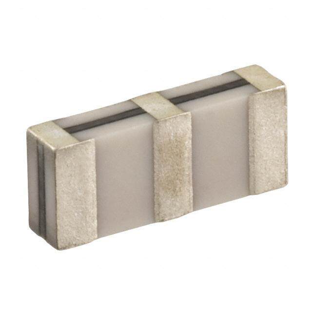
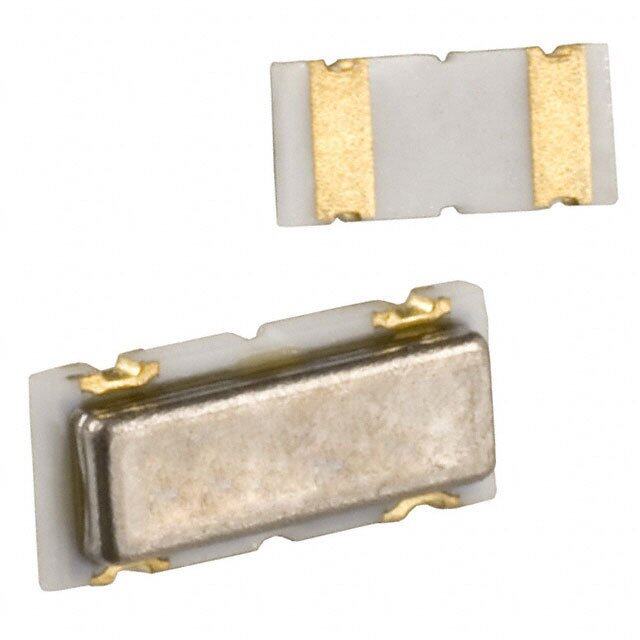
!Note(cid:129) Please read rating and !CAUTION (for storage, operating, rating, soldering, mounting and handling) in this catalog to prevent smoking and/or burning, etc. (cid:129) This catalog has only typical specifi cations. Therefore, please approve our product specifi cations or transact the approval sheet for product specifi cations before ordering. r r CERAFIL (CERAFIL 2.3-6.5MHz) for Audio/Visual Equipment 4.5-6.5MHz Chip Type SFSKA Series SMD ceramic fi lter SFSKA_CF is a small and thin SMD fi lter sealed with a metal cap. Recommended for LCD-TVs, and small and thin tuners. 7.9±0.2 3.0±0.1 1.8±0.2 c Features 0.5±0.1 8.5±0.2 3.8±0.2 1. High attenuation outside bandwidth 0.6±0.2 1.0±0.1 2. Small and thin package 1.3±0.2 3. Refl ow-solderable 0.3±0.1 (1) : Input 1.3±0.2 (2) : Ground (3) : Output (1) (2) (3) (in mm) 2.5±0.2 2.5±0.2 Nominal Center 3dB 20dB Insertion Spurious Spurious Input/Output Part Number Frequency (fn) Bandwidth Bandwidth Loss Attenuation(1) Attenuation(2) Impedance (MHz) (kHz) (kHz) (dB) (dB) (dB) (ohm) 20 min. 15 min. SFSKA4M50CF00-R3 4.500 fn±60 min. 600 max. 6.0 max. 1000 [within 0 to fn] [within fn to 7.0MHz] 25 min. 15 min. SFSKA5M50CF00-R3 5.500 fn±60 min. 600 max. 6.0 max. 600 [within 0 to fn] [within fn to 7.0MHz] 25 min. 15 min. SFSKA6M00CF00-R3 6.000 fn±60 min. 600 max. 6.0 max. 470 [within 0 to fn] [within fn to 7.5MHz] 25 min. 15 min. SFSKA6M50CF00-R3 6.500 fn±60 min. 600 max. 6.0 max. 470 [within 0 to fn] [within fn to 8.5MHz] Area of Insertion Loss: at minimum loss point For safety purposes, connect the output of fi lters to the IF amplifi er through a D.C. blocking capacitor. Avoid applying a direct current to the output of ceramic fi lters. The order quantity should be an integral multiple of the "Minimum Quantity" shown in the package page. 9 c Standard Land Pattern Dimensions c Test Circuit SFSKA4M50CF00-R3 (1) (2) (3) 1.0 1.0 1.0 1.5 1.5 R1 Rg 4.8 E1 R2 C2 E2 RVoFltmeter S.S.G. (in mm) RC12+=R10gp=FR (2I=n1cl0u0d0inΩg ±s5tr%ay, Rcagp=a5c0itΩance and Input capacitance of RF Voltmeter) ((12)) :: IGnrpouutnd E1:S.S.G. Output voltage (3) : Output Continued on the following page. 31
!Note(cid:129) Please read rating and !CAUTION (for storage, operating, rating, soldering, mounting and handling) in this catalog to prevent smoking and/or burning, etc. (cid:129) This catalog has only typical specifi cations. Therefore, please approve our product specifi cations or transact the approval sheet for product specifi cations before ordering. Continued from the preceding page. c Test Circuit SFSKA5M50CF00-R3 SFSKA6M00CF00-R3 (1) (2) (3) (1) (2) (3) R1 R1 Rg Rg RF RF E1 R2 C2 E2 Voltmeter E1 R2 C2 E2 Voltmeter S.S.G. S.S.G. R1+Rg=R2=600Ω ±5%, Rg=50Ω (1) : Input R1+Rg=R2=470Ω ±5%, Rg=50Ω (1) : Input C2=10pF (Including stray capacitance and Input capacitance of RF Voltmeter) (2) : Ground C2=10pF (Including stray capacitance and Input capacitance of RF Voltmeter) (2) : Ground E1: S.S.G. Output voltage (3) : Output E1: S.S.G. Output voltage (3) : Output SFSKA6M50CF00-R3 (1) (2) (3) R1 Rg RF E1 R2 C2 E2 Voltmeter S.S.G. R1+Rg=R2=470Ω ±5%, Rg=50Ω (1) : Input C2=10pF (Including stray capacitance and Input capacitance of RF Voltmeter) (2) : Ground E1: S.S.G. Output voltage (3) : Output c Frequency Characteristics SFSKA4M50CF00-R3 SFSKA5M50CF00-R3 9 0 0 10 10 20 20 B) Attenuation (d 345000 Attenuation (dB) 345000 60 60 70 70 3.5 3.7 3.9 4.1 4.3 4.5 4.7 4.9 5.1 5.3 5.5 4.5 4.7 4.9 5.1 5.3 5.5 5.7 5.9 6.1 6.3 6.5 Frequency (MHz) Frequency (MHz) SFSKA6M00CF00-R3 SFSKA6M50CF00-R3 0 0 10 10 20 20 Attenuation (dB) 345000 Attenuation (dB) 345000 60 60 70 70 5.0 5.2 5.4 5.6 5.8 6.0 6.2 6.4 6.6 6.8 7.0 5.5 5.7 5.9 6.1 6.3 6.5 6.7 6.9 7.1 7.3 7.5 Frequency (MHz) Frequency (MHz) 32
!Note(cid:129) Please read rating and !CAUTION (for storage, operating, rating, soldering, mounting and handling) in this catalog to prevent smoking and/or burning, etc. (cid:129) This catalog has only typical specifi cations. Therefore, please approve our product specifi cations or transact the approval sheet for product specifi cations before ordering. c Frequency Characteristics (Spurious) SFSKA4M50CF00-R3 SFSKA5M50CF00-R3 0 0 10 10 20 20 Attenuation (dB) 345000 Attenuation (dB) 345000 60 60 70 70 0.0 2.0 4.0 6.0 8.0 10.0 0 2.0 4.0 6.0 8.0 10.0 Frequency (MHz) Frequency (MHz) SFSKA6M00CF00-R3 SFSKA6M50CF00-R3 0 0 10 10 20 20 Attenuation (dB) 345000 Attenuation (dB) 345000 60 60 70 70 0 2.0 4.0 6.0 8.0 10.0 0 2.0 4.0 6.0 8.0 10.0 Frequency (MHz) Frequency (MHz) 9 33
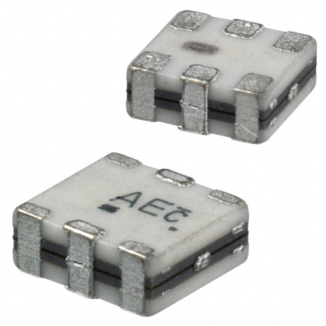
!Note(cid:129) Please read rating and !CAUTION (for storage, operating, rating, soldering, mounting and handling) in this catalog to prevent smoking and/or burning, etc. (cid:129) This catalog has only typical specifi cations. Therefore, please approve our product specifi cations or transact the approval sheet for product specifi cations before ordering. r r CERAFIL (CERAFIL 2.3-6.5MHz) for Audio/Visual Equipment 2.3-5.7MHz Chip Type SFSKB Series 5.2±0.1 (4) (1) The SFSKB series are SMD ceramic fi lters suitable for IR headphone applications. 3.8±0.1 ∗ (3.5) Center frequencies of 2.3, 2.8, 3.2, 3.8, 4.3, 4.8, 5.2, (2) (3) 5.7MHz are available. (4.93) Rcoemalpizaerde ds mwiathll, ctohninv eanntdio lnigahl tLwCe igfi lhtet rpsa.ckage, 1.35±0.15 Terminal Connection (0.1)1.5±0.1(2.0) 4-0.35 (1) : Input It helps to compose multi-channel circuit on one PCB. (2) : Output (3) (2) (3) : Ground Nccoo n Fftrreeibaqutuuteernse ctsyo athdeju rsetdmuecntito ins oref qpuroirdeudc otino nP CcoBs ta. nd it (1.6)1.0±0.1(0.1) 0.3±0.1(4) (1) 0.25±0.1 4-0.35 ( ∗Ts( 4 p o ))e: l e ::cE r RicaITfAiaeneeJpfcdre mae Mr:c e iu±onintn0onacl.rtlee1 hfsmolysr m Coetxohtd(eeienrrnw maislm e ) 1. SMD package in plastic emboss tape, available for automatic placing. 2. They are slim, at only 1.5mm max. thickness, and have a small mounting area (5.2x3.8mm) enabling fl exible PCB design. 3. Available for lead (Pb) free refl ow soldering process. 4. Operating temperature range: 0 to +70°C Storage temperature range: -55 to +85°C 5. No frequency adjustment is required in production process. 6. Small, thin and lightweight package compared with conventional LC fi lters c Applications 1. IR headphone 2. Set Top Box for satellite broadcasting 10 Nominal Center 3dB 20dB Insertion Spurious Spurious Input/Output Part Number Frequency (fn) Bandwidth Bandwidth Loss Attenuation(1) Attenuation(2) Impedance (MHz) (kHz) (kHz) (dB) (dB) (dB) (ohm) 25 min. 23 min. SFSKB2M30GF00-R1 2.300 fn±75 min. 650 max. 6.0 max. 1000 [within 1.3 to 1.8MHz] [within 2.8 to 3.3MHz] 25 min. 25 min. SFSKB2M80GF00-R1 2.800 fn±75 min. 650 max. 6.0 max. 1000 [within 1.8 to 2.3MHz] [within 3.3 to 3.8MHz] 30 min. 30 min. SFSKB3M20FF00-R1 3.200 fn±75 min. 650 max. 6.0 max. 1000 [within 2.2 to 2.8MHz] [within 3.8 to 4.2MHz] 30 min. 30 min. SFSKB3M80GF00-R1 3.800 fn±75 min. 650 max. 6.0 max. 1000 [within 2.8 to 3.2MHz] [within 4.3 to 4.8MHz] 30 min. 30 min. SFSKB4M30GF00-R1 4.300 fn±75 min. 650 max. 6.0 max. 1000 [within 3.3 to 3.8MHz] [within 4.8 to 5.3MHz] 30 min. 30 min. SFSKB4M80GF00-R1 4.800 fn±75 min. 650 max. 6.0 max. 1000 [within 3.8 to 4.3MHz] [within 5.2 to 5.8MHz] 30 min. 30 min. SFSKB5M20GF00-R1 5.200 fn±75 min. 650 max. 6.0 max. 1000 [within 4.2 to 4.8MHz] [within 5.7 to 6.2MHz] 30 min. 30 min. SFSKB5M70GF00-R1 5.700 fn±75 min. 650 max. 6.0 max. 1000 [within 4.7 to 5.2MHz] [within 6.2 to 6.7MHz] For safety purposes, connect the output of fi lters to the IF amplifi er through a D.C. blocking capacitor. Avoid applying a direct current to the output of ceramic fi lters. The order quantity should be an integral multiple of the "Minimum Quantity" shown in the package page. 34
!Note(cid:129) Please read rating and !CAUTION (for storage, operating, rating, soldering, mounting and handling) in this catalog to prevent smoking and/or burning, etc. (cid:129) This catalog has only typical specifi cations. Therefore, please approve our product specifi cations or transact the approval sheet for product specifi cations before ordering. c Standard Land Pattern Dimensions 1.8 2.0 1.8 1.3 1.6 1.3 (in mm) c Test Circuit SFSKB2M30GF00-R1/SFSKB3MZ0GF00-R1 SFSKB2M80GF00-R1/SFSKB3M20FF00-R1 R1 (1) (4) R1 (1) (4) Rg (2) (3) Rg (2) (3) E1 Cc R2 C2 E2 RVoFltmeter E1 Cc R2 C2 E2 RVoFltmeter S.S.G. S.S.G. R1+Rg=R2=1.0kΩ R1+Rg=R2=1.0kΩ Cc=22pF±5% (1) : Input Cc=39pF±5% (1) : Input C2=10pF (Including stray capacitance and (2) : Output C2=10pF (Including stray capacitance and (2) : Output Input capacitance of RF Voltmeter) (3) : Ground Input capacitance of RF Voltmeter) (3) : Ground E1 : S.S.G. Output Voltage (4) : Terminal for external capacitor E1 : S.S.G. Output Voltage (4) : Terminal for external capacitor SFSKB4M30GF00-R1/SFSKB5M70GF00-R1 SFSKB4M80GF00-R1 R1 (1) (4) R1 (1) (4) Rg (2) (3) Rg (2) (3) E1 Cc R2 C2 E2 RVoFltmeter E1 Cc R2 C2 E2 RVoFltmeter 10 S.S.G. S.S.G. R1+Rg=R2=1.0kΩ R1+Rg=R2=1.0kΩ Cc=33pF±5% (1) : Input Cc=15pF±5% (1) : Input C2=10pF (Including stray capacitance and (2) : Output C2=10pF (Including stray capacitance and (2) : Output Input capacitance of RF Voltmeter) (3) : Ground Input capacitance of RF Voltmeter) (3) : Ground E1 : S.S.G. Output Voltage (4) : Terminal for external capacitor E1 : S.S.G. Output Voltage (4) : Terminal for external capacitor SFSKB5M20GF00-R1 R1 (1) (4) Rg (2) (3) E1 Cc R2 C2 E2 RVoFltmeter S.S.G. R1+Rg=R2=1.0kΩ Cc=27pF±5% (1) : Input C2=10pF (Including stray capacitance and (2) : Output Input capacitance of RF Voltmeter) (3) : Ground E1 : S.S.G. Output Voltage (4) : Terminal for external capacitor 35
!Note(cid:129) Please read rating and !CAUTION (for storage, operating, rating, soldering, mounting and handling) in this catalog to prevent smoking and/or burning, etc. (cid:129) This catalog has only typical specifi cations. Therefore, please approve our product specifi cations or transact the approval sheet for product specifi cations before ordering. c Frequency Characteristics SFSKB2M30GF00-R1 SFSKB2M80GF00-R1 0 0 10 10 20 20 B) B) Attenuation (d345000 Attenuation (d345000 60 60 70 70 1.300 1.800 2.300 2.800 3.300 1.800 2.300 2.800 3.300 3.800 Frequency (MHz) Frequency (MHz) SFSKB3M20FF00-R1 SFSKB3M80GF00-R1 0 0 10 10 20 20 B) B) Attenuation (d345000 Attenuation (d345000 60 60 70 70 2.200 2.700 3.200 3.700 4.200 2.800 3.300 3.800 4.300 4.800 Frequency (MHz) Frequency (MHz) SFSKB4M30GF00-R1 SFSKB4M80GF00-R1 0 0 10 10 20 20 B) B) 10 Attenuation (d345000 Attenuation (d345000 60 60 70 70 3.300 3.800 4.300 4.800 5.300 3.800 4.300 4.800 5.300 5.800 Frequency (MHz) Frequency (MHz) SFSKB5M20GF00-R1 SFSKB5M70GF00-R1 0 0 10 10 20 20 B) B) Attenuation (d345000 Attenuation (d345000 60 60 70 70 4.200 4.700 5.200 5.700 6.200 4.700 5.200 5.700 6.200 6.700 Frequency (MHz) Frequency (MHz) 36
!Note(cid:129) Please read rating and !CAUTION (for storage, operating, rating, soldering, mounting and handling) in this catalog to prevent smoking and/or burning, etc. (cid:129) This catalog has only typical specifi cations. Therefore, please approve our product specifi cations or transact the approval sheet for product specifi cations before ordering. c Frequency Characteristics (Spurious) SFSKB2M30GF00-R1 SFSKB2M80GF00-R1 0 0 10 10 20 20 Attenuation (dB) 345000 Attenuation (dB) 345000 60 60 70 70 0.300 1.300 2.300 3.300 4.300 0.800 1.800 2.800 3.800 4.800 Frequency (MHz) Frequency (MHz) SFSKB3M20FF00-R1 SFSKB3M80GF00-R1 0 0 10 10 20 20 Attenuation (dB) 345000 Attenuation (dB) 345000 60 60 70 70 1.200 2.200 3.200 4.200 5.200 1.800 2.800 3.800 4.800 5.800 Frequency (MHz) Frequency (MHz) SFSKB4M30GF00-R1 SFSKB4M80GF00-R1 0 0 10 10 20 20 Attenuation (dB) 345000 Attenuation (dB) 345000 10 60 60 70 70 2.300 3.300 4.300 5.300 6.300 2.800 3.800 4.800 5.800 6.800 Frequency (MHz) Frequency (MHz) SFSKB5M20GF00-R1 SFSKB5M70GF00-R1 0 0 10 10 20 20 Attenuation (dB) 345000 Attenuation (dB) 345000 60 60 70 70 3.200 4.200 5.200 6.200 7.200 3.700 4.700 5.700 6.700 7.700 Frequency (MHz) Frequency (MHz) 37
!Note(cid:129) Please read rating and !CAUTION (for storage, operating, rating, soldering, mounting and handling) in this catalog to prevent smoking and/or burning, etc. (cid:129) This catalog has only typical specifi cations. Therefore, please approve our product specifi cations or transact the approval sheet for product specifi cations before ordering. r r CERAFIL (CERAFIL 455kHz) for Audio/Visual Equipment Chip Type SFPKA Series 7.0±0.3 3.0±0.3 SFPKA series for AM use is one of the most rdeisctoinmcmtiveen fdeaabtuler einst earsm heigdhia stee lfie lctetirvsi,t yh, ahviginhg such 7.5±0.3 MARKECINIOADGJE 8.4 max. stability and adjustment-free operation. 0.9±0.1 Additionally, its easy matching with IC helps create an max. easy circuit design. 5.0 1.5±0.3 2.0±0.3 c Features 2.0±0.3 1.5±0.3 1.6±0.3 Connection 1. The fi lters are mountable by automatic placers (1) (2) (3) ((12)):: IGnrpouutnd (3): Output and can be refl ow soldered and withstand (in mm) washing. 2. The fi lters are wide bandwidth and high selectivity, so they are suitable for car radio and multi-band radio. Center 6dB Selectivity (-) Selectivity (+) Insertion Input/Output Part Number Frequency (fo) Bandwidth Loss Impedance Element (kHz) (kHz) (dB) (dB) (dB) (ohm) SFPKA450KH1A-R1 450.0 ±1.0kHz fn±3.0 min. 40 min.[fn-9kHz] 40 min.[fn+9kHz] 6.0 max. 2000 4 SFPKA450KG1A-R1 450.0 ±1.0kHz fn±4.5 min. 40 min.[fn-10kHz] 40 min.[fn+10kHz] 6.0 max. 1500 4 Area of Insertion Loss: at minimum loss point Center frequency (fo) is defi ned by the center of 6dB bandwidth. (fn) means nominal center frequency (450kHz). For safety purposes, connect the output of fi lters to the IF amplifi er through a D.C. blocking capacitor. Avoid applying a direct current to the output of ceramic fi lters. The order quantity should be an integral multiple of the "Minimum Quantity" shown in the package page. c Standard Land Pattern Dimensions c Recommended IFT Type Item SFPKA 6.95 2.475 2.0 0.8 Winding Specification (1)—(2) (2)—(3) (4)—(6) 1.6 S((32)) (4)S (1) (6) 60T 125T 28T 11 7.45 (Bottom view) 1.55 No load Qu 40 0.925 1.21.0 2.0 0.9 (cid:0)(cid:0)(cid:115)(cid:0)(cid:45)T(cid:65)u(cid:84)n(cid:67)i(cid:72)n(cid:73)g(cid:78) (cid:71)C(cid:0)(cid:79)a(cid:70)p(cid:0)(cid:35)ac(cid:37)it(cid:50)a(cid:33)nc(cid:38)e(cid:41)(cid:44)r(cid:0)(cid:51)(cid:38)(cid:48)(cid:43)(cid:33)(cid:0)(cid:83)(cid:69)(cid:82)(cid:73)(cid:69)(cid:83)(cid:0)(cid:87)(cid:73)(cid:84)(cid:72)(cid:0)(cid:41)(cid:38)(cid:52)1(cid:0)(cid:73)8(cid:83)0(cid:0)(cid:68)p(cid:69)F(cid:67)(cid:73)(cid:68)(cid:69)(cid:68)(cid:0)(cid:66)(cid:89)(cid:0)(cid:84)(cid:72)(cid:69)(cid:0)(cid:49)(cid:85)(cid:0)(cid:79)(cid:70)(cid:0)(cid:41)(cid:38)(cid:52)(cid:0) (cid:65)(cid:78)(cid:68)(cid:0)(cid:41)(cid:38)(cid:52)(cid:0)(cid:83)(cid:69)(cid:67)(cid:79)(cid:78)(cid:68)(cid:65)(cid:82)(cid:89)(cid:0)(cid:83)(cid:73)(cid:68)(cid:69)(cid:0)(cid:73)(cid:77)(cid:80)(cid:69)(cid:68)(cid:65)(cid:78)(cid:67)(cid:69)(cid:12)(cid:0)(cid:92)(cid:58)(cid:18)(cid:92)(cid:14)(cid:0)(cid:51)(cid:69)(cid:84)(cid:0)(cid:84)(cid:72)(cid:69)(cid:0)(cid:49)(cid:85)(cid:0)(cid:65)(cid:84)(cid:0)(cid:65)(cid:66)(cid:79)(cid:85)(cid:84)(cid:0)(cid:20)(cid:16)(cid:0)(cid:66)(cid:69)(cid:67)(cid:65)(cid:85)(cid:83)(cid:69)(cid:0) (in mm) (cid:65)(cid:0)(cid:49)(cid:85)(cid:0)(cid:86)(cid:65)(cid:76)(cid:85)(cid:69)(cid:0)(cid:87)(cid:72)(cid:73)(cid:67)(cid:72)(cid:0)(cid:73)(cid:83)(cid:0)(cid:84)(cid:79)(cid:79)(cid:0)(cid:72)(cid:73)(cid:71)(cid:72)(cid:0)(cid:8)(cid:69)(cid:14)(cid:71)(cid:14)(cid:12)(cid:25)(cid:16)(cid:9)(cid:0)(cid:77)(cid:65)(cid:89)(cid:0)(cid:80)(cid:82)(cid:79)(cid:68)(cid:85)(cid:67)(cid:69)(cid:0)(cid:82)(cid:73)(cid:80)(cid:80)(cid:76)(cid:69)(cid:0)(cid:73)(cid:78)(cid:0)(cid:84)(cid:72)(cid:69)(cid:0)(cid:87)(cid:65)(cid:86)(cid:69)(cid:70)(cid:79)(cid:82)(cid:77)(cid:14)(cid:0) (cid:41)(cid:84)(cid:0)(cid:73)(cid:83)(cid:0)(cid:82)(cid:69)(cid:67)(cid:79)(cid:77)(cid:77)(cid:69)(cid:78)(cid:68)(cid:69)(cid:68)(cid:0)(cid:84)(cid:79)(cid:0)(cid:77)(cid:65)(cid:84)(cid:67)(cid:72)(cid:0)(cid:84)(cid:72)(cid:69)(cid:0)(cid:73)(cid:77)(cid:80)(cid:69)(cid:68)(cid:65)(cid:78)(cid:67)(cid:69)(cid:0)(cid:79)(cid:70)(cid:0)(cid:92)(cid:58)(cid:18)(cid:92)(cid:0)(cid:87)(cid:73)(cid:84)(cid:72)(cid:0)(cid:84)(cid:72)(cid:65)(cid:84)(cid:0)(cid:79)(cid:70)(cid:0)(cid:84)(cid:72)(cid:69)(cid:0) (cid:35)(cid:37)(cid:50)(cid:33)(cid:38)(cid:41)(cid:44)r(cid:14) c Test Circuit R1 (1) (3) (2) RF Voltmeter Rg E1 R2 E2 S.S.G. 0dBm (1): Input Rg+R1=R2=Input/Output Impedance (2): Ground E1: S.S.G. Output Voltage (3): Output 38
!Note(cid:129) Please read rating and !CAUTION (for storage, operating, rating, soldering, mounting and handling) in this catalog to prevent smoking and/or burning, etc. (cid:129) This catalog has only typical specifi cations. Therefore, please approve our product specifi cations or transact the approval sheet for product specifi cations before ordering. c Frequency Characteristics SFPKA450KH1A-R1 SFPKA450KG1A-R1 0 400 0 400 10 360 10 360 20 320 20 320 30 280 30 280 Attenuation (dB) 465000 221046000 G.D.T. (μsec.) Attenuation (dB) 465000 221046000 G.D.T. (μsec.) 70 120 70 120 80 80 80 80 90 40 90 40 100 0 100 0 425 450 475 425 450 475 Frequency (kHz) Frequency (kHz) 11 39
!Note(cid:129) Please read rating and !CAUTION (for storage, operating, rating, soldering, mounting and handling) in this catalog to prevent smoking and/or burning, etc. (cid:129) This catalog has only typical specifi cations. Therefore, please approve our product specifi cations or transact the approval sheet for product specifi cations before ordering. r r CERAFIL (CERAFIL 455kHz) for Audio/Visual Equipment Lead Type SFPLA/CFWLA Series 8.0±0.3 SsuFiPtaLbAle/C inFtWermLAe dsieartiee sfi lftoerr sA, Mha uvsineg i ss uocnhe of the most MARKEIINAJG 7.0±0.3 CODE distinctive features as high selectivity, high sotpaebrialittyio, nh.i gAhd daitttieonnuaallyti,o ints, aenads ya mdjuastctmhinegn tw-fritehe I C 7.3±0.3 0.8±0.1 0.3±0.1 hTehlips sis c trheea tme oasnt esausitya bclierc fuoitr dcaers isgtne.reo and 0.15±0.05 21.5 max..7±0.3 13.0±0.3.2±0.5 0.6±0.1 all band radio with high attenuation. SFPLA Series (3)(2) (1) 4.2±0.3 C(((123o))) n::: n IGOencrupottuipoutunntd (in mm) 3.3±0.5 11.0±0.5 MARKECINIOADGJE 7.0±0.5 7.5±0.5 0.8±0.1 1.5 max. 0.15 3.5±0.5 2.9±0.3 22..99±—00.3.3 2.6±0.3 0.6±0.1 1.2±0.5 Connection CFWLA Series 1.35±0.5 ((45))(3) (2) (1) 4.3±0.3 ( 2 ) ( 3 ) (((415)))::: GIOnrupotuuptnudt 2.3±0.5 2.0±0.3 (in mm) Center 6dB Selectivity (-) Selectivity (+) Insertion Input/Output Part Number Frequency (fo) Bandwidth Loss Impedance Element (kHz) (kHz) (dB) (dB) (dB) (ohm) SFPLA450KJ1A-B0 450.0 ±1.0kHz fn±2.0 min. 40 min.[fn-7.5kHz] 40 min.[fn+7.5kHz] 6.0 max. 2000 4 SFPLA450KH1A-B0 450.0 ±1.0kHz fn±3.0 min. 40 min.[fn-9kHz] 40 min.[fn+9kHz] 6.0 max. 2000 4 CFWLA450KJFA-B0 450.0 (fn) fn±2.0 min. 50 min.[fn-7.5kHz] 50 min.[fn+7.5kHz] 7.0 max. 2000 6 CFWLA450KHFA-B0 450.0 (fn) fn±3.0 min. 50 min.[fn-9kHz] 50 min.[fn+9kHz] 6.0 max. 2000 6 Area of Insertion Loss: at minimum loss point Center frequency (fo) is defi ned by the center of 6dB bandwidth. (fn) means nominal center frequency (450kHz). For safety purposes, connect the output of fi lters to the IF amplifi er through a D.C. blocking capacitor. Avoid applying a direct current to the output of ceramic fi lters. The order quantity should be an integral multiple of the "Minimum Quantity" shown in the package page. 12 c Recommended IFT c Test Circuit Type SFPLA/CFWLA Item 7x7mm IFT Winding Specification (1)—(2) (2)—(3) (4)—(6) R1 Input Output S(3) (4)S Rg (2) (1) (6) 60T 125T 28T RF (Bottom view) SSG R2 Voltmeter No load Qu 40 Ground Tuning Capacitance 180pF (cid:0)(cid:0)(cid:115)(cid:0)(cid:45)(cid:65)(cid:84)(cid:67)(cid:72)(cid:73)(cid:78)(cid:71)(cid:0)(cid:79)(cid:70)(cid:0)(cid:35)(cid:37)(cid:50)(cid:33)(cid:38)(cid:41)(cid:44)r(cid:0)(cid:51)(cid:38)(cid:48)(cid:44)(cid:33)(cid:15)(cid:35)(cid:38)(cid:55)(cid:44)(cid:33)(cid:0)(cid:83)(cid:69)(cid:82)(cid:73)(cid:69)(cid:83)(cid:0)(cid:87)(cid:73)(cid:84)(cid:72)(cid:0)(cid:41)(cid:38)(cid:52)(cid:0)(cid:73)(cid:83)(cid:0)(cid:68)(cid:69)(cid:67)(cid:73)(cid:68)(cid:69)(cid:68)(cid:0)(cid:66)(cid:89)(cid:0)(cid:84)(cid:72)(cid:69)(cid:0) Rg+R1 =R2 : Input/Output Impedance (cid:49)(cid:85)(cid:0)(cid:79)(cid:70)(cid:0)(cid:41)(cid:38)(cid:52)(cid:0)(cid:65)(cid:78)(cid:68)(cid:0)(cid:41)(cid:38)(cid:52)(cid:0)(cid:83)(cid:69)(cid:67)(cid:79)(cid:78)(cid:68)(cid:65)(cid:82)(cid:89)(cid:0)(cid:83)(cid:73)(cid:68)(cid:69)(cid:0)(cid:73)(cid:77)(cid:80)(cid:69)(cid:68)(cid:65)(cid:78)(cid:67)(cid:69)(cid:12)(cid:0)(cid:92)(cid:58)(cid:18)(cid:92)(cid:14)(cid:0)(cid:51)(cid:69)(cid:84)(cid:0)(cid:84)(cid:72)(cid:69)(cid:0)(cid:49)(cid:85)(cid:0)(cid:65)(cid:84)(cid:0)(cid:65)(cid:66)(cid:79)(cid:85)(cid:84)(cid:0)(cid:20)(cid:16)(cid:0) (cid:66)(cid:69)(cid:67)(cid:65)(cid:85)(cid:83)(cid:69)(cid:0)(cid:65)(cid:0)(cid:49)(cid:85)(cid:0)(cid:86)(cid:65)(cid:76)(cid:85)(cid:69)(cid:0)(cid:87)(cid:72)(cid:73)(cid:67)(cid:72)(cid:0)(cid:73)(cid:83)(cid:0)(cid:84)(cid:79)(cid:79)(cid:0)(cid:72)(cid:73)(cid:71)(cid:72)(cid:0)(cid:8)(cid:69)(cid:14)(cid:71)(cid:14)(cid:12)(cid:25)(cid:16)(cid:9)(cid:0)(cid:77)(cid:65)(cid:89)(cid:0)(cid:80)(cid:82)(cid:79)(cid:68)(cid:85)(cid:67)(cid:69)(cid:0)(cid:82)(cid:73)(cid:80)(cid:80)(cid:76)(cid:69)(cid:0)(cid:73)(cid:78)(cid:0)(cid:84)(cid:72)(cid:69)(cid:0) (cid:87)(cid:65)(cid:86)(cid:69)(cid:70)(cid:79)(cid:82)(cid:77)(cid:14)(cid:0)(cid:41)(cid:84)(cid:0)(cid:73)(cid:83)(cid:0)(cid:82)(cid:69)(cid:67)(cid:79)(cid:77)(cid:77)(cid:69)(cid:78)(cid:68)(cid:69)(cid:68)(cid:0)(cid:84)(cid:79)(cid:0)(cid:77)(cid:65)(cid:84)(cid:67)(cid:72)(cid:0)(cid:84)(cid:72)(cid:69)(cid:0)(cid:73)(cid:77)(cid:80)(cid:69)(cid:68)(cid:65)(cid:78)(cid:67)(cid:69)(cid:0)(cid:79)(cid:70)(cid:0)(cid:92)(cid:58)(cid:18)(cid:92)(cid:0)(cid:87)(cid:73)(cid:84)(cid:72)(cid:0)(cid:84)(cid:72)(cid:65)(cid:84)(cid:0)(cid:79)(cid:70)(cid:0) (cid:84)(cid:72)(cid:69)(cid:0)(cid:35)(cid:37)(cid:50)(cid:33)(cid:38)(cid:41)(cid:44)r(cid:14) 40
!Note(cid:129) Please read rating and !CAUTION (for storage, operating, rating, soldering, mounting and handling) in this catalog to prevent smoking and/or burning, etc. (cid:129) This catalog has only typical specifi cations. Therefore, please approve our product specifi cations or transact the approval sheet for product specifi cations before ordering. c Frequency Characteristics IFT+SFPLA450KH1A-B0 IFT+CFWLA450KHFA-B0 0 0 10 10 20 20 Attenuation (dB) 3400 Attenuation (dB) 4300 50 50 60 60 70 430 440 450 460 470 70 430 440 450 460 470 Frequency (kHz) Frequency (kHz) c Frequency Characteristics (Spurious) IFT+SFPLA450KH1A-B0 IFT+CFWLA450KHFA-B0 0 0 10 10 20 20 Attenuation (dB)543000 Attenuation (dB)543000 60 60 70 70 80 80 0 1 2 3 4 5 6 7 8 9 10 0 1 2 3 4 5 6 7 8 9 10 Frequency (MHz) Frequency (MHz) 12 41
!Note(cid:129) Please read rating and !CAUTION (for storage, operating, rating, soldering, mounting and handling) in this catalog to prevent smoking and/or burning, etc. (cid:129) This catalog has only typical specifi cations. Therefore, please approve our product specifi cations or transact the approval sheet for product specifi cations before ordering. r r CERAFIL (CERAFIL 455kHz) for Audio/Visual Equipment For AM Stereo Wide Bandwidth Type SFPLA/CFWLA/CFULA Series 8.0±0.3 SthFeP mLAos/Ct sFuUitLaAb/lCe FinWteLrmA esdeiraietes fif oltre ArsM, h uasvein igs sounceh o f MARKEIINAJG 7.0±0.3 CODE distinctive features as high selectivity, high stability, hAidgdhi taiottneanlluya, tiitosn e, aasnyd m aadtjuchstinmge wnti-tfhr eICe ohpeelpras tciorne.a te 7.3±0.3 0.8±0.1 0.3±0.1 aEns peeacsiay llcyi,r cCuFitU dLeAsi/gCnF.WLA_Y series improves the 0.15±0.05 21.5 max..7±0.3 13.0±0.3.2±0.5 0.6±0.1 frequency fi delity in the high sound area of an AM stereo with its wide band and fl at characteristics of SFPLA Series (3)(2) (1) 4.2±0.3 C(((123o))) n::: n IGOencrupottuipoutunntd group delay time. (in mm) 3.3±0.5 11.0±0.5 8.0±0.3 MARKECINIOADGJE 7.0±0.5 MARKECINIOADGJE 7.0±0.3 7.5±0.5 0.8±0.1 1.5 max. 7.3±0.3 0.8±0.1 0.3±0.1 2.90±.01.53 22..99±—00.3.3 2.6±3.5±0.50.3 0.6±0.1 02..175±±00.3.05 1.5 max. 1.2±03.0±0.3.5 0.6±0.1 CFWLA Series 1.35±0.5 ((45))(3) (2) (1) 1.2±4.3±0.30.5 C ( 2 o ) (n 3 n ) e(((415c)))t:::i o GIOnnrupotuuptnudt CFULA Series (3)(2) (1) 4.2±0.3 C(((123o))):::n IGOnnerupoctuputitounntd 2.3±0.5 2.0±0.3 (in mm) 3.3±0.5 (in mm) Center 6dB Selectivity (-) Selectivity (+) Insertion GDT 20µsec. Input/Output Part Number Frequency (fo) Bandwidth Loss Bandwidth Impedance Element (kHz) (kHz) (dB) (dB) (dB) (kHz) (ohm) SFPLA450KG1A-B0 450.0 ±1.0kHz fn±4.5 min. 30 min.[fn-9kHz] 30 min.[fn+9kHz] 6.0 max. - 2000 4 SFPLA450KF1A-B0 450.0 ±1.0kHz fn±6.0 min. 40 min.[fn-12.5kHz] 40 min.[fn+12.5kHz] 6.0 max. - 2000 4 SFPLA450KE1A-B0 450.0 ±1.0kHz fn±7.5 min. 40 min.[fn-15kHz] 40 min.[fn+15kHz] 6.0 max. - 1500 4 SFPLA450KD1A-B0 450.0 ±1.0kHz fn±10.0 min. 40 min.[fn-20kHz] 40 min.[fn+20kHz] 4.0 max. - 1500 4 CFULA450KG1Y-B0 450.0 ±1.0kHz fn±4.5 min. 40 min.[fn-15kHz] 40 min.[fn+15kHz] 10.0 max. fn±3 2000 4 CFULA450KF1Y-B0 450.0 ±1.0kHz fn±6.0 min. 40 min.[fn-17.5kHz] 40 min.[fn+17.5kHz] 9.0 max. fn±4 2000 4 CFULA450KD1Y-B0 450.0 ±1.0kHz fn±10.0 min. 40 min.[fn-25kHz] 40 min.[fn+25kHz] 7.0 max. fn±7 1500 4 CFWLA450KG1Y-B0 450.0 ±1.0kHz fn±4.5 min. 50 min.[fn-15kHz] 50 min.[fn+15kHz] 11.0 max. fn±4 2000 6 CFWLA450KF1Y-B0 450.0 ±1.0kHz fn±6.0 min. 50 min.[fn-17.5kHz] 50 min.[fn+17.5kHz] 10.0 max. fn±5 2000 6 CFWLA450KD1Y-B0 450.0 ±1.0kHz fn±10.0 min. 50 min.[fn-25kHz] 50 min.[fn+25kHz] 8.0 max. fn±8 1500 6 CFWLA450KGFA-B0 450.0 (fn) fn±4.5 min. 50 min.[fn-10kHz] 50 min.[fn+10kHz] 6.0 max. - 2000 6 CFWLA450KFFA-B0 450.0 (fn) fn±6.0 min. 50 min.[fn-12.5kHz] 50 min.[fn+12.5kHz] 6.0 max. - 2000 6 13 CFWLA450KEFA-B0 450.0 (fn) fn±7.5 min. 50 min.[fn-15kHz] 50 min.[fn+15kHz] 6.0 max. - 1500 6 CFWLA450KDFA-B0 450.0 (fn) fn±10.0 min. 50 min.[fn-20kHz] 50 min.[fn+20kHz] 4.0 max. - 1500 6 Area of Insertion Loss: at minimum loss point Center frequency (fo) is defi ned by the center of 6dB bandwidth. (fn) means nominal center frequency (450kHz). For safety purposes, connect the output of fi lters to the IF amplifi er through a D.C. blocking capacitor. Avoid applying a direct current to the output of ceramic fi lters. The order quantity should be an integral multiple of the "Minimum Quantity" shown in the package page. 42
!Note(cid:129) Please read rating and !CAUTION (for storage, operating, rating, soldering, mounting and handling) in this catalog to prevent smoking and/or burning, etc. (cid:129) This catalog has only typical specifi cations. Therefore, please approve our product specifi cations or transact the approval sheet for product specifi cations before ordering. c Recommended IFT c Test Circuit Type SFPLA/CFULA/CFWLA Item 7x7mm IFT Winding Specification (1)—(2) (2)—(3) (4)—(6) R1 Input Output S(3) (4)S Rg (2) (1) (6) 60T 125T 28T RF (Bottom view) SSG R2 Voltmeter No load Qu 40 Ground Tuning Capacitance 180pF (cid:0)(cid:0)(cid:115)(cid:0)(cid:45)(cid:65)(cid:84)(cid:67)(cid:72)(cid:73)(cid:78)(cid:71)(cid:0)(cid:79)(cid:70)(cid:0)(cid:35)(cid:37)(cid:50)(cid:33)(cid:38)(cid:41)(cid:44)r(cid:0)(cid:51)(cid:38)(cid:48)(cid:44)(cid:33)(cid:15)(cid:35)(cid:38)(cid:53)(cid:44)(cid:33)(cid:15)(cid:35)(cid:38)(cid:55)(cid:44)(cid:33)(cid:0)(cid:83)(cid:69)(cid:82)(cid:73)(cid:69)(cid:83)(cid:0)(cid:87)(cid:73)(cid:84)(cid:72)(cid:0)(cid:41)(cid:38)(cid:52)(cid:0)(cid:73)(cid:83)(cid:0)(cid:68)(cid:69)(cid:67)(cid:73)(cid:68)(cid:69)(cid:68)(cid:0) Rg+R1 =R2 : Input/Output Impedance (cid:66)(cid:89)(cid:0)(cid:84)(cid:72)(cid:69)(cid:0)(cid:49)(cid:85)(cid:0)(cid:79)(cid:70)(cid:0)(cid:41)(cid:38)(cid:52)(cid:0)(cid:65)(cid:78)(cid:68)(cid:0)(cid:41)(cid:38)(cid:52)(cid:0)(cid:83)(cid:69)(cid:67)(cid:79)(cid:78)(cid:68)(cid:65)(cid:82)(cid:89)(cid:0)(cid:83)(cid:73)(cid:68)(cid:69)(cid:0)(cid:73)(cid:77)(cid:80)(cid:69)(cid:68)(cid:65)(cid:78)(cid:67)(cid:69)(cid:12)(cid:0)(cid:92)(cid:58)(cid:18)(cid:92)(cid:14)(cid:0)(cid:51)(cid:69)(cid:84)(cid:0)(cid:84)(cid:72)(cid:69)(cid:0)(cid:49)(cid:85)(cid:0)(cid:65)(cid:84)(cid:0) (cid:65)(cid:66)(cid:79)(cid:85)(cid:84)(cid:0)(cid:20)(cid:16)(cid:0)(cid:66)(cid:69)(cid:67)(cid:65)(cid:85)(cid:83)(cid:69)(cid:0)(cid:65)(cid:0)(cid:49)(cid:85)(cid:0)(cid:86)(cid:65)(cid:76)(cid:85)(cid:69)(cid:0)(cid:87)(cid:72)(cid:73)(cid:67)(cid:72)(cid:0)(cid:73)(cid:83)(cid:0)(cid:84)(cid:79)(cid:79)(cid:0)(cid:72)(cid:73)(cid:71)(cid:72)(cid:0)(cid:8)(cid:69)(cid:14)(cid:71)(cid:14)(cid:12)(cid:25)(cid:16)(cid:9)(cid:0)(cid:77)(cid:65)(cid:89)(cid:0)(cid:80)(cid:82)(cid:79)(cid:68)(cid:85)(cid:67)(cid:69)(cid:0) (cid:82)(cid:73)(cid:80)(cid:80)(cid:76)(cid:69)(cid:0)(cid:73)(cid:78)(cid:0)(cid:84)(cid:72)(cid:69)(cid:0)(cid:87)(cid:65)(cid:86)(cid:69)(cid:70)(cid:79)(cid:82)(cid:77)(cid:14)(cid:0)(cid:41)(cid:84)(cid:0)(cid:73)(cid:83)(cid:0)(cid:82)(cid:69)(cid:67)(cid:79)(cid:77)(cid:77)(cid:69)(cid:78)(cid:68)(cid:69)(cid:68)(cid:0)(cid:84)(cid:79)(cid:0)(cid:77)(cid:65)(cid:84)(cid:67)(cid:72)(cid:0)(cid:84)(cid:72)(cid:69)(cid:0)(cid:73)(cid:77)(cid:80)(cid:69)(cid:68)(cid:65)(cid:78)(cid:67)(cid:69)(cid:0)(cid:79)(cid:70)(cid:0)(cid:92)(cid:58)(cid:18)(cid:92)(cid:0) (cid:87)(cid:73)(cid:84)(cid:72)(cid:0)(cid:84)(cid:72)(cid:65)(cid:84)(cid:0)(cid:79)(cid:70)(cid:0)(cid:84)(cid:72)(cid:69)(cid:0)(cid:35)(cid:37)(cid:50)(cid:33)(cid:38)(cid:41)(cid:44)r(cid:14) c Frequency Characteristics IFT+SFPLA450KF1A-B0 IFT+CFWLA450KFFA-B0 0 0 10 10 20 20 Attenuation (dB) 3400 Attenuation (dB) 4300 50 50 60 60 70 430 440 450 460 470 70430 440 450 460 470 Frequency (kHz) Frequency (kHz) IFT+CFULA450KF1Y-B0 IFT+CFWLA450KF1Y-B0 0 0 10 10 20 200 20 200 Attenuation (dB) 4300 1000 Delay Time (μsec.) Attenuation (dB) 4300 1000 Delay Time (μsec.) 50 Group 50 Group 60 60 70430 440 450 460 470 70430 440 450 460 470 Frequency (kHz) Frequency (kHz) 13 43
!Note(cid:129) Please read rating and !CAUTION (for storage, operating, rating, soldering, mounting and handling) in this catalog to prevent smoking and/or burning, etc. (cid:129) This catalog has only typical specifi cations. Therefore, please approve our product specifi cations or transact the approval sheet for product specifi cations before ordering. CERAFILr 455kHz SFp Series Temperature Characteristics c SFPLA450KH1A-B0 Center Frequency(kHz)+-011 -20 0 20 40 Tem60perature (°C)80 +1 Insertion Loss(dB) -01 -20 0 20 40 Tem60perature (°C)80 +1 Temperature (°C) 3dB Bandwidth(kHz) -01 -20 0 20 40 60 80 44
!Note(cid:129) Please read rating and !CAUTION (for storage, operating, rating, soldering, mounting and handling) in this catalog to prevent smoking and/or burning, etc. (cid:129) This catalog has only typical specifi cations. Therefore, please approve our product specifi cations or transact the approval sheet for product specifi cations before ordering. r CERAFIL (Ceramic Trap) for Audio/Visual Equipment 4.5-6.5MHz Chip Type TPSKA Series SMD ceramic trap TPSKA_B is a small and thin SMD trap sealed with a metal cap recommended for LCD-TVs, and small and thin tuners. 7.9±0.2 3.0±0.1 1.8±0.2 c Features 0.5±0.1 8.5±0.2 3.8±0.2 1. High attenuation and high performance group 0.6±0.2 1.0±0.1 delay time 1.3±0.2 2. Small and thin package 0.3±0.1 3. Refl ow-solderable 1.3±0.2 (1) : Input (2) : Ground (1) (2) (3) (3) : Output (in mm) 2.5±0.2 2.5±0.2 Nominal Center Frequency (fn1) Attenuation (at fn1) 30dB Attenuation BW (fn1) Part Number (MHz) (dB) (kHz) TPSKA4M50B00-R3 4.500 35 min. 50 min. TPSKA5M50B00-R3 5.500 35 min. 70 min. TPSKA6M00B00-R3 6.000 35 min. 70 min. TPSKA6M50B00-R3 6.500 35 min. 70 min. For safety purposes, connect the output of fi lters to the IF amplifi er through a D.C. blocking capacitor. Avoid applying a direct current to the output of ceramic fi lters. The order quantity should be an integral multiple of the "Minimum Quantity" shown in the package page. c Standard Land Pattern Dimensions c Test Circuit L 1.0 1.0 1.0 R1 1.5 1.5 Rg 50Ω R2 4.8 S.S.G. RVoFltmeter Rg=50Ω L=15μH R1=330Ω R2=1.0kΩ (in mm) c Frequency Characteristics TPSKA4M50B00-R3 TPSKA5M50B00-R3 0 0 10 10 Attenuation (dB) 234000 Attenuation (dB) 234000 14 50 50 60 60 70 70 4.0 4.1 4.2 4.3 4.4 4.5 4.6 4.7 4.8 4.9 5.0 5.0 5.1 5.2 5.3 5.4 5.5 5.6 5.7 5.8 5.9 6.0 Frequency (MHz) Frequency (MHz) Continued on the following page. 45
!Note(cid:129) Please read rating and !CAUTION (for storage, operating, rating, soldering, mounting and handling) in this catalog to prevent smoking and/or burning, etc. (cid:129) This catalog has only typical specifi cations. Therefore, please approve our product specifi cations or transact the approval sheet for product specifi cations before ordering. Continued from the preceding page. c Frequency Characteristics TPSKA6M00B00-R3 TPSKA6M50B00-R3 0 0 10 10 Attenuation (dB) 234000 Attenuation (dB) 234000 50 50 60 60 70 70 5.5 5.6 5.7 5.8 5.9 6.0 6.1 6.2 6.3 6.4 6.5 6.0 6.1 6.2 6.3 6.4 6.5 6.6 6.7 6.8 6.9 7.0 Frequency (MHz) Frequency (MHz) c Frequency Characteristics (Spurious) TPSKA4M50B00-R3 TPSKA5M50B00-R3 0 700 0 1000 10 600 10 800 20 500 20 600 Attenuation (dB) 345000 432000000 G.D.T. (nsec) Attenuation (dB) 345000 4200000 G.D.T. (nsec.) 60 100 60 70 0 70 80 80 0 1.0 2.0 3.0 4.0 5.0 0 1.0 2.0 3.0 4.0 5.0 6.0 7.0 8.0 9.0 10.0 Frequency (MHz) Frequency (MHz) TPSKA6M00B00-R3 TPSKA6M50B00-R3 0 1000 0 1000 10 800 10 800 20 600 20 600 Attenuation (dB) 345000 4200000 G.D.T. (nsec.) Attenuation (dB) 345000 4200000 G.D.T. (nsec.) 60 60 70 70 80 80 0 1.0 2.0 3.0 4.0 5.0 6.0 7.0 8.0 9.0 10.0 0 1.0 2.0 3.0 4.0 5.0 6.0 7.0 8.0 9.0 10.0 Frequency (MHz) Frequency (MHz) 14 46
!Note(cid:129) Please read rating and !CAUTION (for storage, operating, rating, soldering, mounting and handling) in this catalog to prevent smoking and/or burning, etc. (cid:129) This catalog has only typical specifi cations. Therefore, please approve our product specifi cations or transact the approval sheet for product specifi cations before ordering. r CERAFIL (Ceramic Discriminator) for Audio/Visual Equipment 10.7MHz Ultra Thin Chip Type CDSCB Series CDSCB10M7 series forms a resonator on a piezoelectric 0.3±0.2 4.5±0.1 coebrtaaminsic sstuabbsletr daetem. oInd ucolamtiobnin cahtiaorna wctiethri sICticss, tihni sa twypidee 2.0±0.1 1.4 max. bandwidth. 0.2±0.2 0.4±0.05 4.1 max. They have 1.0mm max. thickness and small mounting area max. (4.5x2.0mm). 1.0 0.4(ref.) 0.4(ref.) 0.8±0.1 0.8±0.1 c Features 1. Compact and high reliability and recommended for automotive applications. 1.5±0.1 1.5±0.1 (in mm) 2. Can be combined with various ICs. The IC is determined by the last number in the part number. 3. Stable demodulation characteristics can be obtained without adjustment. 4. Stable temperature characteristics. 5. Available lead (Pb) free solder refl ow. Center Recovered Recovered Distortion S Curve Part Number Frequency (fo) Audio 3dB BW Audio Output IC (MHz) (kHz) (mV) (%) (mV) CDSCB10M7GA105A-R0 10.700 ±30kHz 220 min. 110 min. 1.5 max. - TEA5757HL CDSCB10M7GA113-R0 10.700 ±30kHz 300 min. 110 min. 1.0 max. - TA2154FN CDSCB10M7GA119-R0 10.700 ±30kHz 500 min. 75 min. 1.0 max. - TRF6901 CDSCB10M7GA121-R0 10.700 ±30kHz 390 min. 80 min. 1.0 max. - LV23100V CDSCB10M7GA135-R0 10.700 ±30kHz 155 min. 75 min. - - TH71101 CDSCB10M7GA136-R0 10.700 ±30kHz 140 min. 120 min. - - TH7122 CDSCB10M7GF072-R0 10.700 (fn) fn±150 min. 130 min. 2.0 max. - TA31161 CDSCB10M7GF107S-R0 10.700 (fn) fn±80 min. 52 min. 3.0 max. - TA31272FN CDSCB10M7GF109-R0 10.700 (fn) fn±100 min. 170 min. 3.0 max. - TK14588V CDSCB10M7GF123-R0 10.700 (fn) - - - 900 min. TA31275FN CDSCB10M7GF123S-R0 10.700 (fn) - - - 900 min. TA31275FN CDSCB10M7GF126-R0 10.700 (fn) - - - 400 min. NJM2295AV (fn) means nominal center frequency (10.700MHz). For safety purposes, avoid applying a direct current between the terminals. The order quantity should be an integral multiple of the "Minimum Quantity" shown in the package page. c Standard Center Frequency Rank Code CODE 30kHz Step 25kHz Step D 10.64MHz±30kHz 10.650MHz±25kHz B 10.67MHz±30kHz 10.675MHz±25kHz A 10.70MHz±30kHz 10.700MHz±25kHz C 10.73MHz±30kHz 10.725MHz±25kHz E 10.76MHz±30kHz 10.750MHz±25kHz Z Combination A, B, C, D, E M Combination A, B, C 15 47
!Note(cid:129) Please read rating and !CAUTION (for storage, operating, rating, soldering, mounting and handling) in this catalog to prevent smoking and/or burning, etc. (cid:129) This catalog has only typical specifi cations. Therefore, please approve our product specifi cations or transact the approval sheet for product specifi cations before ordering. c Standard Land Pattern Dimensions 3.0 2.6 1.0 2.0 1.0 (in mm) c Test Circuit CDSCB10M7GA105A-R0 CDSCB10M7GA113-R0 Vcc (1.2V) Vcc (3.0V) 0.1μ + 101μ+48 47 46 45 44 43 42 41 40 39 38 3736 0.1μ 0.01μ 0.01μ 0.01μ 100μ 30 29 28 27 26 25 24 23 22 21 20 19 18 17 16 2 35 S.S.G. 3 34 TA2154FN (TOSHIBA) 4 33 1 2 3 4 5 6 7 8 9 10 11 12 13 14 15 + 5 32 76 T(EPAH5IL7I5P7SH)L 3301 X 680p 2.2μ 8 29 0.01μ 0.01μ D.C. OUT AF OUT 9 28 100k 10 27 S.S.G. X: CDSCB10M7GUAn1i1t 3C-:R F0 11 26 R: Ω 10 DC OUT 12 25 13 14 15 16 17 18 19 20 21 22 23 24 330p 4.7μ + X 0.47μ 0.1μ 0.1μ 0.22μ 150 C (n) C (p) X: CDSCB10M7GAU1n0i5t AC-:R F0 AF OUT AF AF R: Ω CDSCB10M7GA119-R0 CDSCB10M7GA121-R0 Vcc (3.0V) AF Output 0.01μ D.C. Output Vcc (3.2V) IF Input AF Output 68p 01.0210μp 1150p 28220pk 36 35 34 33 32 31 302229μ+28 27 260.205152μ402.031μ22 2110p2010p19 4.7μ LV23100V (SANYO) 0.01μ 484746454443424140393837 1 2 3 4 5 6 7 8 9 10 11 12 13 14 15 16 17 18 0.01μ 1 36 X 10k 2345678 (TEXAST IRNFS6TR90U1MENTS)33333325432109 100.0010μ4p7p 10μ + 0.047μ0.047μ 1μ0.+4+7μ X 9 28 100p1101 2276 10k 12 25 3.3k 131415161718192021222324 0.1μ + 0.01μ 0.22μ 1μ 11000+k0p.47μ S.G. 75 0.047μ 100μ + 100p 10k 18 17 16 15 14 13 12 11 10 181716151413121110 PIC16F84 (Control IC) PIC16F84 1 2 3 4 5 6 7 8 9 1 2 3 4 5 6 7 8 9 1k X: CDSCB10M7GA119-R0 1k 10k Unit C: F 2.2μ + 0.1μ RL:: ΩH X: CDSCB10M7GA121-R0 2.2μ + 10k 0.1μ Unit CR:: FΩ Continued on the following page. 15 48
!Note(cid:129) Please read rating and !CAUTION (for storage, operating, rating, soldering, mounting and handling) in this catalog to prevent smoking and/or burning, etc. (cid:129) This catalog has only typical specifi cations. Therefore, please approve our product specifi cations or transact the approval sheet for product specifi cations before ordering. Continued from the preceding page. c Test Circuit CDSCB10M7GA135-R0 CDSCB10M7GA136-R0 Vcc (5.0V) Vcc (5.0V) AF-OUT FKS-OUT 330p 0.1μ 0.1μ 24 23 22 21 20 19 18 17 25 16 26 15 100p 1000p 0.01μ 0.01μ 27 14 TH7122 330k 28[Internal AFC Enabled]13 330p 220k 29 (MELEXIS) 12 30 11 0.01μ 24 23 22 21 20 19 18 17 31 10 0.01μ 25 16 32 9 0.01μ 2267 1145 12p C.D. 0.01μ1 2 30.14μ5 6 73380p FAKFS-O-OUUTT 28 TH71101, TH71102, 13 1000p 330p 100k TH71111 or TH71112 0.033μ 29 (MELEXIS) 12 330p 0.01μ 30 11 0.01μ1000p S.G. C.D. 3.3k 31 10 330p 0.01μ 32 1 2 3 4 5 6 7 8 9 100k 100p 18 17 16 15 14 13 12 11 10 0.01μ S.G. PIC16F84 (Control IC) 1 2 3 4 5 6 7 8 9 + X: CDSCB10M7GA135-R0 1k 10k X: CDSCB10M7GA136-R0 10μ 330p Unit CR:: FΩ +2.2μ 0.1μ Unit CR:: FΩ CDSCB10M7GF072-R0 CDSCB10M7GF109-R0 Vcc (3V) 0.01μ Vcc (3V) 4.7μ 1.2μ R X AF OUT 0.01μ R X 0.01μ D.C. OUT AF OUT 10p 1000p 0.01μ 16 15 14 13 12 11 10 9 12k 8p 51k 1 2TA3311641 (T5OSH6IBA7) 8 0.01μ 16 15 14 13 12 11 10 9 0.01μ 0.01μ + XR:: C82D0SCB10M7GF072-R0 TK14588V (TOKO) 33μ 0.01μ Unit C: F 1 2 3 4 5 6 7 8 IF IN RL:: ΩH 0.01μ 0.01μ 0.01μ S.S.G. 51 + 4.7μ 0.01μ X: CDSCB10M7GF109-R0 R: 820 Unit C: F R: Ω L: H CDSCB10M7GF123-R0 CDSCB10M7GF126-R0 Vcc (5.0V) Vcc (5.0V) 3300p 0.01μ AD1000pFC -OOUUTT 0.01μ 0.01μ 10μ20+0.01μ19 18 17 16 15100p14 13 12DC1-O1UT 0.01μ 24 23 22 21 20 19 18 17 16 15 14 13 NJM2295AV (JRC) TA31275FN (TOSHIBA) 1 2 3 4 5 6 7 8 9 10 0.01μ1 2 3 4 5 6 0.1μ7 8 9 101.8k11 12 0.01μ 10μ+ 8p C.D. 180 0.1μ 0.1μ 0.01μ 0.1μ 10μ+ 0.01μ 10μ+ X: CDSCB10M7GF123-R0 X: CDSCB10M7GF126-R0 S.S.G. S.G. Unit C: F Unit C: F R: Ω R: Ω 15 49
!Note(cid:129) Please read rating and !CAUTION (for storage, operating, rating, soldering, mounting and handling) in this catalog to prevent smoking and/or burning, etc. (cid:129) This catalog has only typical specifi cations. Therefore, please approve our product specifi cations or transact the approval sheet for product specifi cations before ordering. c Recovered Audio Curve CDSCB10M7GA105A-R0 CDSCB10M7GA113-R0 1000 100 1000 100 AF Output AF Output 100 10 100 10 V) V) m m e ( e ( ag Distortion %) ag %) Volt D. ( Volt Distortion D. ( utput 10 1 T.H. utput 10 1 T.H. O O F F A A 1 0.1 1 0.1 Input= 100dBμ Input= 100dBμ fdev. = ±75kHz fdev. = ±75kHz fmod.= 1kHz fmod.= 1kHz Vcc = 3.0V Vcc = 1.2V 10.3 10.4 10.5 10.6 10.7 10.8 10.9 11.0 11.1 10.3 10.4 10.5 10.6 10.7 10.8 10.9 11.0 11.1 Frequency (MHz) Frequency (MHz) CDSCB10M7GA119-R0 CDSCB10M7GA121-R0 1000 100 1000 100 AF Output AF Output 100 10 100 10 V) V) m m e ( e ( ag %) ag %) Volt Distortion D. ( Volt Distortion D. ( utput 10 1 T.H. utput 10 1 T.H. O O F F A A 1 0.1 1 0.1 Input= 100dBμ Input= 100dBμ fdev. = ±60kHz fdev. = ±75kHz fmod.= 1kHz fmod.= 1kHz Vcc = 3.0V Vcc = 3.2V 10.3 10.4 10.5 10.6 10.7 10.8 10.9 11.0 11.1 10.3 10.4 10.5 10.6 10.7 10.8 10.9 11.0 11.1 Frequency (MHz) Frequency (MHz) CDSCB10M7GA135-R0 CDSCB10M7GA136-R0 1000 1000 100 100 V) V) m m e ( e ( g g a a Volt 10 Volt 10 ut ut p p ut ut O O F F A A 1 1 15 Input= 100dBμ Input= 100dBμ fdev. = ±50kHz fdev. = ±50kHz fmod.= 1kHz fmod.= 1kHz 0.1 Vcc = 5.0V 0.1 Vcc = 5.0V 10.4 10.5 10.6 10.7 10.8 10.9 11.0 10.4 10.5 10.6 10.7 10.8 10.9 11.0 Frequency (MHz) Frequency (MHz) Continued on the following page. 50
!Note(cid:129) Please read rating and !CAUTION (for storage, operating, rating, soldering, mounting and handling) in this catalog to prevent smoking and/or burning, etc. (cid:129) This catalog has only typical specifi cations. Therefore, please approve our product specifi cations or transact the approval sheet for product specifi cations before ordering. Continued from the preceding page. c Recovered Audio Curve CDSCB10M7GF072-R0 CDSCB10M7GF109-R0 1000 100 1000 100 100 10 100 10 V) mV) utput Voltage (m 10 1 T.H.D. (%) Output Voltage ( 10 1 T.H.D. (%) F O AF A 1 0.1 1 0.1 Input= 100dBμ Input= 100dBμ fdev. = ±80kHz fdev. = ±64kHz fmod.= 1kHz fmod.= 1kHz Vcc = 3.0V Vcc = 3.0V 10.3 10.4 10.5 10.6 10.7 10.8 10.9 11.0 11.1 10.3 10.4 10.5 10.6 10.7 10.8 10.9 11.0 11.1 Frequency (MHz) Frequency (MHz) c S Curve CDSCB10M7GF123-R0 CDSCB10M7GF126-R0 2.5 4.0 2.0 3.0 1.5 V) V) olt ( olt ( V V 1.0 2.0 0.5 0.0 1.0 10.3 10.4 10.5 10.6 10.7 10.8 10.9 11.0 11.1 10.3 10.4 10.5 10.6 10.7 10.8 10.9 11.0 11.1 Frequency (MHz) Frequency (MHz) 15 51
!Note(cid:129) Please read rating and !CAUTION (for storage, operating, rating, soldering, mounting and handling) in this catalog to prevent smoking and/or burning, etc. (cid:129) This catalog has only typical specifi cations. Therefore, please approve our product specifi cations or transact the approval sheet for product specifi cations before ordering. Ceramic Discriminator 10.7MHz Applied IC Reference Table Please see the following table to reference applied IC. If you cannot find the IC part number you are seeking, please contact our sales representative. ex. : CDSCB10M7GA105A-R0 Suffix Number IC Manufacturer IC Part Number Suffix Number IC Manufacturer IC Part Number Suffix Number ATMEL U4313B 081 TOSHIBA TA2003 031 U4490B 034V TA2007 033 INFINEON TDA1576T 051 TA2008A / AN 045 TDA6160X 038 TA2022 050 Panasonic AN7004 011 TA2057 057 AN7232 053 TA2099N 082 Freescale MC13156 049 TA2104AFN 080 MC13158 073 TA2104F 080A Renesas μPC1391M 056 TA2111N / F / FN 077 NXP NE604 020 TA2132 092 SA605 042 TA2132BP 092D SA626 047 TA2142FN 102 SA636DK 096 TA2149AN 100A SA639 085 TA2149N 100 TDA1596T 120 TA2154FN 113 TEA5710 040 TA2159F 116 TEA5757HL 105A TA31161 072 TEA5762 / 5757 061 TA31275FN 123 UAA3220TS 098 TA7303P 008 ROHM BA1448 060 TA7640AP 006 BA4230AF 005 TA8122AN / AF 016 BA4234L 004 TA8132AN / AF 018 SAMSUNG S1A0903 118A TB2132FN 128 SANYO LA1225M 108A LA1814M 115 LA1823 101 LA1827M 083 LA1831 043 LA1832 / M 046 LA1833 086 LA1835 / M 048 LA1838 / M 079 LA7770 023 LV23000M 114 LV23100V 121 SONY CX1691M 078 CX-20029 001 CXA1111 093 CXA1238 027 CXA1238N 027N CX1343M 032 CXA1376AM 054 CXA1538M / N / S 069 CXA1611 075 CX3067M 076 T. I. TRF6901 119 TOKO TK14570L 122 TK14583V 112 TK14588V 109 52
!Note(cid:129) Please read rating and !CAUTION (for storage, operating, rating, soldering, mounting and handling) in this catalog to prevent smoking and/or burning, etc. (cid:129) This catalog has only typical specifi cations. Therefore, please approve our product specifi cations or transact the approval sheet for product specifi cations before ordering. Notice c CERAFILr 10.7MHz Chip Type SFECF Series o Soldering and Mounting 1. Standard Reflow Soldering Conditions (1) Reflow Filter is soldered twice within the following temperature Peak conditions. (260°C max.) C) 260 e (° 230 atur Heating per Pre-heating (230°C) m (150-180°C) e 100 T Gradual Cooling 30 sec. 60-120 sec. 40 sec. 120 sec. min. max. min. (2) Soldering Iron Filter is soldered at +350±5°C for 3.0±0.5 seconds. The soldering iron should not touch the filter while soldering. (3) Conditions for Placement Machines The component is recommended for use with placement machines that employ optical placement capabilities. The component might be damaged by excessive mechanical force. Please make sure that you have evaluated by using placement machines before going into mass production. Do not use placement machines that utilize mechanical positioning. Please contact Murata for details beforehand. (4) Other (a) The component may be damaged if excess [Component Direction] mechanical stress is applied to it mounted on the Place the printed circuit board. component (b) Design layout of components on the PC board to lateral to the direction in minimize the stress imposed on the warp or flexure of which stress the board. acts. (c) After installing components, if solder is excessively [Component Layout Close to Board] applied to the circuit board, mechanical stress will cause destruction resistance characteristics to Perforation B Susceptibility to degrade. To prevent this, be extremely careful in stress is in the order of : A>C>B determining shape and dimension before designing A Slit C the circuit board diagram. (d) When the positioning claws and pick-up nozzle are worn, the load is applied to the components while positioning is concentrated on positioning accuracy, etc. Careful checking and maintenance are necessary to prevent unexpected trouble. (e) When correcting components with a soldering iron, the tip of the soldering iron should not directly touch the component. Depending on the soldering conditions, the effective area of terminations may be reduced. Solder containing Ag should be used to prevent electrode erosion. (f) Do not use strong acidity flux, more than 0.2wt% chlorine content, in reflow soldering. Continued on the following page. 53
!Note(cid:129) Please read rating and !CAUTION (for storage, operating, rating, soldering, mounting and handling) in this catalog to prevent smoking and/or burning, etc. (cid:129) This catalog has only typical specifi cations. Therefore, please approve our product specifi cations or transact the approval sheet for product specifi cations before ordering. Notice Continued from the preceding page. 2. Wash Do not clean or wash the component as it is not hermetically sealed. 3. Coating In case of overcoating the component, conditions such as material of resin, cure temperature, and so on should be evaluated well. o Storage and Operating Conditions 1. Product Storage Conditions (2) Please do not put the products directly on the floor Please store the products in a room where the without anything under them to avoid damp places temperature/humidity is stable, and avoid places where and/or dusty places. there are large temperature changes. Please store the (3) Please do not store the products in places such as a products under the following conditions: damp heated place or any place exposed to direct Temperature: -10 to +40°C sunlight or excessive vibration. Humidity: 15 to 85% R.H. (4) Please use the products immediately after package is 2. Expiration Date on Storage opened, because quality and solderability may be Expiration date (shelf life) of the products is six months degraded due to storage under poor conditions. after delivery under the conditions of a sealed and (5) To avoid cracking of ceramic element, please do not unopened package. Please use the products within six drop the products. months after delivery. If you store the products for a long 4. Other time (more than six months), use carefully because Please be sure to consult with our sales representative or solderability may be degraded due to storage under poor engineer whenever the products are to be used in conditions. conditions not listed above. Please confirm solderability and characteristics for the products regularly. 3. Notice on Product Storage (1) Please do not store the products in a chemical atmosphere (Acids, Alkali, Bases, Organic gas, Sulfides and so on), because quality and solderability may be degraded due to storage in a chemical atmosphere. o Rating The component may be damaged if excessive mechanical stress is applied. o Handling 1. Accurate test circuit values are required to measure 3. For safety purposes, connect the output of filters to the IF electrical characteristics. Miscorrelation may be caused if amplifier through a D.C. blocking capacitor. Avoid there is any deviation, especially stray capacitance, from applying a direct current to the output of ceramic filters. the test circuit in the specification. 2. The components, packed in a moisture proof bag (dry pack), are sensitive to moisture. The following treatment is required before applying reflow soldering, to avoid reliability degradation caused by thermal stress. When unpacked, store the component in an atmosphere of reflow 30°C and below 60%R.H., and solder within 1 week. 54
!Note(cid:129) Please read rating and !CAUTION (for storage, operating, rating, soldering, mounting and handling) in this catalog to prevent smoking and/or burning, etc. (cid:129) This catalog has only typical specifi cations. Therefore, please approve our product specifi cations or transact the approval sheet for product specifi cations before ordering. Notice c CERAFILr 10.7MHz Chip Type SFECV/SFECK Series o Soldering and Mounting 1. Standard Reflow Soldering Conditions (1) Reflow Filter is soldered twice within the following temperature Peak conditions. (240°C max.) C) 240 e (° 230 atur Heating per Pre-heating (230°C) m (150-180°C) e 100 T Gradual Cooling 30 sec. 60-120 sec. 30 sec. 120 sec. min. max. min. (2) Soldering Iron Filter is soldered at +350±5°C for 3.0±0.5 seconds. The soldering iron should not touch the filter while soldering. (3) Conditions for Placement Machines The component is recommended for use with placement machines that employ optical placement capabilities. Damage may result from excessive mechanical force. Please make sure that you have evaluated by using placement machines before going into mass production. Do not use placement machines that utilize mechanical positioning. Please contact Murata for details beforehand. (4) Other (a) The component may be damaged if excess [Component Direction] mechanical stress is applied to it mounted on the Put the printed circuit board. component (b) Design layout of components on the PC board to lateral to the direction in minimize the stress imposed on the warp or flexure of which stress the board. acts. (c) After installing components, if solder is excessively [Component Layout Close to Board] applied to the circuit board, mechanical stress will cause destruction resistance characteristics to Perforation B Susceptibility to degrade. To prevent this, be extremely careful in stress is in the order of : A>C>B determining shape and dimension before designing A Slit C the circuit board diagram. (d) When the positioning claws and pick-up nozzle are worn, the load is applied to the components while positioning is concentrated to one positioning accuracy, etc. Careful checking and maintenance are necessary to prevent unexpected trouble. (e) When correcting components with a soldering iron, the tip of the soldering iron should not directly touch the component. Depending on the soldering conditions, the effective area of terminations may be reduced. Solder containing Ag should be used to prevent electrode erosion. (f) Do not use strong acidity flux, more than 0.2wt% chlorine content, in reflow soldering. Continued on the following page. 55
!Note(cid:129) Please read rating and !CAUTION (for storage, operating, rating, soldering, mounting and handling) in this catalog to prevent smoking and/or burning, etc. (cid:129) This catalog has only typical specifi cations. Therefore, please approve our product specifi cations or transact the approval sheet for product specifi cations before ordering. Notice Continued from the preceding page. 2. Wash Do not clean or wash the component as it is not hermetically sealed. 3. Coating In case of overcoating the component, conditions such as material of resin, cure temperature, and so on should be evaluated well. o Storage and Operating Conditions 1. Product Storage Conditions (2) Please do not put the products directly on the floor Please store the products in room where the without anything under them to avoid damp places temperature/humidity is stable, and avoid places where and/or dusty places. there are large temperature changes. Please store the (3) Please do not store the products in the places such as products under the following conditions: a damp heated place or any place exposed to direct Temperature: -10 to +40°C sunlight or excessive vibration. Humidity: 15 to 85% R.H. (4) Please use the products immediately after package is 2. Expiration Date on Storage opened, because quality and solderability may be Expiration date (Shelf life) of the products is six months degraded due to storage under the poor conditions. after delivery under the conditions of a sealed and (5) To avoid cracking of ceramic element, please do not unopened package. Please use the products within six drop the products. months after delivery. If you store the products for a long 4. Other time (more than six months), use carefully because the Please be sure to consult with our sales representative or products may be degraded in solderability due to storage engineer whenever the products are to be used in under poor conditions. conditions not listed above. Please confirm solderability and characteristics for the products regularly. 3. Notice on Product Storage (1) Please do not store the products in a chemical atmosphere (Acids, Alkali, Bases, Organic gas, Sulfides and so on), because quality and solderability may be degraded due to the storage in a chemical atmosphere. o Rating The component may be damaged if excessive mechanical stress is applied. o Handling 1. Accurate test circuit values are required to measure electrical characteristics. Miscorrelation may be caused if there is any deviation, especially stray capacitance, from the test circuit in the specification. 2. For safety purposes, connect the output of filters to the IF amplifier through a D.C. blocking capacitor. Avoid applying a direct current to the output of ceramic filters. 56
!Note(cid:129) Please read rating and !CAUTION (for storage, operating, rating, soldering, mounting and handling) in this catalog to prevent smoking and/or burning, etc. (cid:129) This catalog has only typical specifi cations. Therefore, please approve our product specifi cations or transact the approval sheet for product specifi cations before ordering. Notice c CERAFILr 10.7MHz Lead Type SFELF Series o Soldering and Mounting The component cannot withstand washing. o Storage and Operating Conditions 1. Product Storage Conditions (2) Please do not put the products directly on the floor Please store the products in room where the without anything under them to avoid damp places temperature/humidity is stable, and avoid such places and/or dusty places. where there are large temperature changes. Please store (3) Please do not store the products in the places such as the products under the following conditions: a damp heated place or any place exposed to direct Temperature: -10 to +40°C sunlight or excessive vibration. Humidity: 15 to 85% R.H. (4) Please use the products immediately after package is 2. Expiration Date on Storage opened, because quality and solderability may be Expiration date (Shelf life) of the products is six months degraded due to storage under the poor conditions. after delivery under the conditions of a sealed and (5) To avoid cracking of ceramic element, please do not unopened package. Please use the products within six drop the products. months after delivery. If you store the products for a long 4. Other time (more than six months), use carefully because the Please be sure to consult with our sales representative or products may be degraded in solderability due to storage engineer whenever the products are to be used in under poor conditions. conditions not listed above. Please confirm solderability and characteristics for the products regularly. 3. Notice on Product Storage (1) Please do not store the products in a chemical atmosphere (Acids, Alkali, Bases, Organic gas, Sulfides and so on), because quality and solderability may be degraded due to the storage in a chemical atmosphere. o Rating The component may be damaged if excessive mechanical stress is applied. o Handling 1. Do not use this product with bend. The component may 5. In case of overcoating the component, conditions such as be damaged if excess mechanical stress is applied to it material of resin, cure temperature, and so on should be mounted on the printed circuit board. evaluated well. 2. Do not apply any type of reflow soldering on the 6. Accurate test circuit values are required to measure component. electrical characteristics. It may be a cause of 3. Do not clean or wash the component as it is not miscorrelation if there is any deviation, especially stray hermetically sealed. capacitance, from the test circuit in the specification. 4. Do not use strong acidity flux, more than 0.2wt% chlorine 7. For safety purposes, avoid applying a direct current content, in flow soldering. between the terminals. 57
!Note(cid:129) Please read rating and !CAUTION (for storage, operating, rating, soldering, mounting and handling) in this catalog to prevent smoking and/or burning, etc. (cid:129) This catalog has only typical specifi cations. Therefore, please approve our product specifi cations or transact the approval sheet for product specifi cations before ordering. Notice c CERAFILr 4.5-6.5MHz Chip Type SFSKA Series o Soldering and Mounting 1. Standard Reflow Soldering Conditions (1) Reflow Filter is soldered twice within the following temperature Peak conditions. (260°C max.) C) 260 e (° 230 atur Heating per Pre-heating (230°C) m (150-180°C) e 100 T Gradual Cooling 30 sec. 60-120 sec. 40 sec. 120 sec. min. max. min. (2) Soldering Iron Filter is soldered at +350±5°C for 3.0±0.5 seconds. The soldering iron should not touch the filter while soldering. (3) Conditions for Placement Machines The component is recommended for use with placement machines that employ optical placement capabilities. Damage may result from excessive mechanical force. Please make sure that you have evaluated by using placement machines before going into mass production. Do not use placement machines that utilize mechanical positioning. Please contact Murata for details beforehand. (4) Other (a) The component may be damaged if excess [Component Direction] mechanical stress is applied to it mounted on the printed circuit board. Put the component (b) Design layout of components on the PC board to lateral to the minimize the stress imposed on the warp or flexure of direction in which stress the board. acts. (c) After installing chips, if solder is excessively applied to [Component Layout Close to Board] the circuit board, mechanical stress will cause destruction resistance characteristics to degrade. To Susceptibility to prevent this, be extremely careful in determining Perforation B stress is in the order of : A>C>B shape and dimension before designing the circuit board diagram. A Slit C (d) When the positioning claws and pick-up nozzle are worn, the load is applied to the components while positioning is concentrated to one positioning accuracy, etc. Careful checking and maintenance are necessary to prevent unexpected trouble. (e) When correcting chips with a soldering iron, the tip of the soldering iron should not directly touch the chip component. 2. Wash Do not clean or wash the component as it is not hermetically sealed. Continued on the following page. 58
!Note(cid:129) Please read rating and !CAUTION (for storage, operating, rating, soldering, mounting and handling) in this catalog to prevent smoking and/or burning, etc. (cid:129) This catalog has only typical specifi cations. Therefore, please approve our product specifi cations or transact the approval sheet for product specifi cations before ordering. Notice Continued from the preceding page. 3. Coating In case of overcoating the component, conditions such as material of resin, cure temperature, and so on should be evaluated well. o Storage and Operating Conditions 1. Product Storage Conditions (2) Please do not put the products directly on the floor Please store the products in room where the without anything under them to avoid damp places temperature/humidity is stable, and avoid places where and/or dusty places. there are large temperature changes. Please store the (3) Please do not store the products in the places such as products under the following conditions: a damp heated place or any place exposed to direct Temperature: -10 to +40°C sunlight or excessive vibration. Humidity: 15 to 85% R.H. (4) Please use the products immediately after package is 2. Expiration Date on Storage opened, because quality and solderability may be Expiration date (Shelf life) of the products is six months degraded due to storage under the poor conditions. after delivery under the conditions of a sealed and (5) To avoid cracking of ceramic element, please do not unopened package. Please use the products within six drop the products. months after delivery. If you store the products for a long 4. Other time (more than six months), use carefully because the Please be sure to consult with our sales representative or products may be degraded in solderability due to storage engineer whenever the products are to be used in under poor conditions. conditions not listed above. Please confirm solderability and characteristics for the products regularly. 3. Notice on Product Storage (1) Please do not store the products in a chemical atmosphere (Acids, Alkali, Bases, Organic gas, Sulfides and so on), because quality and solderability may be degraded due to the storage in a chemical atmosphere. o Rating The component may be damaged if excessive mechanical stress is applied. o Handling 1. Accurate test circuit values are required to measure electrical characteristics. Miscorrelation may be caused if there is any deviation, especially stray capacitance, from the test circuit in the specification. 2. For safety purposes, connect the output of filters to the IF amplifier through a D.C. blocking capacitor. Avoid applying a direct current to the output of ceramic filters. 59
!Note(cid:129) Please read rating and !CAUTION (for storage, operating, rating, soldering, mounting and handling) in this catalog to prevent smoking and/or burning, etc. (cid:129) This catalog has only typical specifi cations. Therefore, please approve our product specifi cations or transact the approval sheet for product specifi cations before ordering. Notice c CERAFILr 2.3-5.7MHz Chip Type SFSKB Series o Soldering and Mounting 1. Standard Reflow Soldering Conditions (1) Reflow Filter is soldered twice within the following temperature Peak conditions. (260°C max.) C) 260 e (° 200 atur Heating per Pre-heating (200°C) m (150-170°C) e 100 T Gradual Cooling 30 sec. 60-120 sec. 60 sec. 120 sec. min. max. min. (2) Soldering Iron Filter is soldered at +350±5°C for 3.0±0.5 seconds. The soldering iron should not touch the filter while soldering. (3) Conditions for Placement Machines The component is recommended for use with placement machines that employ optical placement capabilities. Damage may result from excessive mechanical force. Please make sure that you have evaluated by using placement machines before going into mass production. Do not use placement machines that utilize mechanical positioning. Please contact Murata for details beforehand. (4) Other (a) The component may be damaged if excess [Component Direction] mechanical stress is applied to it mounted on the Put the printed circuit board. component (b) Design layout of components on the PC board to laterally to the direction in minimize the stress imposed on the warp or flexure of which stress the board. acts. (c) After installing components, if solder is excessively [Component Layout Close to Board] applied to the circuit board, mechanical stress will cause destruction resistance characteristics to Susceptibility to degrade. To prevent this, be extremely careful in Perforation B stress is in the order determining shape and dimension before designing of : A>C>B the circuit board diagram. A Slit C (d) When the positioning claws and pick-up nozzle are worn, the load is applied to the components while positioning is concentrated to one positioning accuracy, etc. Careful checking and maintenance are necessary to prevent unexpected trouble. (e) When correcting components with a soldering iron, the tip of the soldering iron should not directly touch the component. Depending on the soldering conditions, the effective area of terminations may be reduced. Solder containing Ag should be used to prevent the electrode erosion. (f) Do not use strong acidity flux, more than 0.2wt% chlorine content, in reflow soldering. Continued on the following page. 60
!Note(cid:129) Please read rating and !CAUTION (for storage, operating, rating, soldering, mounting and handling) in this catalog to prevent smoking and/or burning, etc. (cid:129) This catalog has only typical specifi cations. Therefore, please approve our product specifi cations or transact the approval sheet for product specifi cations before ordering. Notice Continued from the preceding page. 2. Wash Do not clean or wash the component as it is not hermetically sealed. 3. Coating In case of overcoating the component, conditions such as material of resin, cure temperature, and so on should be evaluated well. o Storage and Operating Conditions 1. Product Storage Conditions (2) Please do not put the products directly on the floor Please store the products in room where the without anything under them to avoid damp places temperature/humidity is stable, and avoid places where and/or dusty places. there are large temperature changes. Please store the (3) Please do not store the products in the places such as products under the following conditions: a damp heated place or any place exposed to direct Temperature: -10 to +40°C sunlight or excessive vibration. Humidity: 15 to 85% R.H. (4) Please use the products immediately after package is 2. Expiration Date on Storage opened, because quality and solderability may be Expiration date (Shelf life) of the products is six months degraded due to storage under the poor conditions. after delivery under the conditions of a sealed and (5) To avoid cracking of ceramic element, please do not unopened package. Please use the products within six drop the products. months after delivery. If you store the products for a long 4. Other time (more than six months), use carefully because the Please be sure to consult with our sales representative or products may be degraded in solderability due to storage engineer whenever the products are to be used in under poor conditions. conditions not listed above. Please confirm solderability and characteristics for the products regularly. 3. Notice on Product Storage (1) Please do not store the products in a chemical atmosphere (Acids, Alkali, Bases, Organic gas, Sulfides and so on), because quality and solderability may be degraded due to the storage in a chemical atmosphere. o Rating The component may be damaged if excessive mechanical stress is applied. o Handling 1. Accurate test circuit values are required to measure electrical characteristics. Miscorrelation may be caused if there is any deviation, especially stray capacitance, from the test circuit in the specification. 2. For safety purposes, connect the output of filters to the IF amplifier through a D.C. blocking capacitor. Avoid applying a direct current to the output of ceramic filters. 61
!Note(cid:129) Please read rating and !CAUTION (for storage, operating, rating, soldering, mounting and handling) in this catalog to prevent smoking and/or burning, etc. (cid:129) This catalog has only typical specifi cations. Therefore, please approve our product specifi cations or transact the approval sheet for product specifi cations before ordering. Notice c CERAFILr 455kHz Chip Type SFPKA Series o Soldering and Mounting 1. Standard Reflow Soldering Conditions (1) Reflow Filter is soldered twice within the following temperature (cid:48)(cid:69)(cid:65)(cid:75) conditions. (260°C max.) 260 C) 230 ure (° (H2e3a0t°inCg) at er Pre-heating mp 100 e (150-180°C) Gradual T Cooling 30 sec. 60-120 sec. (cid:20)(cid:16)(cid:0)(cid:83)(cid:69)(cid:67)(cid:14) 120 sec. min. max. min. (2) Soldering Iron Electrode is directly soldered with the tip of soldering iron at +350±5°C for 3.0±0.5 seconds. (3) Other Do not use strong acidity flux, more than 0.2wt% chlorine content, in reflow soldering. 2. Wash (1) Cleaning Solvent CFC alternatives (HCFC Series), Isopropyl Alcohol (IPA), (cid:55)(cid:65)(cid:84)(cid:69)(cid:82)(cid:0)(cid:8)(cid:36)(cid:69)(cid:77)(cid:73)(cid:78)(cid:69)(cid:82)(cid:65)(cid:76)(cid:73)(cid:90)(cid:69)(cid:68)(cid:0)(cid:55)(cid:65)(cid:84)(cid:69)(cid:82)(cid:9)(cid:12)(cid:0)(cid:35)(cid:76)(cid:69)(cid:65)(cid:78)(cid:73)(cid:78)(cid:71)(cid:0)(cid:55)(cid:65)(cid:84)(cid:69)(cid:82)(cid:0)(cid:51)(cid:79)(cid:76)(cid:85)(cid:84)(cid:73)(cid:79)(cid:78)(cid:0) (Cleanthrough-750H, Pine Alpha 100S), Silicon (cid:8)(cid:52)(cid:69)(cid:67)(cid:72)(cid:78)(cid:79)(cid:67)(cid:65)(cid:82)(cid:69)(cid:0)(cid:38)(cid:50)(cid:55)(cid:9) (2) Cleaning Conditions (cid:115)(cid:0)(cid:41)(cid:77)(cid:77)(cid:69)(cid:82)(cid:83)(cid:73)(cid:79)(cid:78)(cid:0)(cid:55)(cid:65)(cid:83)(cid:72) 2 minutes max. in above solvent at +60°C max. (cid:115)(cid:0)(cid:51)(cid:72)(cid:79)(cid:87)(cid:69)(cid:82)(cid:0)(cid:79)(cid:82)(cid:0)(cid:50)(cid:73)(cid:78)(cid:83)(cid:69)(cid:0)(cid:55)(cid:65)(cid:83)(cid:72) 2 minutes max. in above solvent at +60°C max. (3) Notice (cid:115)(cid:0)(cid:55)(cid:72)(cid:69)(cid:78)(cid:0)(cid:67)(cid:79)(cid:77)(cid:80)(cid:79)(cid:78)(cid:69)(cid:78)(cid:84)(cid:83)(cid:0)(cid:65)(cid:82)(cid:69)(cid:0)(cid:73)(cid:77)(cid:77)(cid:69)(cid:82)(cid:83)(cid:69)(cid:68)(cid:0)(cid:73)(cid:78)(cid:0)(cid:83)(cid:79)(cid:76)(cid:86)(cid:69)(cid:78)(cid:84)(cid:12)(cid:0)(cid:66)(cid:69)(cid:0)(cid:83)(cid:85)(cid:82)(cid:69)(cid:0)(cid:84)(cid:79)(cid:0) maintain the temperature of components below the temperature of solvent. (cid:115)(cid:0)(cid:48)(cid:76)(cid:69)(cid:65)(cid:83)(cid:69)(cid:0)(cid:68)(cid:79)(cid:0)(cid:78)(cid:79)(cid:84)(cid:0)(cid:85)(cid:83)(cid:69)(cid:0)(cid:85)(cid:76)(cid:84)(cid:82)(cid:65)(cid:83)(cid:79)(cid:78)(cid:73)(cid:67)(cid:0)(cid:67)(cid:76)(cid:69)(cid:65)(cid:78)(cid:73)(cid:78)(cid:71)(cid:14) (cid:115)(cid:0)(cid:52)(cid:79)(cid:84)(cid:65)(cid:76)(cid:0)(cid:87)(cid:65)(cid:83)(cid:72)(cid:73)(cid:78)(cid:71)(cid:0)(cid:84)(cid:73)(cid:77)(cid:69)(cid:0)(cid:83)(cid:72)(cid:79)(cid:85)(cid:76)(cid:68)(cid:0)(cid:66)(cid:69)(cid:0)(cid:20)(cid:0)(cid:77)(cid:73)(cid:78)(cid:85)(cid:84)(cid:69)(cid:83)(cid:0)(cid:77)(cid:65)(cid:88)(cid:73)(cid:77)(cid:85)(cid:77)(cid:14) (cid:115)(cid:0)(cid:48)(cid:76)(cid:69)(cid:65)(cid:83)(cid:69)(cid:0)(cid:69)(cid:78)(cid:83)(cid:85)(cid:82)(cid:69)(cid:0)(cid:84)(cid:72)(cid:69)(cid:0)(cid:67)(cid:79)(cid:77)(cid:80)(cid:79)(cid:78)(cid:69)(cid:78)(cid:84)(cid:0)(cid:73)(cid:83)(cid:0)(cid:84)(cid:72)(cid:79)(cid:82)(cid:79)(cid:85)(cid:71)(cid:72)(cid:76)(cid:89)(cid:0)(cid:69)(cid:86)(cid:65)(cid:76)(cid:85)(cid:65)(cid:84)(cid:69)(cid:68)(cid:0)(cid:73)(cid:78)(cid:0) your application circuit. (cid:115)(cid:0)(cid:48)(cid:76)(cid:69)(cid:65)(cid:83)(cid:69)(cid:0)(cid:68)(cid:79)(cid:0)(cid:78)(cid:79)(cid:84)(cid:0)(cid:85)(cid:83)(cid:69)(cid:0)(cid:67)(cid:72)(cid:76)(cid:79)(cid:82)(cid:73)(cid:78)(cid:69)(cid:12)(cid:0)(cid:80)(cid:69)(cid:84)(cid:82)(cid:79)(cid:76)(cid:69)(cid:85)(cid:77)(cid:0)(cid:79)(cid:82)(cid:0)(cid:65)(cid:76)(cid:75)(cid:65)(cid:76)(cid:73)(cid:0)(cid:67)(cid:76)(cid:69)(cid:65)(cid:78)(cid:73)(cid:78)(cid:71)(cid:0) solvent. (cid:115)(cid:0)(cid:41)(cid:70)(cid:0)(cid:89)(cid:79)(cid:85)(cid:0)(cid:80)(cid:76)(cid:65)(cid:78)(cid:0)(cid:84)(cid:79)(cid:0)(cid:85)(cid:83)(cid:69)(cid:0)(cid:65)(cid:78)(cid:89)(cid:0)(cid:79)(cid:84)(cid:72)(cid:69)(cid:82)(cid:0)(cid:84)(cid:89)(cid:80)(cid:69)(cid:83)(cid:0)(cid:79)(cid:70)(cid:0)(cid:83)(cid:79)(cid:76)(cid:86)(cid:69)(cid:78)(cid:84)(cid:83)(cid:12)(cid:0)(cid:80)(cid:76)(cid:69)(cid:65)(cid:83)(cid:69)(cid:0) consult with Murata or a Murata representative prior to using. 3. Coating In case of overcoating the component, conditions such as material of resin, cure temperature, and so on should be evaluated well. Continued on the following page. 62
!Note(cid:129) Please read rating and !CAUTION (for storage, operating, rating, soldering, mounting and handling) in this catalog to prevent smoking and/or burning, etc. (cid:129) This catalog has only typical specifi cations. Therefore, please approve our product specifi cations or transact the approval sheet for product specifi cations before ordering. Notice Continued from the preceding page. o Storage and Operating Conditions 1. Product Storage Conditions (2) Please do not put the products directly on the floor Please store the products in a room where the without anything under them to avoid damp places temperature/humidity is stable, and avoid places where and/or dusty places. there are large temperature changes. Please store the (3) Please do not store the products in places such as a products under the following conditions: damp heated place or any place exposed to direct Temperature: -10 to +40°C sunlight or excessive vibration. Humidity: 15 to 85% R.H. (4) Please use the products immediately after package is 2. Expiration Date on Storage opened, because quality and solderability may be Expiration date (shelf life) of the products is six months degraded due to storage under poor conditions. after delivery under the conditions of a sealed and (5) To avoid cracking of ceramic element, please do not unopened package. Please use the products within six drop the products. months after delivery. If you store the products for a long 4. Other time (more than six months), use carefully because Please be sure to consult with our sales representative or solderability may be degraded due to storage under poor engineer whenever the products are to be used in conditions. conditions not listed above. Please confirm solderability and characteristics for the products regularly. 3. Notice on Product Storage (1) Please do not store the products in a chemical atmosphere (Acids, Alkali, Bases, Organic gas, Sulfides and so on), because quality and solderability may be degraded due to storage in a chemical atmosphere. o Rating The component may be damaged if excessive mechanical stress is applied. o Handling 1. If the component is cleaned, please confirm that the 3. For safety purposes, connect the output of filters to the IF reliability has not been degraded. amplifier through a D.C. blocking capacitor. Avoid 2. The components, packed in a moisture-proof bag (dry applying a direct current to the output of ceramic filters. pack), are sensitive to moisture. The following treatment is required before applying reflow soldering, to avoid package cracks or reliability degradation caused by thermal stress. When unpacked, store the component in an atmosphere of below 25°C and below 65%R.H., and solder within 48 hours. 63
!Note(cid:129) Please read rating and !CAUTION (for storage, operating, rating, soldering, mounting and handling) in this catalog to prevent smoking and/or burning, etc. (cid:129) This catalog has only typical specifi cations. Therefore, please approve our product specifi cations or transact the approval sheet for product specifi cations before ordering. Notice c CERAFILr 455kHz Lead Type SFPLA/CFWLA/CFULA Series o Soldering and Mounting The component cannot withstand washing. o Storage and Operating Conditions 1. Product Storage Conditions (2) Please do not put the products directly on the floor Please store the products in a room where the without anything under them to avoid damp places temperature/humidity is stable, and avoid places where and/or dusty places. there are large temperature changes. Please store the (3) Please do not store the products in places such as a products under the following conditions: damp heated place or any place exposed to direct Temperature: -10 to +40°C sunlight or excessive vibration. Humidity: 15 to 85% R.H. (4) Please use the products immediately after package is 2. Expiration Date on Storage opened, because quality and solderability may be Expiration date (shelf life) of the products is six months degraded due to storage under poor conditions. after delivery under the conditions of a sealed and (5) To avoid cracking of ceramic element, please do not unopened package. Please use the products within six drop the products. months after delivery. If you store the products for a long 4. Other time (more than six months), use carefully because Please be sure to consult with our sales representative or solderability may be degraded due to storage under poor engineer whenever the products are to be used in conditions. conditions not listed above. Please confirm solderability and characteristics for the products regularly. 3. Notice on Product Storage (1) Please do not store the products in a chemical atmosphere (Acids, Alkali, Bases, Organic gas, Sulfides and so on), because quality and solderability may be degraded due to storage in a chemical atmosphere. o Rating The component may be damaged if excessive mechanical stress is applied. o Handling 1. Do not use this product with bend. The component may 5. Conformal coating of the component is not acceptable be damaged if excessive mechanical stress is applied to due to non-sealed construction. it mounted on the printed circuit board. 6. Accurate test circuit values are required to measure 2. All kinds of reflow soldering must not be applied on the electrical characteristics. Miscorrelation may be caused if component. there is any deviation, especially stray capacitance, from 3. Do not clean or wash the component as it is not the test circuit in the specification. hermetically sealed. 7. For safety purposes, connect the output of filters to the IF 4. Do not use strong acidity flux, more than 0.2wt% chlorine amplifier through a D.C. blocking capacitor. Avoid content, in flow soldering. applying a direct current to the output of ceramic filters. 64
!Note(cid:129) Please read rating and !CAUTION (for storage, operating, rating, soldering, mounting and handling) in this catalog to prevent smoking and/or burning, etc. (cid:129) This catalog has only typical specifi cations. Therefore, please approve our product specifi cations or transact the approval sheet for product specifi cations before ordering. Notice c Ceramic Trap 4.5-6.5MHz Chip Type TPSKA Series o Soldering and Mounting 1. Standard Reflow Soldering Conditions (1) Reflow Filter is soldered twice within the following temperature Peak conditions. (260°C max.) C) 260 e (° 230 atur Heating per Pre-heating (230°C) m (150-180°C) e 100 T Gradual Cooling 30 sec. 60-120 sec. 40 sec. 120 sec. min. max. min. (2) Soldering Iron Filter is soldered at +350±5°C for 3.0±0.5 seconds. The soldering iron should not touch the filter while soldering. (3) Conditions for Placement Machines The component is recommended for use with placement machines that employ optical placement capabilities. Damage may result from excessive mechanical force. Please make sure that you have evaluated by using placement machines before going into mass production. Do not use placement machines that utilize mechanical positioning. Please contact Murata for details beforehand. (4) Other (a) The component may be damaged if excess [Component Direction] mechanical stress is applied to it mounted on the printed circuit board. Put the component (b) Design layout of components on the PC board to lateral to the minimize the stress imposed on the warp or flexure of direction in which stress the board. acts. (c) After installing chips, if solder is excessively applied to [Component Layout Close to Board] the circuit board, mechanical stress will cause destruction resistance characteristics to degrade. To Susceptibility to prevent this, be extremely careful in determining Perforation B stress is in the order of : A>C>B shape and dimension before designing the circuit board diagram. A Slit C (d) When the positioning claws and pick-up nozzle are worn, the load is applied to the components while positioning is concentrated to one positioning accuracy, etc. Careful checking and maintenance are necessary to prevent unexpected trouble. (e) When correcting chips with a soldering iron, the tip of the soldering iron should not directly touch the chip component. 2. Wash Do not clean or wash the component as it is not hermetically sealed. Continued on the following page. 65
!Note(cid:129) Please read rating and !CAUTION (for storage, operating, rating, soldering, mounting and handling) in this catalog to prevent smoking and/or burning, etc. (cid:129) This catalog has only typical specifi cations. Therefore, please approve our product specifi cations or transact the approval sheet for product specifi cations before ordering. Notice Continued from the preceding page. 3. Coating In case of overcoating the component, conditions such as material of resin, cure temperature, and so on should be evaluated well. o Storage and Operating Conditions 1. Product Storage Conditions (2) Please do not put the products directly on the floor Please store the products in room where the without anything under them to avoid damp places temperature/humidity is stable, and avoid places where and/or dusty places. there are large temperature changes. Please store the (3) Please do not store the products in the places such as products under the following conditions: a damp heated place or any place exposed to direct Temperature: -10 to +40°C sunlight or excessive vibration. Humidity: 15 to 85% R.H. (4) Please use the products immediately after package is 2. Expiration Date on Storage opened, because quality and solderability may be Expiration date (Shelf life) of the products is six months degraded due to storage under the poor conditions. after delivery under the conditions of a sealed and (5) To avoid cracking of ceramic element, please do not unopened package. Please use the products within six drop the products. months after delivery. If you store the products for a long 4. Other time (more than six months), use carefully because the Please be sure to consult with our sales representative or products may be degraded in solderability due to storage engineer whenever the products are to be used in under poor conditions. conditions not listed above. Please confirm solderability and characteristics for the products regularly. 3. Notice on Product Storage (1) Please do not store the products in a chemical atmosphere (Acids, Alkali, Bases, Organic gas, Sulfides and so on), because quality and solderability may be degraded due to the storage in a chemical atmosphere. o Rating The component may be damaged if excessive mechanical stress is applied. o Handling 1. Accurate test circuit values are required to measure electrical characteristics. Miscorrelation may be caused if there is any deviation, especially stray capacitance, from the test circuit in the specification. 2. For safety purposes, connect the output of filters to the IF amplifier through a D.C. blocking capacitor. Avoid applying a direct current to the output of ceramic filters. 66
!Note(cid:129) Please read rating and !CAUTION (for storage, operating, rating, soldering, mounting and handling) in this catalog to prevent smoking and/or burning, etc. (cid:129) This catalog has only typical specifi cations. Therefore, please approve our product specifi cations or transact the approval sheet for product specifi cations before ordering. Notice c Ceramic Discriminator 10.7MHz Chip Type CDSCB Series o Soldering and Mounting 1. Standard Reflow Soldering Conditions (1) Reflow Filter is soldered twice within the following temperature Peak conditions. (260°C max.) C) 260 e (° 230 atur Heating per Pre-heating (230°C) m (150-180°C) e 100 T Gradual Cooling 30 sec. 60-120 sec. 40 sec. 120 sec. min. max. min. (2) Soldering Iron Filter is soldered at +300±5°C for 3.0±0.5 seconds. The soldering iron should not touch the filter while soldering. (3) Conditions for Placement Machines The component is recommended for use with placement machines that employ optical placement capabilities. The component might be damaged by excessive mechanical force. Please make sure that you have evaluated by using placement machines before going into mass production. Do not use placement machines that utilize mechanical positioning. Please contact Murata for details beforehand. (4) Other (a) The component may be damaged if excess [Component Direction] mechanical stress is applied to it mounted on the Place the printed circuit board. component (b) Design layout of components on the PC board to laterally to the direction in minimize the stress imposed on the warp or flexure of which stress the board. acts. (c) After installing components, if solder is excessively [Component Layout Close to Board] applied to the circuit board, mechanical stress will cause destruction resistance characteristics to Perforation B Susceptibility to degrade. To prevent this, be extremely careful in stress is in the order determining shape and dimension before designing A Slit C of : A>C>B the circuit board diagram. (d) When the positioning claws and pick-up nozzle are worn, the load is applied to the components while positioning is concentrated on positioning accuracy, etc. Careful checking and maintenance are necessary to prevent unexpected trouble. (e) When correcting components with a soldering iron, the tip of the soldering iron should not directly touch the component. Depending on the soldering conditions, the effective area of terminations may be reduced. Solder containing Ag should be used to prevent electrode erosion. Continued on the following page. 67
!Note(cid:129) Please read rating and !CAUTION (for storage, operating, rating, soldering, mounting and handling) in this catalog to prevent smoking and/or burning, etc. (cid:129) This catalog has only typical specifi cations. Therefore, please approve our product specifi cations or transact the approval sheet for product specifi cations before ordering. Notice Continued from the preceding page. 2. Wash Do not clean or wash the component as it is not hermetically sealed. 3. Coating In case of overcoating the component, conditions such as material of resin, cure temperature, and so on should be evaluated well. o Storage and Operating Conditions 1. Product Storage Conditions (2) Please do not put the products directly on the floor Please store the products in a room where the without anything under them to avoid damp places temperature/humidity is stable, and avoid places where and/or dusty places. there are large temperature changes. Please store the (3) Please do not store the products in places such as a products under the following conditions: damp heated place or any place exposed to direct Temperature: -10 to +40°C sunlight or excessive vibration. Humidity: 15 to 85% R.H. (4) Please use the products immediately after package is 2. Expiration Date on Storage opened, because quality and solderability may be Expiration date (shelf life) of the products is six months degraded due to storage under poor conditions. after delivery under the conditions of a sealed and (5) To avoid cracking of ceramic element, please do not unopened package. Please use the products within six drop the products. months after delivery. If you store the products for a long 4. Other time (more than six months), use carefully because Please be sure to consult with our sales representative or solderability may be degraded due to storage under poor engineer whenever the products are to be used in conditions. conditions not listed above. Please confirm solderability and characteristics for the products regularly. 3. Notice on Product Storage (1) Please do not store the products in a chemical atmosphere (Acids, Alkali, Bases, Organic gas, Sulfides and so on), because quality and solderability may be degraded due to storage in a chemical atmosphere. o Rating The component may be damaged if excessive mechanical stress is applied. o Handling 1. Accurate test circuit values are required to measure electrical characteristics. Miscorrelation may be caused if there is any deviation, especially stray capacitance, from the test circuit in the specification. 2. For safety purposes, avoid applying a direct current between the terminals. 68
!Note(cid:129) Please read rating and !CAUTION (for storage, operating, rating, soldering, mounting and handling) in this catalog to prevent smoking and/or burning, etc. (cid:129) This catalog has only typical specifi cations. Therefore, please approve our product specifi cations or transact the approval sheet for product specifi cations before ordering. Packaging c Minimum Quantity Taping Ammo Pack Bulk Magazine Box ø330mm ø180mm CERAFILr<10.7MHz> SFECF 2,000 SFECV/SFECK 2,000 SFELF 1,500 500 CERAFILr<2.3-6.5MHz> SFSKA 3,000 SFSKB 3,000 CERAFILr<455kHz> CFULA 200 CFWLA 1,000 50 150 SFPLA 1,000 50 200 Ceramic Traps<4.5-6.5MHz> TPSKA 3,000 Ceramic Discriminators<10.7MHz> CDSCB 2,000 c CERAFILr 10.7MHz Chip Type SFECF Series Dimensions of Carrier Tape Dimensions of Reel Trailer Leader 4.0±0.1 0.1 160 to 190 Cover film ± ø1.55±0.05 2.0±0.05 Chip filter 1.75 x. Empty Components 24E0m top t2y80 a 4.1±0.1 5.5±0.05 12.0±0.2 3° m +1.060-0+0180-1.5 ø13.0±0.5 400 to 560 1 2.0±0.5 0. CP(o0ev.1ee lrit nofig l0m s.7trNe)ngth 10° max. 4.0±0.1 (33°.)35+-00..015 0.3±0.05 (0.05) 1.84±0.1 4.1± 1173..00±+-011..00 User direction of feed (cid:115)(cid:0)(cid:48)(cid:65)(cid:82)(cid:84)(cid:0)(cid:78)(cid:85)(cid:77)(cid:66)(cid:69)(cid:82)(cid:0)(cid:77)(cid:65)(cid:82)(cid:75)(cid:69)(cid:68)(cid:0)(cid:83)(cid:73)(cid:68)(cid:69)(cid:0)(cid:73)(cid:83)(cid:0)(cid:65)(cid:76)(cid:87)(cid:65)(cid:89)(cid:83)(cid:0)(cid:70)(cid:65)(cid:67)(cid:73)(cid:78)(cid:71)(cid:0)(cid:85)(cid:80)(cid:14) ( ): Reference (in mm) c CERAFILr 10.7MHz Chip Type SFECV/SFECK Series Dimensions of carrier tape Dimensions of reel Trailer Leader 1 0. 160-190 Cover film ø1.5+–00..01 2.0±0.05 4.0±0.1 75± 1. Empty Components Empty 240-280 05 ø13.0±0.5 400-560 ∗∗∗ ∗∗∗ ∗∗∗ ∗∗∗ ∗∗∗ 7.3±0.01 5.5±0. 12.0±0.2 +1.060–0 +0180–1.5 2.0±0.5 PCeoevlienrg f islmtrengt1h0 0°. 1m taox 40...07±N0.1 3.0±0.1 (3C°h)ip filter 0.3±0.05+0.11.7–0.05 1.9±0.1 1173.0.0±+–101..00 User direction of feed (cid:115)(cid:0)(cid:48)(cid:65)(cid:82)(cid:84)(cid:0)(cid:78)(cid:85)(cid:77)(cid:66)(cid:69)(cid:82)(cid:0)(cid:77)(cid:65)(cid:82)(cid:75)(cid:69)(cid:68)(cid:0)(cid:83)(cid:73)(cid:68)(cid:69)(cid:0)(cid:73)(cid:83)(cid:0)(cid:65)(cid:76)(cid:87)(cid:65)(cid:89)(cid:83)(cid:0)(cid:70)(cid:65)(cid:67)(cid:73)(cid:78)(cid:71)(cid:0)(cid:85)(cid:80)(cid:14) ( ) : Reference (in mm) Continued on the following page. 69
!Note(cid:129) Please read rating and !CAUTION (for storage, operating, rating, soldering, mounting and handling) in this catalog to prevent smoking and/or burning, etc. (cid:129) This catalog has only typical specifi cations. Therefore, please approve our product specifi cations or transact the approval sheet for product specifi cations before ordering. Packaging Continued from the preceding page. c CERAFILr 10.7MHz Lead Type SFELF Series dh dh P2 P dS1 W2 L2 L1 W0 W1 H0 W F1 F1 D0 P1 F P0 t Item Code Dimensions Tolerance Remarks Lead length under the hold down tape L1 3.0 min. - Length of cut-off L2 2.0 max. - To distinguish the direction Pitch of components P 12.7 ±0.5 Pitch of sprocket hole (1) P0 12.7 ±0.2 Length from hole center to lead P1 3.85 ±0.5 Length from hole center to component center P2 6.35 ±0.5 +0.5 Lead spacing (1) F 5.0 –0.2 Lead spacing (2) F1 2.5 ±0.2 Slant forward or backward dh 0 ±1.0 Slant to the left or right dS1 0 ±1.0 Width of carrier tape W 18.0 ±0.5 Width of hold down tape W0 6.0 min. - Position of sprocket hole W1 9.0 ±0.5 Gap of hold down tape and carrier tape W2 0 +–00.5 Hthoel dc adroriwenr ttaappee doesn't exceed Distance between the center of sprocket H0 18.0 ±0.5 hole and lead stopper Diameter of sprocket hole D0 ø4.0 ±0.2 Total tape thickness t 0.6 ±0.2 Pitch of sprocket hole (2) P020 254.0 ±1.5 The pitch of 20 sprocket holes (in mm) Continued on the following page. 70
!Note(cid:129) Please read rating and !CAUTION (for storage, operating, rating, soldering, mounting and handling) in this catalog to prevent smoking and/or burning, etc. (cid:129) This catalog has only typical specifi cations. Therefore, please approve our product specifi cations or transact the approval sheet for product specifi cations before ordering. Packaging Continued from the preceding page. c CERAFILr 4.5-6.5MHz Chip Type SFSKA Series Dimensions of Carrier Tape Dimensions of Reel 1 ø1.5+–00..01 2.0±0.14.0±0.1 5±0. 1.7 T1r6a0ile tro 190 LCeoavdeer rfilm 1 ±0.1 7.5±0. 0±0.2 Empty Components 240 Etom 2p80ty min. 9.0 16. 2.2±0.5 400 to 560 P(0Ce.1eo lvitnoeg r0 fs.i7ltmrNe)ngth ø1.5+–00..10 108°.0 m±0a.x1. 4.3±0.1C(3h°i)p filter 0.3±0.05 +0.12.1–0.05 2.3±0.1 80±1330±2 ø13.0±0.2 17.5±0.5 User direction of feed 21.5±1.0 (cid:115)(cid:0)(cid:48)(cid:65)(cid:82)(cid:84)(cid:0)(cid:78)(cid:85)(cid:77)(cid:66)(cid:69)(cid:82)(cid:0)(cid:77)(cid:65)(cid:82)(cid:75)(cid:69)(cid:68)(cid:0)(cid:83)(cid:73)(cid:68)(cid:69)(cid:0)(cid:73)(cid:83)(cid:0)(cid:65)(cid:76)(cid:87)(cid:65)(cid:89)(cid:83)(cid:0)(cid:70)(cid:65)(cid:67)(cid:73)(cid:78)(cid:71)(cid:0)(cid:85)(cid:80)(cid:83)(cid:73)(cid:68)(cid:69)(cid:14) (in mm) c CERAFILr 2.3-5.7MHz Chip Type SFSKB Series Dimensions of Carrier Tape Dimensions of Reel 1 2.0±0.1 4.0±0.1ø1.5+–00..01 75±0. 1. Trailer Leader 160 to 190 Cover Film 1 0. ∗ ∗ ∗ ∗ 5.5± 0±0.2 ±0.1 Empty Components 24E0m top t2y80 12. 5.6 400 to 560 8.0±0.1 1.6±0.1 (ø80)(ø330) ø13.0±0.2 2.2±0.2 Cover Film 4.2±0.1 (cid:53)(cid:83)(cid:69)(cid:82)(cid:0)(cid:68)(cid:73)(cid:82)(cid:69)(cid:67)(cid:84)(cid:73)(cid:79)(cid:78)(cid:0)(cid:79)(cid:70)(cid:0)(cid:70)(cid:69)(cid:69)(cid:68) 13.5±1.0 Label 17.5±1.5 (cid:115)(cid:0)(cid:48)(cid:65)(cid:82)(cid:84)(cid:0)(cid:46)(cid:85)(cid:77)(cid:66)(cid:69)(cid:82)(cid:0)(cid:77)(cid:65)(cid:82)(cid:75)(cid:69)(cid:68)(cid:0)(cid:83)(cid:73)(cid:68)(cid:69)(cid:0)(cid:73)(cid:83)(cid:0)(cid:65)(cid:76)(cid:87)(cid:65)(cid:89)(cid:83)(cid:0)(cid:70)(cid:65)(cid:67)(cid:73)(cid:78)(cid:71)(cid:0)(cid:85)(cid:80)(cid:83)(cid:73)(cid:68)(cid:69)(cid:14) (in mm) c CERAFILr 455kHz Chip Type SFPKA Series Dimensions of Carrier Tape Dimensions of Reel 1 Trailer Leader 4.0±0.1 +0.1 ±0. 160 to 190 Cover film 2.0±0.1 ø1.5 -0 75 1. Empty Components Empty 1 240 to 280 5±0. 0.2 1 ø13.0±0.2 400 to 560 7. 16.0± 8.8±0. 80±1 330±2 2.2±0.5 12.0±0.1 User direction of feed 5.3±0.1 Cover film 17.5±0.5 Label 21.5±1.0 7.4±0.1 (cid:115)(cid:0)(cid:48)(cid:65)(cid:82)(cid:84)(cid:0)(cid:78)(cid:85)(cid:77)(cid:66)(cid:69)(cid:82)(cid:0)(cid:77)(cid:65)(cid:82)(cid:75)(cid:69)(cid:68)(cid:0)(cid:83)(cid:73)(cid:68)(cid:69)(cid:0)(cid:73)(cid:83)(cid:0)(cid:65)(cid:76)(cid:87)(cid:65)(cid:89)(cid:83)(cid:0)(cid:70)(cid:65)(cid:67)(cid:73)(cid:78)(cid:71)(cid:0)(cid:85)(cid:80)(cid:14) (in mm) Continued on the following page. 71
!Note(cid:129) Please read rating and !CAUTION (for storage, operating, rating, soldering, mounting and handling) in this catalog to prevent smoking and/or burning, etc. (cid:129) This catalog has only typical specifi cations. Therefore, please approve our product specifi cations or transact the approval sheet for product specifi cations before ordering. Packaging Continued from the preceding page. c CERAFILr 455kHz Lead Type SFPLA Series Standard of Magazine Cassette 1. Putting CERAFILr into Magazine 3. Dimensions of Magazine Cassette A magazine should contain 50pcs of CERAFILr, with ground terminals all facing toward the "Murata" mark on a 9.0±0.3 7.6±0.25 405±1.0 magazine, and be closed with exclusive stoppers at both 2. eQnudasli.t yA boof vMea sghaozuinlde be the minimum packaging unit. 18.7±0.3 10±0.38.1±0.3 HP51M0003-02 1.1 1.1 (1) Transparent so that input / output direction is visually (in mm) Tolerance unless otherwise specified: ±0.2 recognizable. (2) With an angle of 35° CERAFILr should slip down Material: Polycarbonate Camber of Case: ±1mm max. against entire length (reference) smoothly. Twist of Case: ±0.5mm max. (reference) (3) Antistatic finish (4) Recycling Note: Magazines should be sent back for recycling. (Therefore, empty magazines should not be damaged.) c CERAFILr 455kHz Lead Type CFWLA Series Standard of Magazine Cassette 1. Putting CERAFILr into Magazine 4. Dimensions of Magazine Cassette A magazine should contain 50pcs of CERAFILr, with 9.0±0.3 ground terminals all facing toward the "Murata" mark on a 7.3±0.25 576.0±2.0 magazine, and be closed with exclusive stoppers at both ends. Above should be the minimum packaging unit. 2(1. )Q Turaanlitsyp oafr eMnat gsaoz tihnaet input / output direction is visually 18.7±0.3 7.5±0.39.0±0.3 muRataAHNPT5I1SMTA00T6IC4 recognizable. 5.3±0.3 (2) With an angle of 35° CERAFILr should slip down 0.6 (in mm) Tolerance unless otherwise specified: ±0.2 smoothly. (3) Antistatic finish Material: Polycarbonate Camber of Case: ±1mm max. against entire length (reference) (4) Recycling Twist of Case: ±0.5mm max. (reference) Note: Magazines should be sent back for recycling. (Therefore, empty magazines should not be damaged.) 3. Magazine should be packaged in a cardboard box. MURATA model name, quantity and outgoing inspection number should be indicated on the box. Cardboard box may contain maximum 33 magazines (1,650 pieces of filter). Continued on the following page. 72
!Note(cid:129) Please read rating and !CAUTION (for storage, operating, rating, soldering, mounting and handling) in this catalog to prevent smoking and/or burning, etc. (cid:129) This catalog has only typical specifi cations. Therefore, please approve our product specifi cations or transact the approval sheet for product specifi cations before ordering. Packaging Continued from the preceding page. c Ceramic Trap 4.5-6.5MHz Chip Type TPSKA Series Dimensions of Carrier Tape Dimensions of Reel 1 ø1.5+–00..01 2.0±0.14.0±0.1 5±0. 1.7 T1r6a0ile tro 190 LCeoavdeer rfilm 1 ±0.1 7.5±0. 0±0.2 Empty Components 240 Etom 2p80ty min. 9.0 16. 2.2±0.5 400 to 560 P(0Ce.1eo lvitnoeg r0 fs.i7ltmrNe)ngth ø1.5+–00..10 108°.0 m±0a.x1. 4.3±0.1C(3h°i)p filter 0.3±0.05 +0.12.1–0.05 2.3±0.1 80±1330±2 ø13.0±0.2 17.5±0.5 User direction of feed 21.5±1.0 (cid:115)(cid:0)(cid:48)(cid:65)(cid:82)(cid:84)(cid:0)(cid:78)(cid:85)(cid:77)(cid:66)(cid:69)(cid:82)(cid:0)(cid:77)(cid:65)(cid:82)(cid:75)(cid:69)(cid:68)(cid:0)(cid:83)(cid:73)(cid:68)(cid:69)(cid:0)(cid:73)(cid:83)(cid:0)(cid:65)(cid:76)(cid:87)(cid:65)(cid:89)(cid:83)(cid:0)(cid:70)(cid:65)(cid:67)(cid:73)(cid:78)(cid:71)(cid:0)(cid:85)(cid:80)(cid:83)(cid:73)(cid:68)(cid:69)(cid:14) (in mm) c Ceramic Discriminator 10.7MHz Chip Type CDSCB Series (cid:36)(cid:73)(cid:77)(cid:69)(cid:78)(cid:83)(cid:73)(cid:79)(cid:78)(cid:83)(cid:0)(cid:79)(cid:70)(cid:0)(cid:35)(cid:65)(cid:82)(cid:82)(cid:73)(cid:69)(cid:82)(cid:0)(cid:52)(cid:65)(cid:80)(cid:69) Dimensions of reel 1 4.0±0.1 2.0±0.05 ø1.5+0-.10 75±0. (cid:52)1(cid:82)6(cid:65)0(cid:73)(cid:76)(cid:69) t(cid:82)o 190 (cid:44)(cid:69)C(cid:65)o(cid:68)v(cid:69)e(cid:82)r film 1. (cid:37)(cid:77)(cid:80)(cid:84)(cid:89) (cid:35)(cid:79)(cid:77)(cid:80)(cid:79)(cid:78)(cid:69)(cid:78)(cid:84)(cid:83) (cid:37)(cid:77)(cid:80)(cid:84)(cid:89) 240 to 280 5 (9.0) 4.7±0.1 5.5±0.0 12.0±0.2 +0.160-0 +0.1180-1.5 ø13.0±0.2 400 to 560 (cid:48)0.(cid:69)1(cid:69) t(cid:76)o(cid:73)(cid:78) (cid:71)0(cid:0).(cid:83)7(cid:84)N(cid:82)(cid:69)(cid:78)(cid:71)(cid:84)(cid:72)(cid:0) 4.0±01.01° Cøo1v.5e+r0 f-.i10lm2.2±0.1 (3°) 0.3±0.05 1.1±0.1 (cid:8)(cid:17)(cid:14)(cid:23)(cid:0)(cid:77)(cid:65)(cid:88)(cid:14)(cid:9) 13.0+-01.0 2.0±0.5 17.0±1.0 User direction of feed (cid:115)(cid:0)(cid:48)(cid:65)(cid:82)(cid:84)(cid:0)(cid:78)(cid:85)(cid:77)(cid:66)(cid:69)(cid:82)(cid:0)(cid:77)(cid:65)(cid:82)(cid:75)(cid:69)(cid:68)(cid:0)(cid:83)(cid:73)(cid:68)(cid:69)(cid:0)(cid:73)(cid:83)(cid:0)(cid:65)(cid:76)(cid:87)(cid:65)(cid:89)(cid:83)(cid:0)(cid:70)(cid:65)(cid:67)(cid:73)(cid:78)(cid:71)(cid:0)(cid:85)(cid:80)(cid:14) ( ): Reference (in mm) 73
!Note(cid:129) Please read rating and !CAUTION (for storage, operating, rating, soldering, mounting and handling) in this catalog to prevent smoking and/or burning, etc. (cid:129) This catalog has only typical specifi cations. Therefore, please approve our product specifi cations or transact the approval sheet for product specifi cations before ordering. Part Number Index CDSCB ·········· Chip Ceramic Discriminators for FM·········································· p47 CFULA ·········· Ceramic Filters (CERAFILr) for AM ·········································· p42 CFWLA·········· Ceramic Filters (CERAFILr) for AM ······································· p40, 42 SFECF ·········· Chip Ceramic Filters (CERAFILr) for FM ···································· p5-6 SFECK ·········· Chip Ceramic Filters (CERAFILr) for FM ····································· p11 SFECV ·········· Chip Ceramic Filters (CERAFILr) for FM ····································· p11 SFELF ·········· Ceramic Filters (CERAFILr) for FM ······················· p14, 17, 20-21, 23, 25, 27 SFPKA ·········· Chip Ceramic Filters (CERAFILr) for AM ····································· p38 SFPLA ·········· Ceramic Filters (CERAFILr) for AM ······································· p 4 0, 42 SFSKA ·········· Chip Ceramic Filters (CERAFILr) for TV/VCR ································· p31 SFSKB ·········· Chip Ceramic Filters (CERAFILr) for TV/VCR ································· p34 TPSKA ·········· Chip Ceramic Traps ······················································· p45 74
Global Locations For details please visit www.murata.com Note 1 Export Control 2 Please contact our sales representatives or 3 Product specifi cations in this catalog are as of July product engineers before using the products in 2012. They are subject to change or our products For customers outside Japan: this catalog for the applications listed below, in it may be discontinued without advance notice. No Murata products should be used or which require especially high reliability for the Please check with our sales representatives sold, through any channels, for use in the prevention of defects which might directly or product engineers before ordering. If there design, development, production, utilization, damage a third party’s life, body or property, or are any questions, please contact our sales maintenance or operation of, or otherwise when one of our products is intended for use representatives or product engineers. contribution to (1) any weapons (Weapons of in applications other than those specified in Mass Destruction [nuclear, chemical or biological this catalog. 4 Please read rating and CAUTION (for storage, weapons or missiles] or conventional weapons) operating, rating, soldering, mounting and or (2) goods or systems specially designed or 1 Aircraft equipment handling) in this catalog to prevent smoking intended for military end-use or utilization by 2 Aerospace equipment and/or burning, etc. military end-users. 3 Undersea equipment 5 This catalog has only typical specifi cations. For customers in Japan: Therefore, please approve our product 4 Power plant equipment specifi cations or transact the approval sheet For products which are controlled items subject for product specifi cations before ordering. to the “Foreign Exchange and Foreign Trade Law” 5 Medical equipment of Japan, the export license specifi ed by the law 6 Please note that unless otherwise specifi ed, we is required for export. 6 Transportation equipment (vehicles, trains, shall assume no responsibility whatsoever for any ships, etc.) confl ict or dispute that may occur in connection 7 Traffi c signal equipment with the eff ect of our and/or a third party’s intellectual property rights and other related 8 Disaster prevention / crime prevention rights in consideration of your use of our products equipment and/or information described or contained in our catalogs. In this connection, no representation 9 Data-processing equipment shall be made to the eff ect that any third parties are authorized to use the rights mentioned above 10 Application of similar complexity and/or under licenses without our consent. reliability requirements to the applications listed above 7 No ozone depleting substances (ODS) under the Montreal Protocol are used in our manufacturing process. Murata Manufacturing Co., Ltd. www.murata.com