
 Datasheet下载
- 型号: CFUKF455KB4X-R0
- 制造商: Murata
- 库位|库存: xxxx|xxxx
- 要求:
| 数量阶梯 | 香港交货 | 国内含税 |
| +xxxx | $xxxx | ¥xxxx |
查看当月历史价格
查看今年历史价格
CFUKF455KB4X-R0产品简介:
ICGOO电子元器件商城为您提供CFUKF455KB4X-R0由Murata设计生产,在icgoo商城现货销售,并且可以通过原厂、代理商等渠道进行代购。 CFUKF455KB4X-R0价格参考。MurataCFUKF455KB4X-R0封装/规格:陶瓷滤波器, 。您可以下载CFUKF455KB4X-R0参考资料、Datasheet数据手册功能说明书,资料中有CFUKF455KB4X-R0 详细功能的应用电路图电压和使用方法及教程。
Murata Electronics North America的陶瓷滤波器型号CFUKF455KB4X-R0,主要应用于无线通信设备中,用于信号处理中的频率选择。该器件中心频率为455kHz,适用于中频(IF)滤波场景。

常见应用包括:无线电接收器、无线遥控模块、安防设备、工业控制系统以及各类需要稳定中频滤波的小型电子设备。其高稳定性和抗干扰能力,使其在噪声抑制和信号清晰度要求较高的场合表现良好。

此外,该滤波器体积小巧,适合高密度电路设计,广泛用于消费电子、汽车电子及物联网(IoT)设备中。
| 参数 | 数值 |
| 产品目录 | |
| 描述 | CERM FILTER 455 KHZ信号调节 455KHZ 4ELEM. CHIP FILTER MS3 |
| 产品分类 | |
| 品牌 | Murata Electronics North America |
| 产品手册 | http://search.murata.co.jp/Ceramy/CatalogAction.do?sHinnm=? &sNHinnm=CFUKF455KB4X-R0&sNhin_key=CFUKF455KB4X-R0&sLang=en&sParam=CFUKF |
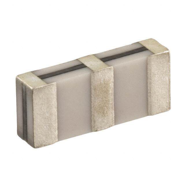
| 产品图片 |
|
| rohs | 符合RoHS无铅 / 符合限制有害物质指令(RoHS)规范要求 |
| 产品系列 | Murata Electronics CFUKF455KB4X-R0CFUKF |
| 数据手册 | |
| 产品型号 | CFUKF455KB4X-R0 |
| 产品 | Ceramic Filters |
| 产品种类 | 信号调节 |
| 其它名称 | 490-7739-6 |
| 商标 | Murata Electronics |
| 商标名 | CERAFIL |
| 封装 | Reel |
| 工作温度范围 | - 20 C to + 80 C |
| 工厂包装数量 | 450 |
| 标准包装 | 1 |
| 类型 | Ceramic Filter |
| 阻抗 | 1 kOhms |
| 频率 | 455 kHz |
| 频率范围 | 455 kHz |


- 商务部:美国ITC正式对集成电路等产品启动337调查
- 曝三星4nm工艺存在良率问题 高通将骁龙8 Gen1或转产台积电
- 太阳诱电将投资9.5亿元在常州建新厂生产MLCC 预计2023年完工
- 英特尔发布欧洲新工厂建设计划 深化IDM 2.0 战略
- 台积电先进制程称霸业界 有大客户加持明年业绩稳了
- 达到5530亿美元!SIA预计今年全球半导体销售额将创下新高
- 英特尔拟将自动驾驶子公司Mobileye上市 估值或超500亿美元
- 三星加码芯片和SET,合并消费电子和移动部门,撤换高东真等 CEO
- 三星电子宣布重大人事变动 还合并消费电子和移动部门
- 海关总署:前11个月进口集成电路产品价值2.52万亿元 增长14.8%
PDF Datasheet 数据手册内容提取
!Note(cid:129) Please read rating and !CAUTION (for storage, operating, rating, soldering, mounting and handling) in this catalog to prevent smoking and/or burning, etc. P05E.pdf (cid:129) This catalog has only typical specifi cations because there is no space for detailed specifi cations. Therefore, please review our product specifi cations or consult the approval sheet for product specifi cations before ordering. Nov.24,2011 r Ceramic Filters (CERAFIL )/ Ceramic Discriminators for Communications Equipment Cat.No.P05E-16
!Note(cid:129) Please read rating and !CAUTION (for storage, operating, rating, soldering, mounting and handling) in this catalog to prevent smoking and/or burning, etc. P05E.pdf (cid:129) This catalog has only typical specifi cations because there is no space for detailed specifi cations. Therefore, please review our product specifi cations or consult the approval sheet for product specifi cations before ordering. Nov.24,2011 EU RoHS Compliant (cid:115) All the products in this catalog comply with EU RoHS. (cid:115) EU RoHS is "the European Directive 2011/65/EU on the Restriction of the Use of Certain Hazardous Substances in Electrical and Electronic Equipment." (cid:115) For more details, please refer to our website 'Murata's Approach for EU RoHS' (http://www.murata.com/info/rohs.html).
!Note(cid:129) Please read rating and !CAUTION (for storage, operating, rating, soldering, mounting and handling) in this catalog to prevent smoking and/or burning, etc. P05E.pdf (cid:129) This catalog has only typical specifi cations because there is no space for detailed specifi cations. Therefore, please review our product specifi cations or consult the approval sheet for product specifi cations before ordering. Nov.24,2011 CONTENTS 1 CERAFILr and "CERAFIL" in this catalog are the trademarks of Murata Manufacturing Co., Ltd. 2 Part Numbering 2 Products Guide 4 3 1 CERAFILr kHz SMD Type SFPKA Series 5 4 2 CERAFILr kHz SMD Type CFUKG Series 7 3 CERAFILr kHz SMD Type CFUKG_X Series 9 5 4 CERAFILr kHz SMD Type CFUKF Series 11 5 CERAFILr kHz SMD Type CFWKA Series 13 6 6 CERAFILr kHz SMD Type CFWKA_Y Series 15 7 kHz SMD Type CERAFILr Notice 17 7 CERAFILr MHz SMD Type SFECF10M7 Series 21 8 8 CERAFILr MHz SMD Type SFSCE10M7 Series 23 MHz SMD Type CERAFILr Notice 25 9 SMD Type CERAFILr Standard Land Pattern Dimensions 31 10 kHz SMD Type CERAFILr Packaging 32 MHz SMD Type CERAFILr Packaging 34 11 9 CERAFILr Plastic Case General Use CFULA Series 35 10 CERAFILr Plastic Case General Use CFWLA Series 37 12 11 CERAFILr Plastic Case Miniaturized Type CFULB Series 39 13 12 CERAFILr Plastic Case Miniaturized Type CFWLB Series 41 13 CERAFILr Plastic Case Group Delay Flat Type CFULA_Y Series 43 14 14 CERAFILr Plastic Case Group Delay Flat Type CFWLA_Y Series 45 15 CERAFILr Plastic Case Group Delay Flat Type Miniaturized Type CFULB_Y Series 47 15 16 CERAFILr Plastic Case Group Delay Flat Type CFWLB_Y Series 49 16 Plastic Case Type CERAFILr Minimum Quantity/Notice 51 17 kHz Type Ceramic Discriminators 52 17 18 MHz Type Ceramic Discriminators 65 Ceramic Discriminators Notice 70 18 Ceramic Discriminators Standard Land Pattern Dimensions/Packaging 74
!Note(cid:129) Please read rating and !CAUTION (for storage, operating, rating, soldering, mounting and handling) in this catalog to prevent smoking and/or burning, etc. P05E.pdf (cid:129) This catalog has only typical specifi cations because there is no space for detailed specifi cations. Therefore, please review our product specifi cations or consult the approval sheet for product specifi cations before ordering. Nov.24,2011 o Part Numbering Ceramic Filters (CERAFILr) for IF (Part Number) SF P KA 455K D4A -R0 SF E CF 10M7 DF00 S0 -R0 q w e r t y u qProduct ID wOscillating/Element tProduct Specification Product ID Oscillating/Element Code Product Specification U 4 Elements Area Expansion mode Three-digit alphanumerics express pass bandwidth, CF D4A W 6 Elements Area Expansion mode center frequency tolerance and design type. Ceramic Filters P 4 Elements Area Expansion mode SFE/S/J series are expressed by four-digit alphanumerics. SF E 2 Elements Thickness Expansion mode S 2 Elements Thickness Shear mode yIndividual Specification Code Individual Specification Code eStructure/Size 001 Expressed by three-digit alphanumerics. Code Structure/Size SFE/S/J series are expressed by two-digit alphanumerics. Cp/Kp Chip Type With standard type, y is omitted. Lp Lead Type p is "A" or subsequent code, which indicates the size. It varies uPackaging depending on vibration mode and number of elements. Code Packaging Chip type is only applied for SF series. -B0 Bulk -R0 Embossed Taping ø=180mm rNominal Center Frequency -R1 Embossed Taping ø=330mm Expressed by four-digit alphanumerics. The unit is hertz (Hz). If Embossed taping is applied to chip type. the unit is "kHz", it is expressed by three figures plus "K." If the unit is "MHz", a decimal point is expressed by the capital letter "M." 2
!Note(cid:129) Please read rating and !CAUTION (for storage, operating, rating, soldering, mounting and handling) in this catalog to prevent smoking and/or burning, etc. P05E.pdf (cid:129) This catalog has only typical specifi cations because there is no space for detailed specifi cations. Therefore, please review our product specifi cations or consult the approval sheet for product specifi cations before ordering. Nov.24,2011 Ceramic Discriminators for IF (kHz) (Part Number) CD B LB 450K C A X 16 -B0 q w e r t y u i o qProduct ID yApplication Product ID Code Application CD Ceramic Discriminators A Standard L Application with coil wOscillating Code Oscillating uElement Type B Area Expansion mode Code Element Type X Low-capacitance eStructure/Size Y High-capacitance Code Structure/Size Cp/Kp Chip Type iIC Lp Lead Type Code IC p is "A" or subsequent code, which indicates the size. It varies 16 Applicable IC Control code depending on vibration mode and number of elements. oPackaging rNominal Center Frequency Code Packaging Expressed by four-digit alphanumerics. The unit is in hertz (Hz). -B0 Bulk Capital letter "K" following three figures expresses the unit of -R0 Embossed Taping ø=180mm "kHz." -R1 Embossed Taping ø=330mm tDetection Embossed taping is applied to chip type. With non-standard products, one letter indicating "Individual Specification" is added between Code Detection "iApplicable IC" and "oPackage Specification code." C Quadrature Detection Ceramic Discriminators for IF (MHz) (Part Number) CD S CB 10M7 GF 001 -R0 q w e r t y u qProduct ID tProduct Specification Product ID Code Product Specification CD Discriminators Two-digit alphanumerics express GF type, center frequency, rank, others wOscillation Code Oscillation yIC S Thickness Shear mode Code IC 001 Applicable IC Control Code eStructure/Size Code Structure/Size uPackaging Cp Chip Type Code Packaging p is expressed "A" or subsequent code, which indicates the size. -R0 Embossed Taping ø=180mm With non-standard products, an alphanumerics indicating "Individual rNominal Center Frequency Specification" is added between "yIC" and "uPackaging." Expressed by four-digit alphanumerics. The unit is in hertz (MHz). Decimal point is expressed by capital letter "M." 3
!Note(cid:129) Please read rating and !CAUTION (for storage, operating, rating, soldering, mounting and handling) in this catalog to prevent smoking and/or burning, etc. P05E.pdf (cid:129) This catalog has only typical specifi cations because there is no space for detailed specifi cations. Therefore, please review our product specifi cations or consult the approval sheet for product specifi cations before ordering. Nov.24,2011 Products Guide oSMD Type (kHz) Applications General Use Attenuation Type 6dB Bandwidth (kHz) min. (dB) min. Series A B C D E F G H J K L ±17.5 ±15 ±12.5 ±10 ±7.5 ±6 ±4.5 ±3 ±2 ±1.5 ±1 Within 455±80 or ±100kHz SFPKA455KM High Selectivity (4 Elements) – – – o o o o o – – – 27 (G to H; 25) Series (Plastic Case Type) CFUKG455KM – – – o o o o – – – – 27 (G; 25) (4 Elements) Narrow Bandwidth GDT Flat Type CFUKG455KMX – – – – o o o o – – – 27 (G to H; 25) Miniature Series (4 Elements) (Plastic Case Type) GDT Flat Type CFUKF455KM Miniature Series o o o o o – – – – – – 25 (D to E; 23) (4 Elements) (Plastic Case Type) GDT Flat Type High Selectivity CFWKA450KBFY – o – – – – – – – – – 45 SMD Series (6 Elements) (Plastic Case Type) High Selectivity CFWKA450KM SMD Series – – – o o o o – – – – 50 (6 Elements) (Plastic Case Type) oLead Type (kHz) Applications General Use Attenuation Type 6dB Bandwidth (kHz) min. (dB) min. Series A B C D E F G H J K L ±17.5 ±15 ±12.5 ±10 ±7.5 ±6 ±4.5 ±3 ±2 ±1.5 ±1 Within 455±80 or ±100kHz High Selectivity CFULA455KM (4 Elements) – o o o o o o o – – – 27((GH;; 3255)) Low Profile Series CFWLA455KM (6 Elements) – o o o o o o o o – – 35 (H, J; 60) High Selectivity CFULB455KM (4 Elements) – o o o o o o o o – – 27((GH,; J2;5 3)5) Miniature Series CFWLB455KM (6 Elements) – o o o o o o o o – – 35 (H, J; 55) GDT Flat Type CFULA455KMY (4 Elements) – o o o o o o – – – – 25 (D to G; 23) Series CFWLA455KMY (6 Elements) o o o o o o o – – – – 40 GDT Flat Type CFULB455KMY (4 Elements) – o o o o o o – – – – 25 (D to G; 23) Miniature Series CFWLB455KMY (6 Elements) o o o o o o o – – – – 40 (F; 35) 4
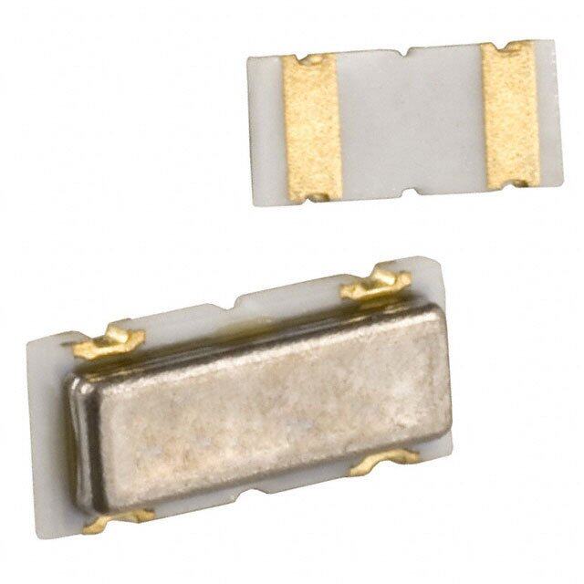
!Note• Please read rating and !CAUTION (for storage, operating, rating, soldering, mounting and handling) in this catalog to prevent smoking and/or burning, etc. P05E.pdf • This catalog has only typical specifi cations because there is no space for detailed specifi cations. Therefore, please review our product specifi cations or consult the approval sheet for product specifi cations before ordering. Nov.24,2011 r Ceramic Filters (CERAFIL ) for Communications Equipment 1 CERAFILr kHz SMD Type SFPKA Series The SFPKA series is comprised of small, high-performance, 7.0±0.3 3.0±0.3 economical, thin (5.0mm) fi lters consisting of 4 ceramic eshlerminekinntgs .m Tohbeiilre i ncnoomvmatuivneic caotinosnt rpurcotdiounc tiss spuecrfhe cats f ocro rdless 7.5±0.3 MARKECINIOADGJE 8.4 max. phones, pagers and transceivers. 0.9±0.1 max. c Features 5.0 1. The fi lters are mountable by automatic placers. 1.5±0.3 2.0±0.3 2.0±0.3 1.5±0.3 1.6±0.3 2. The fi lters can be refl ow soldered and withstand Connection washing. (1) (2) (3) ((12)):: IGnrpouutnd (3): Output 3. They are slim, at only 5.0mm maximum thickness. (in mm) 4. The bandwidth ranges from D to H. 5. Operating temperature range: -20 to +80 (°C) Storage temperature range: -40 to +85 (°C) Center 6dB Stop Stop Band Insertion Loss Ripple Input/Output Part Number Frequency (fo) Bandwidth Bandwidth Attenuation Impedance (kHz) (kHz) (kHz) (dB) (dB) (dB) (ohm) 455 fn±10.0 fn±20.0 max. 27 min. 4.0 max. 2.0 max. SFPKA455KD4A-R1 1500 ±1.5kHz min. [within 40dB] [within fn±100kHz] [at minimum loss point] [within fn±7kHz] 455 fn±7.5 fn±15.0 max. 27 min. 6.0 max. 1.5 max. SFPKA455KE4A-R1 1500 ±1.5kHz min. [within 40dB] [within fn±100kHz] [at minimum loss point] [within fn±5kHz] 455 fn±6.0 fn±12.5 max. 27 min. 6.0 max. 1.5 max. SFPKA455KF4A-R1 1500 ±1.5kHz min. [within 40dB] [within fn±100kHz] [at minimum loss point] [within fn±4kHz] 455 fn±4.5 fn±10.0 max. 25 min. 6.0 max. 1.5 max. SFPKA455KG1A-R1 1500 ±1.0kHz min. [within 40dB] [within fn±100kHz] [at minimum loss point] [within fn±3kHz] 455 fn±3.0 fn±9.0 max. 35 min. 6.0 max. 1.5 max. SFPKA455KH1A-R1 2000 ±1.0kHz min. [within 40dB] [within fn±100kHz] [at minimum loss point] [within fn±2kHz] Center frequency (fo) defi ned by the center of 6dB bandwidth. (fn) means nominal center frequency 455kHz. For safety purposes, connect the output of fi lters to the IF amplifi er through a DC blocking capacitor. Avoid applying a direct current to the output of ceramic fi lters. The order quantity should be an integral multiple of the "Minimum Quantity" shown in package page in this catalog. c Test Circuit R1 (1) (3) (2) RF Voltmeter Rg E1 R2 E2 S.S.G. 0dBm (1): Input Rg+R1=R2=Input/Output Impedance (2): Ground E1: S.S.G. Output Voltage (3): Output 5
!Note(cid:129) Please read rating and !CAUTION (for storage, operating, rating, soldering, mounting and handling) in this catalog to prevent smoking and/or burning, etc. P05E.pdf (cid:129) This catalog has only typical specifi cations because there is no space for detailed specifi cations. Therefore, please review our product specifi cations or consult the approval sheet for product specifi cations before ordering. Nov.24,2011 c Frequency Characteristics 1 SFPKA455KE4A-R1 SFPKA455KE4A-R1 0 400 0 10 360 10 20 320 20 30 280 30 Attenuation (dB) 465000 212460000 G.D.T. (μsec.) Attenuation (dB) 465000 70 120 70 80 80 80 90 40 90 100 430 455 480 0 102000 300 400 500 600 700 800 900 1000 Frequency (kHz) Frequency (kHz) 6
!Note(cid:129) Please read rating and !CAUTION (for storage, operating, rating, soldering, mounting and handling) in this catalog to prevent smoking and/or burning, etc. P05E.pdf (cid:129) This catalog has only typical specifi cations because there is no space for detailed specifi cations. Therefore, please review our product specifi cations or consult the approval sheet for product specifi cations before ordering. Nov.24,2011 r Ceramic Filters (CERAFIL ) for Communications Equipment CERAFILr kHz SMD Type CFUKG Series 2 The CFUKG series is comprised of small, high-performance, tThhine i(r4 in.0nmomva)t ifiv lete crso ncsotnruscisttioinng iso fp 4e rcfeercat mfoirc sehlerimnkeinngts. 6.5±0.3 MARKIENIAGJ 7.5 max. CODE mobile communication products such as pocket pagers 1.0±0.1 1.0±0.1 C0.5 1.2±0.1 and cellular phones. max. c Features 4.0 1.0±0.3 4.0±0.3 1.0±0.3 1. The fi lters are mountable by automatic placers. 6.0±0.3 1.5±0.3 1.5±0.3 3.0±0.3 2. The fi lters can be refl ow soldered and withstand Connection washing. (1) (2) ((12)):: IOnuptuptut (3): Ground 3. They are slim, at only 4.0mm maximum thickness, (3) and have a small mounting area (7.5x6.0mm) (in mm) enabling fl exible PCB design. 4. The bandwidth ranges from D to G. 5. Operating temperature range: -20 to +80 (°C) Storage temperature range: -40 to +85 (°C) Center 6dB Stop Stop Band Insertion Loss Ripple Input/Output Part Number Frequency (fo) Bandwidth Bandwidth Attenuation Impedance (kHz) (kHz) (kHz) (dB) (dB) (dB) (ohm) 455 fn±10.0 fn±20.0 max. 27 min. 4.0 max. 2.0 max. CFUKG455KD4A-R0 1500 ±1.5kHz min. [within 40dB] [within fn±100kHz] [at minimum loss point] [within fn±7kHz] 455 fn±7.5 fn±15.0 max. 27 min. 6.0 max. 1.5 max. CFUKG455KE4A-R0 1500 ±1.5kHz min. [within 40dB] [within fn±100kHz] [at minimum loss point] [within fn±5kHz] 455 fn±6.0 fn±12.5 max. 27 min. 6.0 max. 1.5 max. CFUKG455KF4A-R0 1500 ±1.5kHz min. [within 40dB] [within fn±100kHz] [at minimum loss point] [within fn±4kHz] 455 fn±4.5 fn±10.0 max. 25 min. 6.0 max. 1.5 max. CFUKG455KG1A-R0 1500 ±1.0kHz min. [within 40dB] [within fn±100kHz] [at minimum loss point] [within fn±3kHz] Center frequency (fo) defi ned by the center of 6dB bandwidth. (fn) means nominal center frequency 455kHz. For safety purposes, connect the output of fi lters to the IF amplifi er through a DC blocking capacitor. Avoid applying a direct current to the output of ceramic fi lters. The order quantity should be an integral multiple of the "Minimum Quantity" shown in package page in this catalog. c Test Circuit R1 (1) (2) Rg E1 R2 E2 RF Voltmeter S.S.G. (3) Connection 0dBm (1): Input (2): Output (3): Ground Rg+R1=R2=Input/Output Impedance 7
!Note(cid:129) Please read rating and !CAUTION (for storage, operating, rating, soldering, mounting and handling) in this catalog to prevent smoking and/or burning, etc. P05E.pdf (cid:129) This catalog has only typical specifi cations because there is no space for detailed specifi cations. Therefore, please review our product specifi cations or consult the approval sheet for product specifi cations before ordering. Nov.24,2011 c Frequency Characteristics CFUKG455KE4A-R0 CFUKG455KE4A-R0 0 400 0 2 10 10 20 20 300 30 30 Attenuation (dB) 465000 200 G.D.T. (μsec.) Attenuation (dB) 465000 70 70 100 80 80 90 90 100 0 100 430 455 480 200 300 400 500 600 700 800 900 1000 Frequency (kHz) Frequency (kHz) 8
!Note(cid:129) Please read rating and !CAUTION (for storage, operating, rating, soldering, mounting and handling) in this catalog to prevent smoking and/or burning, etc. P05E.pdf (cid:129) This catalog has only typical specifi cations because there is no space for detailed specifi cations. Therefore, please review our product specifi cations or consult the approval sheet for product specifi cations before ordering. Nov.24,2011 r Ceramic Filters (CERAFIL ) for Communications Equipment CERAFILr kHz SMD Type CFUKG_X Series 3 The CFUKG_X series is comprised of small, high- pceerrafomrmica enlecem, ethnitns .(4.0mm) fi lters consisting of 4 6.5±0.3 MARKIENIAGJ 7.5 max. CODE The fi lters exhibit an extremely fl at GDT 1.0±0.1 1.0±0.1 C0.5 1.2±0.1 characteristic combined with a narrow bandwidth. The fi lters are recommended for narrow band digital max. communication applications. 4.0 1.0±0.3 4.0±0.3 1.0±0.3 6.0±0.3 1.5±0.3 1.5±0.3 3.0±0.3 c Features Connection 1. The fi lters are mountable by automatic placers. (1) (2) ((12)):: IOnuptuptut (3): Ground 2. The fi lters can be refl ow soldered and withstand (3) washing. (in mm) 3. They are slim, at only 4.0mm maximum thickness, and have a small mounting area (7.5x6.0mm) enabling fl exible PCB design. 4. The bandwidth ranges from E to H. 5. Operating temperature range: -20 to +80 (°C) Storage temperature range: -40 to +85 (°C) Center 6dB Stop Stop Band Insertion Loss Ripple GDT Deviation Input/Output Part Number Frequency (fo) Bandwidth Bandwidth Attenuation Impedance (kHz) (kHz) (kHz) (dB) (dB) (dB) (µs) (ohm) 455 fn±7.5 fn±17.5 max. 27 min. 6.0 max. 1.0 max. 25.0 max. CFUKG455KE4X-R0 1500 ±1.5kHz min. [within 40dB] [within fn±100kHz] [at minimum loss point] [within fn±5kHz] [within fn±5kHz] 455 fn±6.0 fn±15.0 max. 27 min. 6.0 max. 1.0 max. 25.0 max. CFUKG455KF4X-R0 1500 ±1.5kHz min. [within 40dB] [within fn±100kHz] [at minimum loss point] [within fn±4kHz] [within fn±4kHz] 455 fn±4.5 fn±12.5 max. 25 min. 6.0 max. 1.0 max. 25.0 max. CFUKG455KG1X-R0 1500 ±1.0kHz min. [within 40dB] [within fn±100kHz] [at minimum loss point] [within fn±3kHz] [within fn±3kHz] 455 fn±3.0 fn±10.0 max. 25 min. 7.0 max. 1.0 max. 25.0 max. CFUKG455KH1X-R0 1500 ±1.0kHz min. [within 40dB] [within fn±100kHz] [at minimum loss point] [within fn±2kHz] [within fn±2kHz] Center frequency (fo) defi ned by the center of 6dB bandwidth. (fn) means nominal center frequency 455kHz. For safety purposes, connect the output of fi lters to the IF amplifi er through a DC blocking capacitor. Avoid applying a direct current to the output of ceramic fi lters. The order quantity should be an integral multiple of the "Minimum Quantity" shown in package page in this catalog. c Test Circuit R1 (1) (2) Rg E1 R2 E2 RF Voltmeter S.S.G. (3) Connection 0dBm (1): Input (2): Output (3): Ground Rg+R1=R2=Input/Output Impedance 9
!Note(cid:129) Please read rating and !CAUTION (for storage, operating, rating, soldering, mounting and handling) in this catalog to prevent smoking and/or burning, etc. P05E.pdf (cid:129) This catalog has only typical specifi cations because there is no space for detailed specifi cations. Therefore, please review our product specifi cations or consult the approval sheet for product specifi cations before ordering. Nov.24,2011 c Frequency Characteristics CFUKG455KE4X-R0 CFUKG455KE4X-R0 0 200 0 10 10 20 20 150 3 30 30 Attenuation (dB) 465000 100 G.D.T. (μsec.) Attenuation (dB) 465000 70 70 50 80 80 90 90 100 0 100 430 455 480 200 300 400 500 600 700 800 900 1000 Frequency (kHz) Frequency (kHz) 10
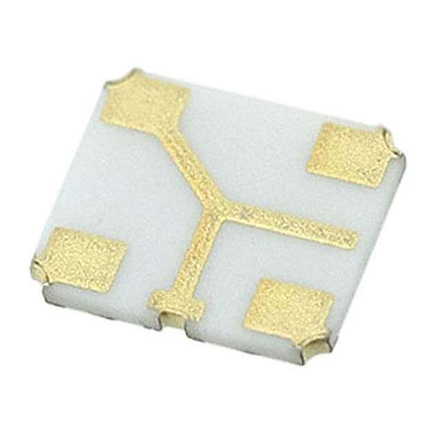
!Note(cid:129) Please read rating and !CAUTION (for storage, operating, rating, soldering, mounting and handling) in this catalog to prevent smoking and/or burning, etc. P05E.pdf (cid:129) This catalog has only typical specifi cations because there is no space for detailed specifi cations. Therefore, please review our product specifi cations or consult the approval sheet for product specifi cations before ordering. Nov.24,2011 r Ceramic Filters (CERAFIL ) for Communications Equipment CERAFILr kHz SMD Type CFUKF Series The CFUKF series is comprised of small, high-performance, tThhine (fi4 lt.e0rms mex) hfi ilbteitr sa nc oenxstrisetminegl yo ffl a4t cGeDraTm ic elements. 6.5±0.3 MARKIECNIOAGDJE 7.5 max. characteristic. 4 1.0±0.1 1.0±0.1 C0.5 1.2±0.1 The fi lters are recommended for digital communication applications and are perfect in hand-held max. cellular phones, etc. 4.0 1.0±0.3 4.0±0.3 1.0±0.3 6.0±0.3 1.5±0.3 1.5±0.3 3.0±0.3 c Features Connection 1. The fi lters are mountable by automatic placers. (1) (2) ((12)):: IOnuptuptut (3): Ground 2. The fi lters can be refl ow soldered and withstand (3) washing. (in mm) 3. They are slim, at only 4.0mm maximum thickness, and have a small mounting area (7.5x6.0mm) enabling fl exible PCB design. 4. The bandwidth ranges from A to E. 5. Operating temperature range: -20 to +80 (°C) Storage temperature range: -40 to +85 (°C) Center 6dB Stop Stop Band Insertion Loss Ripple GDT Deviation Input/Output Part Number Frequency (fo) Bandwidth Bandwidth Attenuation Impedance (kHz) (kHz) (kHz) (dB) (dB) (dB) (µs) (ohm) 455 fn±17.5 fn±40.0 max. 25 min. 4.0 max. 1.0 max. 15.0 max. CFUKF455KA2X-R0 1000 ±2.0kHz min. [within 40dB] [within fn±100kHz] [at minimum loss point] [within fn±12kHz] [within fn±12kHz] 455 fn±15.0 fn±35.0 max. 25 min. 5.0 max. 1.0 max. 15.0 max. CFUKF455KB4X-R0 1000 ±1.5kHz min. [within 40dB] [within fn±100kHz] [at minimum loss point] [within fn±10kHz] [within fn±10kHz] 455 fn±12.5 fn±30.0 max. 25 min. 6.0 max. 1.0 max. 15.0 max. CFUKF455KC4X-R0 1000 ±1.5kHz min. [within 40dB] [within fn±100kHz] [at minimum loss point] [within fn±8kHz] [within fn±8kHz] 455 fn±10.0 fn±25.0 max. 23 min. 7.0 max. 1.0 max. 20.0 max. CFUKF455KD1X-R0 1500 ±1.0kHz min. [within 40dB] [within fn±100kHz] [at minimum loss point] [within fn±7kHz] [within fn±7kHz] 455 fn±7.5 fn±20.0 max. 23 min. 8.0 max. 1.0 max. 20.0 max. CFUKF455KE1X-R0 1500 ±1.0kHz min. [within 40dB] [within fn±100kHz] [at minimum loss point] [within fn±5kHz] [within fn±5kHz] Center frequency (fo) defi ned by the center of 6dB bandwidth. (fn) means nominal center frequency 455kHz. For safety purposes, connect the output of fi lters to the IF amplifi er through a DC blocking capacitor. Avoid applying a direct current to the output of ceramic fi lters. The order quantity should be an integral multiple of the "Minimum Quantity" shown in package page in this catalog. c Test Circuit R1 (1) (2) Rg E1 R2 E2 RF Voltmeter S.S.G. (3) Connection 0dBm (1): Input (2): Output (3): Ground Rg+R1=R2=Input/Output Impedance 11
!Note(cid:129) Please read rating and !CAUTION (for storage, operating, rating, soldering, mounting and handling) in this catalog to prevent smoking and/or burning, etc. P05E.pdf (cid:129) This catalog has only typical specifi cations because there is no space for detailed specifi cations. Therefore, please review our product specifi cations or consult the approval sheet for product specifi cations before ordering. Nov.24,2011 c Frequency Characteristics CFUKF455KE1X-R0 CFUKF455KE1X-R0 0 200 0 10 10 20 20 150 30 30 4 Attenuation (dB) 465000 100 G.D.T. μ(sec.) Attenuation (dB) 465000 70 70 50 80 80 90 90 100 0 100 430 455 480 200 300 400 500 600 700 800 900 1000 Frequency (kHz) Frequency (kHz) 12
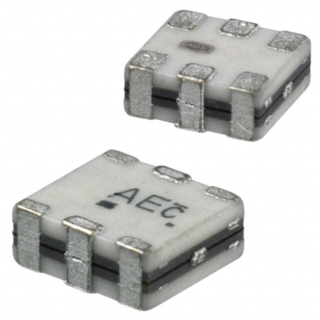
!Note(cid:129) Please read rating and !CAUTION (for storage, operating, rating, soldering, mounting and handling) in this catalog to prevent smoking and/or burning, etc. P05E.pdf (cid:129) This catalog has only typical specifi cations because there is no space for detailed specifi cations. Therefore, please review our product specifi cations or consult the approval sheet for product specifi cations before ordering. Nov.24,2011 r Ceramic Filters (CERAFIL ) for Communications Equipment CERAFILr kHz SMD Type CFWKA Series The CFWKA series is comprised of small, high-performance, tThhine (fi3 lt.e0rms mar)e fi lrteecrso mcomnesnisdti nfogr opfa 6g ecre orar mhaicn edl-ehmelednts. 6.5 MARKECIIONADJGE 7.5 max. Dot marking cellular phones. Sealing 1.2±0.1 1.2±0.1 C0.3 1.2±0.1 1.2±0.1 c Features max. 1. The fi lters are mountable by automatic placers. 3.0 5.5 3.0 3.0 5.5 3.0 5 11.5 1.5±0.3 1.5±0.3Sealing 2. The fi lters can be refl ow soldered. 3. They are slim, at only 3.0mm maximum thickness. (1): Input (1) (2) (2): Output 4. The fi lters are wide bandwidth, fl at GDT within (4) (3) (3)(4): Ground pass band. (Tolerance ±0in.3 mmmm) 5. Operating temperature range: -20 to +80 (°C) Storage temperature range: -40 to +85 (°C) Nominal Center 3dB 6dB Stop Stop Band Stop Band Att.(2) Insertion Loss Ripple Input/Output Part Number Frequency (fn) Bandwidth Bandwidth Bandwidth Attenuation Impedance (kHz) (kHz) (kHz) (kHz) (dB) (dB) (dB) (dB) (ohm) fn±10.0 fn±20.0 max. 50 min. 4.0 max. 3.0 max. CFWKA450KDFA-R0 450.0 - - 1500 min. [within 50dB] [within fn±100kHz] [at minimum loss point] [within fn±7kHz] fn±7.5 fn±15.0 max. 50 min. 6.0 max. 3.0 max. CFWKA450KEFA-R0 450.0 - - 1500 min. [within 50dB] [within fn±100kHz] [at minimum loss point] [within fn±5kHz] fn±6.5 fn±15.0 max. 55 min. 50 min. 4.0 max. 3.0 max. CFWKA450KEFA001-R0 450.0 - 1500 min. [within 50dB] [fn±18 to ±33kHz] [within fn±100kHz] [at fn] [within fn±6.5kHz] fn±6.0 fn±12.5 min. 50 min. 6.0 max. 3.0 max. CFWKA450KFFA-R0 450.0 - - 1500 min. [within 50dB] [within fn±100kHz] [at minimum loss point] [within fn±4kHz] fn±4.5 fn±11.0 max. 50 min. 6.0 max. 2.0 max. CFWKA450KGFA-R0 450.0 - - 1500 min. [within 50dB] [within fn±100kHz] [at minimum loss point] [within fn±3kHz] For safety purposes, connect the output of fi lters to the IF amplifi er through a DC blocking capacitor. Avoid applying a direct current to the output of ceramic fi lters. The order quantity should be an integral multiple of the "Minimum Quantity" shown in package page in this catalog. c Test Circuit R1 (1) (2) Rg E1 (4) (3) R2 E2 RF C Voonlntmecettioenr S.S.G. 0dBm (1): Input (2): Output (3)(4): Ground Rg+R1=R2=Input/Output Impedance 13
!Note(cid:129) Please read rating and !CAUTION (for storage, operating, rating, soldering, mounting and handling) in this catalog to prevent smoking and/or burning, etc. P05E.pdf (cid:129) This catalog has only typical specifi cations because there is no space for detailed specifi cations. Therefore, please review our product specifi cations or consult the approval sheet for product specifi cations before ordering. Nov.24,2011 c Frequency Characteristics CFWKA450KEFA001-R0 CFWKA450KEFA001-R0 0 400 0 4 10 8 20 300 12 30 Attenuation (dB) 122604 200 G.D.T. (μ sec.) Attenuation (dB) 456000 28 70 5 100 32 80 36 90 40 440.0 450.0 460.0 0 100 430 455 480 Frequency (kHz) Frequency (kHz) CFWKA450KEFA001-R0 0 10 20 30 B) 40 d n ( o ati 50 u n e Att 60 70 80 90 100 200 300 400 500 600 700 800 900 1000 Frequency (kHz) 14
!Note(cid:129) Please read rating and !CAUTION (for storage, operating, rating, soldering, mounting and handling) in this catalog to prevent smoking and/or burning, etc. P05E.pdf (cid:129) This catalog has only typical specifi cations because there is no space for detailed specifi cations. Therefore, please review our product specifi cations or consult the approval sheet for product specifi cations before ordering. Nov.24,2011 r Ceramic Filters (CERAFIL ) for Communications Equipment CERAFILr kHz SMD Type CFWKA_Y Series The CFWKA_Y series is comprised of small, high- pceerrafomrmica enlecem, ethnitns .( T3.h0em fim lte) rfis lt earrse creocnosmistminegn odf f6o r 6.5 YBEC5 IO1A0D JE 7.5 max. digital communication applications and are perfect Dot marking Sealing in hand-held cellular phones. 1.2±0.1 1.2±0.1 C0.31.2±0.1 1.2±0.1 max. c Features 3.0 151..55 3.01.53.0 ±0.3 1.5±0.3Sea5lin.5g 3.0 1. The fi lters are mountable by automatic placers, and can be refl ow soldered. ((14)) ((23)) ((12)):: IOnuptuptut 2. They are slim, at only 3.0mm maximum thickness. (3)(4): Ground 6 (Tolerance ±0.3mm) 3. The fi lters are wide bandwidth, fl at GDT within in mm pass band. 4. Operating temperature range: -20 to +80 (°C) Storage temperature range: -40 to +85 (°C) Nominal Center 3dB 6dB Stop Stop Band Insertion Loss Spurious GDT Deviation Input/Output Part Number Frequency (fn) Bandwidth Bandwidth Bandwidth Attenuation Response Impedance (kHz) (kHz) (kHz) (kHz) (dB) (dB) (dB) (µs) (ohm) fn±11.5 fn±13.0 fn±30.0 max. 45 min. 4.0 max. 20 min. 30.0 max. CFWKA450KBFY001-R0 450.0 1000 min. min. [within 50dB] [within fn±100kHz] [at minimum loss point] [within 0.1 to 1.0MHz] [within fn±10kHz] For safety purposes, connect the output of fi lters to the IF amplifi er through a DC blocking capacitor. Avoid applying a direct current to the output of ceramic fi lters. The order quantity should be an integral multiple of the "Minimum Quantity" shown in package page in this catalog. c Test Circuit R1 (1) (2) Rg E1 (4) (3) R2 E2 RF C Voonlntmecettioenr S.S.G. 0dBm (1): Input (2): Output (3)(4): Ground Rg+R1=R2=Input/Output Impedance 15
!Note(cid:129) Please read rating and !CAUTION (for storage, operating, rating, soldering, mounting and handling) in this catalog to prevent smoking and/or burning, etc. P05E.pdf (cid:129) This catalog has only typical specifi cations because there is no space for detailed specifi cations. Therefore, please review our product specifi cations or consult the approval sheet for product specifi cations before ordering. Nov.24,2011 c Frequency Characteristics 0 200 0 2 10 4 20 150 6 30 Attenuation (dB) 11802 100 G.D.T. (μ sec.) Attenuation (dB) 456000 14 70 50 16 80 18 90 20 0 100 420 430 440 450 460 470 480 200 300 400 500 600 700 800 900 1000 6 Frequency (kHz) Frequency (kHz) 16
!Note(cid:129) Please read rating and !CAUTION (for storage, operating, rating, soldering, mounting and handling) in this catalog to prevent smoking and/or burning, etc. P05E.pdf (cid:129) This catalog has only typical specifi cations because there is no space for detailed specifi cations. Therefore, please review our product specifi cations or consult the approval sheet for product specifi cations before ordering. Nov.24,2011 kHz SMD Type CERAFILr Notice c SFPKA/CFUKG/CFUKF Series Notice o Soldering and Mounting 1. Standard Reflow Soldering Conditions (1) Reflow Filter is soldered twice within the following temperature (cid:48)(cid:69)(cid:65)(cid:75) conditions. (260°C max.) 260 C) 230 ure (° (H2e3a0t°inCg) at er Pre-heating mp 100 e (150-180°C) Gradual T Cooling 30 sec. 60-120 sec. (cid:20)(cid:16)(cid:0)(cid:83)(cid:69)(cid:67)(cid:14) 120 sec. min. max. min. (2) Soldering Iron Electrode is directly soldered with the tip of soldering iron at +350±5°C for 3.0±0.5 seconds. (3) Other Do not use strong acidity flux, more than 0.2wt% chlorine content, in reflow soldering. 2. Wash (1) Cleaning Solvent CFC alternatives (HCFC Series), Isopropyl Alcohol (IPA), (cid:55)(cid:65)(cid:84)(cid:69)(cid:82)(cid:0)(cid:8)(cid:36)(cid:69)(cid:77)(cid:73)(cid:78)(cid:69)(cid:82)(cid:65)(cid:76)(cid:73)(cid:90)(cid:69)(cid:68)(cid:0)(cid:55)(cid:65)(cid:84)(cid:69)(cid:82)(cid:9)(cid:12)(cid:0)(cid:35)(cid:76)(cid:69)(cid:65)(cid:78)(cid:73)(cid:78)(cid:71)(cid:0)(cid:55)(cid:65)(cid:84)(cid:69)(cid:82)(cid:0)(cid:51)(cid:79)(cid:76)(cid:85)(cid:84)(cid:73)(cid:79)(cid:78)(cid:0) (Cleanthrough-750H, Pine Alpha 100S), Silicon (cid:8)(cid:52)(cid:69)(cid:67)(cid:72)(cid:78)(cid:79)(cid:67)(cid:65)(cid:82)(cid:69)(cid:0)(cid:38)(cid:50)(cid:55)(cid:9) (2) Cleaning Conditions (cid:115)(cid:0)(cid:41)(cid:77)(cid:77)(cid:69)(cid:82)(cid:83)(cid:73)(cid:79)(cid:78)(cid:0)(cid:55)(cid:65)(cid:83)(cid:72) 2 minutes max. in above solvent at +60°C max. (cid:115)(cid:0)(cid:51)(cid:72)(cid:79)(cid:87)(cid:69)(cid:82)(cid:0)(cid:79)(cid:82)(cid:0)(cid:50)(cid:73)(cid:78)(cid:83)(cid:69)(cid:0)(cid:55)(cid:65)(cid:83)(cid:72) 2 minutes max. in above solvent at +60°C max. (3) Notice (cid:115)(cid:0)(cid:55)(cid:72)(cid:69)(cid:78)(cid:0)(cid:67)(cid:79)(cid:77)(cid:80)(cid:79)(cid:78)(cid:69)(cid:78)(cid:84)(cid:83)(cid:0)(cid:65)(cid:82)(cid:69)(cid:0)(cid:73)(cid:77)(cid:77)(cid:69)(cid:82)(cid:83)(cid:69)(cid:68)(cid:0)(cid:73)(cid:78)(cid:0)(cid:83)(cid:79)(cid:76)(cid:86)(cid:69)(cid:78)(cid:84)(cid:12)(cid:0)(cid:66)(cid:69)(cid:0)(cid:83)(cid:85)(cid:82)(cid:69)(cid:0)(cid:84)(cid:79)(cid:0) maintain the temperature of components below the temperature of solvent. (cid:115)(cid:0)(cid:48)(cid:76)(cid:69)(cid:65)(cid:83)(cid:69)(cid:0)(cid:68)(cid:79)(cid:0)(cid:78)(cid:79)(cid:84)(cid:0)(cid:85)(cid:83)(cid:69)(cid:0)(cid:85)(cid:76)(cid:84)(cid:82)(cid:65)(cid:83)(cid:79)(cid:78)(cid:73)(cid:67)(cid:0)(cid:67)(cid:76)(cid:69)(cid:65)(cid:78)(cid:73)(cid:78)(cid:71)(cid:14) (cid:115)(cid:0)(cid:52)(cid:79)(cid:84)(cid:65)(cid:76)(cid:0)(cid:87)(cid:65)(cid:83)(cid:72)(cid:73)(cid:78)(cid:71)(cid:0)(cid:84)(cid:73)(cid:77)(cid:69)(cid:0)(cid:83)(cid:72)(cid:79)(cid:85)(cid:76)(cid:68)(cid:0)(cid:66)(cid:69)(cid:0)(cid:20)(cid:0)(cid:77)(cid:73)(cid:78)(cid:85)(cid:84)(cid:69)(cid:83)(cid:0)(cid:77)(cid:65)(cid:88)(cid:73)(cid:77)(cid:85)(cid:77)(cid:14) (cid:115)(cid:0)(cid:48)(cid:76)(cid:69)(cid:65)(cid:83)(cid:69)(cid:0)(cid:69)(cid:78)(cid:83)(cid:85)(cid:82)(cid:69)(cid:0)(cid:84)(cid:72)(cid:69)(cid:0)(cid:67)(cid:79)(cid:77)(cid:80)(cid:79)(cid:78)(cid:69)(cid:78)(cid:84)(cid:0)(cid:73)(cid:83)(cid:0)(cid:84)(cid:72)(cid:79)(cid:82)(cid:79)(cid:85)(cid:71)(cid:72)(cid:76)(cid:89)(cid:0)(cid:69)(cid:86)(cid:65)(cid:76)(cid:85)(cid:65)(cid:84)(cid:69)(cid:68)(cid:0)(cid:73)(cid:78)(cid:0) your application circuit. (cid:115)(cid:0)(cid:48)(cid:76)(cid:69)(cid:65)(cid:83)(cid:69)(cid:0)(cid:68)(cid:79)(cid:0)(cid:78)(cid:79)(cid:84)(cid:0)(cid:85)(cid:83)(cid:69)(cid:0)(cid:67)(cid:72)(cid:76)(cid:79)(cid:82)(cid:73)(cid:78)(cid:69)(cid:12)(cid:0)(cid:80)(cid:69)(cid:84)(cid:82)(cid:79)(cid:76)(cid:69)(cid:85)(cid:77)(cid:0)(cid:79)(cid:82)(cid:0)(cid:65)(cid:76)(cid:75)(cid:65)(cid:76)(cid:73)(cid:0)(cid:67)(cid:76)(cid:69)(cid:65)(cid:78)(cid:73)(cid:78)(cid:71)(cid:0) solvent. (cid:115)(cid:0)(cid:41)(cid:70)(cid:0)(cid:89)(cid:79)(cid:85)(cid:0)(cid:80)(cid:76)(cid:65)(cid:78)(cid:0)(cid:84)(cid:79)(cid:0)(cid:85)(cid:83)(cid:69)(cid:0)(cid:65)(cid:78)(cid:89)(cid:0)(cid:79)(cid:84)(cid:72)(cid:69)(cid:82)(cid:0)(cid:84)(cid:89)(cid:80)(cid:69)(cid:83)(cid:0)(cid:79)(cid:70)(cid:0)(cid:83)(cid:79)(cid:76)(cid:86)(cid:69)(cid:78)(cid:84)(cid:83)(cid:12)(cid:0)(cid:80)(cid:76)(cid:69)(cid:65)(cid:83)(cid:69)(cid:0) consult with Murata or Murata representative prior to using. 3. Coating In case of overcoating the component, conditions such as material of resin, cure temperature, and so on should be evaluated well. Continued on the following page. 17
!Note(cid:129) Please read rating and !CAUTION (for storage, operating, rating, soldering, mounting and handling) in this catalog to prevent smoking and/or burning, etc. P05E.pdf (cid:129) This catalog has only typical specifi cations because there is no space for detailed specifi cations. Therefore, please review our product specifi cations or consult the approval sheet for product specifi cations before ordering. Nov.24,2011 kHz SMD Type CERAFILr Notice Continued from the preceding page. o Storage and Operating Conditions 1. Product Storage Condition (2) Please do not put the products directly on the floor Please store the products in a room where the without anything under them to avoid damp places temperature/humidity is stable, and avoid such places and/or dusty places. where there are large temperature changes. Please store (3) Please do not store the products in places such as a the products under the following conditions: damp heated place or any place exposed to direct Temperature: -10 to +40°C sunlight or excessive vibration. Humidity: 15 to 85% R.H. (4) Please use the products immediately after the 2. Expiration Date on Storage package is opened, because the characteristics may Expiration date (shelf life) of the products is six months be reduced in quality and/or be degraded in after delivery under the conditions of a sealed and solderability due to storage under poor condition. unopened package. Please use the products within six (5) Please do not drop the products to avoid cracking of months after delivery. If you store the products for a long ceramic element. time (more than six months), use carefully because 4. Other solderability may be degraded due to storage under poor Please be sure to consult with our sales representative or conditions. engineer whenever the products are to be used in Please confirm solderability and characteristics for the conditions not listed above. products regularly. 3. Notice on Product Storage (1) Please do not store the products in a chemical atmosphere (Acids, Alkali, Bases, Organic gas, Sulfides and so on), because the characteristics may be reduced in quality and may be degraded in solderability due to storage in a chemical atmosphere. o Rating The component may be damaged if excessive mechanical stress is applied. o Handling 1. If the component is cleaned, please confirm that the 3. For safety purposes, connect the output of filters to the IF reliability has not been degraded. amplifier through a D.C. blocking capacitor. Avoid 2. The components, packed in a moisture-proof bag (dry applying a direct current to the output of ceramic filters. pack), are sensitive to moisture. The following treatment is required before applying reflow soldering, to avoid package cracks or reliability degradation caused by thermal stress. When unpacked, store the component in an atmosphere of below 25°C and below 65%R.H., and solder within 48 hours. 18
!Note(cid:129) Please read rating and !CAUTION (for storage, operating, rating, soldering, mounting and handling) in this catalog to prevent smoking and/or burning, etc. P05E.pdf (cid:129) This catalog has only typical specifi cations because there is no space for detailed specifi cations. Therefore, please review our product specifi cations or consult the approval sheet for product specifi cations before ordering. Nov.24,2011 kHz SMD Type CERAFILr Notice c CFWKA Series Notice o Soldering and Mounting 1. Standard Reflow Soldering Conditions (1) Reflow Filter is soldered twice within the following temperature Peak conditions. (260°C max.) 260 C) 230 ure (° (H2e3a0t°inCg) at er Pre-heating mp 100 e (150-180°C) Gradual T Cooling 30 sec. 60-120 sec. 40 sec. 120 sec. min. max. min. (2) Soldering Iron Electrode is directly soldered with the tip of soldering iron at +350±5°C for 3.0±0.5 seconds. (3) Other Do not use strong acidity flux, more than 0.2wt% chlorine content, in reflow soldering. 2. Wash Do not clean or wash the component as it is not hermetically sealed. 3. Coating Do not apply conformal coating onto the component as it's not hermetically sealed. o Storage and Operating Conditions 1. Product Storage Condition Sulfides and so on), because the characteristics may Please store the products in a room where the be reduced in quality and may be degraded in temperature/humidity is stable, and avoid places where solderability due to storage in a chemical atmosphere. there are large temperature changes. Please store the (2) Please do not put the products directly on the floor products under the following conditions: without anything under them to avoid damp places Temperature: -10 to + 40°C and/or dusty places. Humidity: 15 to 85% R.H. (3) Please do not store the products in places such as a 2. Expiration Date on Storage damp heated place or any place exposed to direct Expiration date (shelf life) of the products is six months sunlight or excessive vibration. after delivery under the conditions of a sealed and (4) Please use the products immediately after the unopened package. Please use the products within six package is opened, because the characteristics may months after delivery. If you store the products for a long be reduced in quality and/or be degraded in time (more than six months), use carefully because the solderability due to storage under poor condition. solderability may be degraded due to storage under poor (5) Please do not drop the products to avoid cracking of conditions. ceramic element. Please confirm solderability and characteristics for the 4. Other products regularly. Please be sure to consult with our sales representative or 3. Notice on Product Storage engineer whenever the products are to be used in (1) Please do not store the products in a chemical conditions not listed above. atmosphere (Acids, Alkali, Bases, Organic gas, Continued on the following page. 19
!Note(cid:129) Please read rating and !CAUTION (for storage, operating, rating, soldering, mounting and handling) in this catalog to prevent smoking and/or burning, etc. P05E.pdf (cid:129) This catalog has only typical specifi cations because there is no space for detailed specifi cations. Therefore, please review our product specifi cations or consult the approval sheet for product specifi cations before ordering. Nov.24,2011 kHz SMD Type CERAFILr Notice Continued from the preceding page. o Rating The component may be damaged if excessive mechanical stress is applied. o Handling For safety purposes, connect the output of filters to the IF amplifier through a D.C. blocking capacitor. Avoid applying a direct current to the output of ceramic filters. 20
!Note• Please read rating and !CAUTION (for storage, operating, rating, soldering, mounting and handling) in this catalog to prevent smoking and/or burning, etc. P05E.pdf • This catalog has only typical specifi cations because there is no space for detailed specifi cations. Therefore, please review our product specifi cations or consult the approval sheet for product specifi cations before ordering. Nov.24,2011 r Ceramic Filters (CERAFIL ) for Communications Equipment CERAFILr MHz SMD Type SFECF10M7 Series SFECF10M7 series for FM receivers are small, 3.45±0.2 1.3±0.1 high-performance and super thin (1.4mm max.) fi lters. The piezoelectric element is sandwiched by the Imnaprukte erlectrode 3.1±0.2 ceramics substrate. 0 to 0.4(0.6)(0.6)(0.6)0 to 0.4 They have 1.4mm max. thickness and a small mounting area (3.45x3.1mm). (1.28)(1.28) SFECF series and CDSCB series (MHz Discriminator) 0.3 min.0.3 min. enable customers to make VICS/RKE/TPMS set very thin 0.65±0.30.7±0.3 0.65±0.3 acn dF esmataullr.es 0.85±0.30.85±0.3 ((16(1)).28)(((521)).28(()43)) 0.75±0.3 ((23( )) (((( 5416 ))))):::::: GNIOERnIoerupAo ftucepJuto runMentdnnocenecthtly Code 1. The fi lters are mountable by automatic placers. 0 to 0.35 0 to 0.35 (in mm) 2. They are slim, at only 1.4mm max. thickness, and 7 have a small mounting area (3.45x3.1mm) enabling fl exible PCB design. 3. Various bandwidths are available. Select a suitable type in accordance with the desired selectivity. 4. Operating Temperature Range: -20 to +80 (°C)(Standard Type) -40 to +85 (°C)(High-reliability Type) Storage Temperature Range: -40 to +85 (°C)(Standard Type) -55 to +85 (°C)(High-reliability Type) Standard Type Center Nominal Center 3dB Attenuation Insertion Loss Ripple Spurious Spurious Input/Output Part Number Frequency Frequency (fn) Bandwidth Attenuation Attenuation Impedance (fo) (MHz) (MHz) (kHz) (kHz) (dB) (dB) (1) (dB) (2) (dB) (ohm) 10.700 30 min. 30 min. SFECF10M7HA00-R0 - 180 ±40kHz 470 max. 4.0±2.0dB 1.0 max. 330 ±30kHz [within 9MHz to fo] [within fo to 12MHz] 8.0max. 30 min. 25 min. SFECF10M7HF00-R0 - 10.700 fn±25 min. 510 max. 1.0 max. 330 [at fn] [within 9MHz to fn] [within fn to 12MHz] 10.700 30 min. 30 min. SFECF10M7GA00-R0 - 230 ±50kHz 510 max. 3.5±2.0dB 1.0 max. 330 ±30kHz [within 9MHz to fo] [within fo to 12MHz] 8.0max. 30 min. 25 min. SFECF10M7GF00-R0 - 10.700 fn±45 min. 560 max. 1.0 max. 330 [at fn] [within 9MHz to fn] [within fn to 12MHz] 10.700 30 min. 30 min. SFECF10M7FA00-R0 - 280 ±50kHz 590 max. 3.0±2.0dB 1.0 max. 330 ±30kHz [within 9MHz to fo] [within fo to 12MHz] 7.0max. 30 min. 25 min. SFECF10M7FF00-R0 - 10.700 fn±65 min. 620 max. 1.0 max. 330 [at fn] [within 9MHz to fn] [within fn to 12MHz] 10.700 30 min. 30 min. SFECF10M7EA00-R0 - 330 ±50kHz 700 max. 3.0±2.0dB 1.0 max. 330 ±30kHz [within 9MHz to fo] [within fo to 12MHz] 10.700 35 min. 25 min. SFECF10M7DA0001-R0 - 420 min. 950 max. 3.0±2.0dB 3.0 max. 330 ±30kHz [within 9MHz to fo] [within fo to 12MHz] 6.0max. 20 min. 20 min. SFECF10M7DF00-R0 - 10.700 fn±150 min. 990 max. 3.0 max. 330 [at fn] [within 9MHz to fn] [within fn to 12MHz] Area of Attenuation: [within 20dB] Area of Insertion Loss: at minimum loss point Area of Ripple: within 3dB B.W. Center frequency (fo) defi ned by center of 3dB bandwidth. For safety purposes, connect the output of fi lters to the IF amplifi er through a DC blocking capacitor. Avoid applying a direct current to the output of ceramic fi lters. The order quantity should be an integral multiple of the "Minimum Quantity" shown in package page in this catalog. 21
!Note• Please read rating and !CAUTION (for storage, operating, rating, soldering, mounting and handling) in this catalog to prevent smoking and/or burning, etc. P05E.pdf • This catalog has only typical specifi cations because there is no space for detailed specifi cations. Therefore, please review our product specifi cations or consult the approval sheet for product specifi cations before ordering. Nov.24,2011 High-reliability Type Center Nominal Center 3dB Attenuation Insertion Loss Ripple Spurious Spurious Input/Output Part Number Frequency Frequency (fn) Bandwidth Attenuation Attenuation Impedance (fo) (MHz) (MHz) (kHz) (kHz) (dB) (dB) (1) (dB) (2) (dB) (ohm) 10.700 30 min. 30 min. SFECF10M7HA00S0-R0 - 180 ±40kHz 470 max. 4.0±2.0dB 1.0 max. 330 ±30kHz [within 9MHz to fo] [within fo to 12MHz] 8.0max. 30 min. 25 min. SFECF10M7HF00S0-R0 - 10.700 fn±25 min. 510 max. 1.0 max. 330 [at fn] [within 9MHz to fn] [within fn to 12MHz] 10.700 30 min. 30 min. SFECF10M7GA00S0-R0 - 230 ±50kHz 510 max. 3.5±2.0dB 1.0 max. 330 ±30kHz [within 9MHz to fo] [within fo to 12MHz] 8.0max. 30 min. 25 min. SFECF10M7GF00S0-R0 - 10.700 fn±45 min. 560 max. 1.0 max. 330 [at fn] [within 9MHz to fn] [within fn to 12MHz] 10.700 30 min. 30 min. SFECF10M7FA00S0-R0 - 280 ±50kHz 590 max. 3.0±2.0dB 1.0 max. 330 ±30kHz [within 9MHz to fo] [within fo to 12MHz] 7.0max. 30 min. 25 min. SFECF10M7FF00S0-R0 - 10.700 fn±65 min. 630 max. 1.0 max. 330 [at fn] [within 9MHz to fn] [within fn to 12MHz] 10.700 30 min. 30 min. SFECF10M7EA00S0-R0 - 330 ±50kHz 700 max. 3.0±2.0dB 1.0 max. 330 ±30kHz [within 9MHz to fo] [within fo to 12MHz] 6.0max. 20 min. 20 min. SFECF10M7DF00S0-R0 - 10.700 fn±145 min. 990 max. 3.0 max. 330 [at fn] [within 9MHz to fn] [within fn to 12MHz] 7 Area of Attenuation: [within 20dB] Area of Insertion Loss: at minimum loss point Area of Ripple: within 3dB B.W. Center frequency (fo) defi ned by center of 3dB bandwidth. For safety purposes, connect the output of fi lters to the IF amplifi er through a DC blocking capacitor. Avoid applying a direct current to the output of ceramic fi lters. The order quantity should be an integral multiple of the "Minimum Quantity" shown in package page in this catalog. c Test Circuit (3) (4) (2) (5) R1 (1) (6) Rg E1 R2 C2 E2 RVoFltmeter S.S.G. Rg = 50Ω R1 = 280Ω ±5% R2 = 330Ω ±5% C2 = 10 ± 2 pF (Including stray capacitance and Input capacitance (2)((51)):: IGnrpouutnd of RF Volt Meter) (3)(4): No connect E1: S.S.G. Output Voltage (6): Output c Frequency Characteristics SFECF10M7FA00-R0 SFECF10M7FA00-R0 0 7.0 0 1 6.0 10 2 5.0 20 Attenuation (dB) 43 43..00 G.D.T. (μsec.) Attenuation (dB)3400 5 2.0 50 6 1.0 60 7 0.0 70 10.300 10.500 10.700 10.900 11.100 8.700 9.700 10.700 11.700 12.700 Frequency (MHz) Frequency (MHz) 22
!Note• Please read rating and !CAUTION (for storage, operating, rating, soldering, mounting and handling) in this catalog to prevent smoking and/or burning, etc. P05E.pdf • This catalog has only typical specifi cations because there is no space for detailed specifi cations. Therefore, please review our product specifi cations or consult the approval sheet for product specifi cations before ordering. Nov.24,2011 r Ceramic Filters (CERAFIL ) for Communications Equipment CERAFILr MHz SMD Type SFSCE10M7 Series SFSCE series are chip surface mount fi lters available for (1) 4.5 (2) 0.4 3dB bandwidth at 700kHz to 1.3MHz. (more than twice width compared with current types) 3.8 * (3.5) They have 1.0mm max. thickness and small mounting area (3) (4.5x3.8mm). (4) (4.0) max. c Features 1.0 12 .. TThahhveee yfi alate rserms s aalimlrle m, maotou ounnntiltnyag b1 la.e0r mebaym (a 4mu.5taoxxm3. .at8htmiicc mkpn)lae ecsnesar, sba.lnindg (1.8) (4-((R14))0.3) (0.3) ((23)) 0.850.150.3 Tolera((((n*1234c)))):::::e IONGE nuIourpnAo tulCpJuet unsoMtsdnonnetchtly Code otherwise specified: ±0.1 fl exible PCB design. 0.61.1 0.15 ( ): Reference (2.25) (in mm) 3. Available lead (Pb) free solder refl ow. 4. Operating temperature range: -20 to +80 (°C) Storage temperature range: -40 to +85 (°C) 8 c Applications 1. SS digital communication system 2. Digital wireless audio 3. PHS Evolution system 4. RFID Reader Writer 5. RKE Nominal Center 3dB Stop Insertion Loss Ripple Spurious GDT Deviation Input/Output Part Number Frequency (fn) Bandwidth Bandwidth Response Impedance (MHz) (kHz) (MHz) (dB) (dB) (dB) (µs) (ohm) fn±500.0 2.2 max. (Total) 6.0 max. 2.0 max. 30/25 min. 0.6 max. SFSCE10M7WF03-R0 10.700 470 min. [within 20dB] [at minimum loss point] [within 3dB Bandwidth] [within 5.7MHz to fn / fn to 15.7MHz] [within fn±400kHz] fn±400.0 1.8 max. (Total) 6.0 max. 1.5 max. 35/25 min. 0.6 max. SFSCE10M7WF04-R0 10.700 470 min. [within 20dB] [at minimum loss point] [within 3dB Bandwidth] [within 5.7MHz to fn / fn to 15.7MHz] [within fn±325kHz] fn±325.0 1.7 max. (Total) 6.0 max. 1.5 max. 40/30 min. 0.6 max. SFSCE10M7WF05-R0 10.700 470 min. [within 20dB] [at minimum loss point] [within 3dB Bandwidth] [within 5.7MHz to fn / fn to 15.7MHz] [within fn±250kHz] For safety purposes, connect the output of fi lters to the IF amplifi er through a DC blocking capacitor. Avoid applying a direct current to the output of ceramic fi lters. The order quantity should be an integral multiple of the "Minimum Quantity" shown in package page in this catalog. c Test Circuit (4) (3) R1 (1) (2) Rg R2 C2 S.S.G. RF Voltmeter (1): Input (2): Output (3): No Connect (4): Ground R1+Rg=R2=Input/Output Impedance, Rg=50Ω C2=10pF (Including stray capacitance and Input capacitance of RF Voltmeter) E1: S.S.G. Output Voltage 23
!Note(cid:129) Please read rating and !CAUTION (for storage, operating, rating, soldering, mounting and handling) in this catalog to prevent smoking and/or burning, etc. P05E.pdf (cid:129) This catalog has only typical specifi cations because there is no space for detailed specifi cations. Therefore, please review our product specifi cations or consult the approval sheet for product specifi cations before ordering. Nov.24,2011 c Frequency Characteristics SFSCE10M7WF03-R0 SFSCE10M7WF03-R0 0 2.0 0 2 1.6 20 Attenuation (dB) 46 10..28 G.D.T. (μsec.) Attenuation (dB)40 60 8 0.4 10 0.0 80 6.700 8.700 10.700 12.700 14.700 9.500 9.900 10.300 10.700 11.100 11.500 11.900 Frequency (MHz) Frequency (MHz) 8 24
!Note(cid:129) Please read rating and !CAUTION (for storage, operating, rating, soldering, mounting and handling) in this catalog to prevent smoking and/or burning, etc. P05E.pdf (cid:129) This catalog has only typical specifi cations because there is no space for detailed specifi cations. Therefore, please review our product specifi cations or consult the approval sheet for product specifi cations before ordering. Nov.24,2011 MHz SMD Type CERAFILr Notice c SFECF10M7 Series Notice o Soldering and Mounting 1. Standard Reflow Soldering Conditions (1) Reflow Filter is soldered twice within the following temperature Peak conditions. (260°C max.) C) 260 e (° 230 atur Heating per Pre-heating (230°C) m (150-180°C) e 100 T Gradual Cooling 30 sec. 60-120 sec. 40 sec. 120 sec. min. max. min. (2) Soldering Iron Filter is soldered at +350±5°C for 3.0±0.5 seconds. The soldering iron should not touch the filter while soldering. (3) Condition for Placement Machines The component is recommended with placement machines that employ optical placement capabilities. The component might be damaged by excessive mechanical force. Please make sure that you have evaluated by using placement machines before going into mass production. Do not use placement machines that utilize mechanical positioning. Please contact Murata for details beforehand. (4) Other (a) The component may be damaged if excess [Component Direction] mechanical stress is applied to it mounted on the Place the printed circuit board. component (b) Design layout of components on the PC board to lateral to the direction in minimize the stress imposed on the warp or flexure of which stress the board. acts. (c) After installing components, if solder is excessively [Component Layout Close to Board] applied to the circuit board, mechanical stress will cause destruction resistance characteristics to Perforation B Susceptibility to degrade. To prevent this, be extremely careful in stress is in the order of : A>C>B determining shape and dimension before designing A Slit C the circuit board diagram. (d) When the positioning claws and pick-up nozzle are worn, the load is applied to the components while positioning is concentrated on positioning accuracy, etc. Careful checking and maintenance are necessary to prevent unexpected trouble. (e) When correcting components with a soldering iron, the tip of the soldering iron should not directly touch the component. Depending on the soldering conditions, the effective area of terminations may be reduced. Solder containing Ag should be used to prevent the electrode erosion. (f) Do not use strong acidity flux, more than 0.2wt% chlorine content, in reflow soldering. Continued on the following page. 25
!Note(cid:129) Please read rating and !CAUTION (for storage, operating, rating, soldering, mounting and handling) in this catalog to prevent smoking and/or burning, etc. P05E.pdf (cid:129) This catalog has only typical specifi cations because there is no space for detailed specifi cations. Therefore, please review our product specifi cations or consult the approval sheet for product specifi cations before ordering. Nov.24,2011 MHz SMD Type CERAFILr Notice Continued from the preceding page. 2. Wash Do not clean or wash the component as it is not hermetically sealed. 3. Coating In case of overcoating the component, conditions such as material of resin, cure temperature, and so on should be evaluated well. o Storage and Operating Conditions 1. Product Storage Condition (2) Please do not put the products directly on the floor Please store the products in a room where the without anything under them to avoid damp places temperature/humidity is stable, and avoid places where and/or dusty places. there are large temperature changes. Please store the (3) Please do not store the products in places such as a products under the following conditions: damp heated place or any place exposed to direct Temperature: -10 to +40°C sunlight or excessive vibration. Humidity: 15 to 85% R.H. (4) Please use the products immediately after the 2. Expiration Date on Storage package is opened, because the characteristics may Expiration date (shelf life) of the products is six months be reduced in quality and/or be degraded in after delivery under the conditions of a sealed and solderability due to storage under poor condition. unopened package. Please use the products within six (5) Please do not drop the products to avoid cracking of months after delivery. If you store the products for a long ceramic element. time (more than six months), use carefully because 4. Other solderability may be degraded due to storage under poor Please be sure to consult with our sales representative or conditions. engineer whenever the products are to be used in Please confirm solderability and characteristics for the conditions not listed above. products regularly. 3. Notice on Product Storage (1) Please do not store the products in a chemical atmosphere (Acids, Alkali, Bases, Organic gas, Sulfides and so on), because the characteristics may be reduced in quality and may be degraded in solderability due to storage in a chemical atmosphere. o Rating The component may be damaged if excessive mechanical stress is applied. o Handling 1. Accurate test circuit values are required to measure 3. For safety purposes, connect the output of filters to the IF electrical characteristics. Miscorrelation may be caused if amplifier through a D.C. blocking capacitor. Avoid there is any deviation, especially stray capacitance, from applying a direct current to the output of ceramic filters. the test circuit in the specification. 2. The components, packed in a moisture proof bag (dry pack), are sensitive to moisture. The following treatment is required before applying reflow soldering, to avoid reliability degradation caused by thermal stress. When unpacked, store the component in an atmosphere of reflow 30°C and below 60%R.H., and solder within 1 week. 26
!Note(cid:129) Please read rating and !CAUTION (for storage, operating, rating, soldering, mounting and handling) in this catalog to prevent smoking and/or burning, etc. P05E.pdf (cid:129) This catalog has only typical specifi cations because there is no space for detailed specifi cations. Therefore, please review our product specifi cations or consult the approval sheet for product specifi cations before ordering. Nov.24,2011 MHz SMD Type CERAFILr Notice c SFSCE10M7WF03-R0 Notice o Soldering and Mounting 1. Standard Reflow Soldering Conditions (1) Reflow Filter is soldered twice within the following temperature Peak conditions. (240°C max.) 240 C) 230 ure (° (H2e3a0t°inCg) at er Pre-heating mp 100 e (150-180°C) Gradual T Cooling 30 sec. 60-120 sec. 30 sec. 120 sec. min. max. min. (2) Soldering Iron Filter is soldered at +280±5°C for 3.0±0.5 seconds. The soldering iron should not touch the filter while soldering. (3) Condition for Placement Machines The component is recommended with placement machines that employ optical placement capabilities. The component might be damaged by excessive mechanical force. Please make sure that you have evaluated by using placement machines before going into mass production. Do not use placement machines that utilize mechanical positioning. Please contact Murata for details beforehand. (4) Other (a) The component may be damaged if excess [Component Layout Close to Board] mechanical stress is applied to it mounted on the printed circuit board. (b) Design layout of components on the PC board to Susceptibility to Perforation B stress is in the order minimize the stress imposed on the warp or flexure of of : A>C>B the board. A Slit C (c) After installing components, if solder is excessively applied to the circuit board, mechanical stress will cause destruction resistance characteristics to [Component Direction] degrade. To prevent this, be extremely careful in Place the compon- determining shape and dimension before designing ent laterally to the direction in which the circuit board diagram. stress acts. (d) When the positioning claws and pick-up nozzle are worn, the load is applied to the components while positioning is concentrated on positioning accuracy, etc. Careful checking and maintenance are necessary to prevent unexpected trouble. (e) When correcting components with a soldering iron, the tip of the soldering iron should not directly touch the component. (f) Do not use strong acidity flux, more than 0.2wt% chlorine content, in reflow soldering. Continued on the following page. 27
!Note(cid:129) Please read rating and !CAUTION (for storage, operating, rating, soldering, mounting and handling) in this catalog to prevent smoking and/or burning, etc. P05E.pdf (cid:129) This catalog has only typical specifi cations because there is no space for detailed specifi cations. Therefore, please review our product specifi cations or consult the approval sheet for product specifi cations before ordering. Nov.24,2011 MHz SMD Type CERAFILr Notice Continued from the preceding page. 2. Wash Do not clean or wash the component as it is not hermetically sealed. 3. Coating In case of overcoating the component, conditions such as material of resin, cure temperature, and so on should be evaluated well. o Storage and Operating Conditions 1. Product Storage Condition (2) Please do not put the products directly on the floor Please store the products in a room where the without anything under them to avoid damp places temperature/humidity is stable, and avoid places where and/or dusty places. there are large temperature changes. Please store the (3) Please do not store the products in places such as a products under the following conditions: damp heated place or any place exposed to direct Temperature: -10 to + 40°C sunlight or excessive vibration. Humidity: 15 to 85% R.H. (4) Please use the products immediately after the 2. Expiration Date on Storage package is opened, because the characteristics may Expiration date (shelf life) of the products is six months be reduced in quality and/or be degraded in after delivery under the conditions of a sealed and solderability due to storage under poor condition. unopened package. Please use the products within six (5) Please do not drop the products to avoid cracking of months after delivery. If you store the products for a long ceramic element. time (more than six months), use carefully because 4. Other solderability may be degraded due to storage under poor Please be sure to consult with our sales representative or conditions. engineer whenever the products are to be used in Please confirm solderability and characteristics for the conditions not listed above. products regularly. 3. Notice on Product Storage (1) Please do not store the products in a chemical atmosphere (Acids, Alkali, Bases, Organic gas, Sulfides and so on), because the characteristics may be reduced in quality and may be degraded in solderability due to storage in a chemical atmosphere. o Rating The component may be damaged if excessive mechanical stress is applied. o Handling 1. Accurate test circuit values are required to measure electrical characteristics. Miscorrelation may be caused if there is any deviation, especially stray capacitance, from the test circuit in the specification. 2. For safety purposes, connect the output of filters to the IF amplifier through a D.C. blocking capacitor. Avoid applying a direct current to the output of ceramic filters. 28
!Note(cid:129) Please read rating and !CAUTION (for storage, operating, rating, soldering, mounting and handling) in this catalog to prevent smoking and/or burning, etc. P05E.pdf (cid:129) This catalog has only typical specifi cations because there is no space for detailed specifi cations. Therefore, please review our product specifi cations or consult the approval sheet for product specifi cations before ordering. Nov.24,2011 MHz SMD Type CERAFILr Notice c SFSCE10M7WF04/05-R0 Notice o Soldering and Mounting 1. Standard Reflow Soldering Conditions (1) Reflow Filter is soldered twice within the following temperature Peak conditions. (260°C max.) 260 C) 230 ure (° (H2e3a0t°inCg) at er Pre-heating mp 100 e (150-180°C) Gradual T Cooling 30 sec. 60-120 sec. 40 sec. 120 sec. min. max. min. (2) Soldering Iron Filter is soldered at +280±5°C for 3.0±0.5 seconds. The soldering iron should not touch the filter while soldering. (3) Condition for Placement Machines The component is recommended with placement machines that employ optical placement capabilities. The component might be damaged by excessive mechanical force. Please make sure that you have evaluated by using placement machines before going into mass production. Do not use placement machines that utilize mechanical positioning. Please contact Murata for details beforehand. (4) Other (a) The component may be damaged if excess [Component Layout Close to Board] mechanical stress is applied to it mounted on the printed circuit board. (b) Design layout of components on the PC board to Susceptibility to Perforation B stress is in the order minimize the stress imposed on the warp or flexure of of : A>C>B the board. A Slit C (c) After installing components, if solder is excessively applied to the circuit board, mechanical stress will cause destruction resistance characteristics to [Component Direction] degrade. To prevent this, be extremely careful in Place the compon- determining shape and dimension before designing ent laterally to the direction in which the circuit board diagram. stress acts. (d) When the positioning claws and pick-up nozzle are worn, the load is applied to the components while positioning is concentrated on positioning accuracy, etc. Careful checking and maintenance are necessary to prevent unexpected trouble. (e) When correcting components with a soldering iron, the tip of the soldering iron should not directly touch the component. (f) Do not use strong acidity flux, more than 0.2wt% chlorine content, in reflow soldering. Continued on the following page. 29
!Note(cid:129) Please read rating and !CAUTION (for storage, operating, rating, soldering, mounting and handling) in this catalog to prevent smoking and/or burning, etc. P05E.pdf (cid:129) This catalog has only typical specifi cations because there is no space for detailed specifi cations. Therefore, please review our product specifi cations or consult the approval sheet for product specifi cations before ordering. Nov.24,2011 MHz SMD Type CERAFILr Notice Continued from the preceding page. 2. Wash Do not clean or wash the component as it is not hermetically sealed. 3. Coating In case of overcoating the component, conditions such as material of resin, cure temperature, and so on should be evaluated well. o Storage and Operating Conditions 1. Product Storage Condition (2) Please do not put the products directly on the floor Please store the products in a room where the without anything under them to avoid damp places temperature/humidity is stable, and avoid places where and/or dusty places. there are large temperature changes. Please store the (3) Please do not store the products in places such as a products under the following conditions: damp heated place or any place exposed to direct Temperature: -10 to + 40°C sunlight or excessive vibration. Humidity: 15 to 85% R.H. (4) Please use the products immediately after the 2. Expiration Date on Storage package is opened, because the characteristics may Expiration date (shelf life) of the products is six months be reduced in quality and/or be degraded in after delivery under the conditions of a sealed and solderability due to storage under poor condition. unopened package. Please use the products within six (5) Please do not drop the products to avoid cracking of months after delivery. If you store the products for a long ceramic element. time (more than six months), use carefully because 4. Other solderability may be degraded due to storage under poor Please be sure to consult with our sales representative or conditions. engineer whenever the products are to be used in Please confirm solderability and characteristics for the conditions not listed above. products regularly. 3. Notice on Product Storage (1) Please do not store the products in a chemical atmosphere (Acids, Alkali, Bases, Organic gas, Sulfides and so on), because the characteristics may be reduced in quality and may be degraded in solderability due to storage in a chemical atmosphere. o Rating The component may be damaged if excessive mechanical stress is applied. o Handling 1. Accurate test circuit values are required to measure electrical characteristics. Miscorrelation may be caused if there is any deviation, especially stray capacitance, from the test circuit in the specification. 2. For safety purposes, connect the output of filters to the IF amplifier through a D.C. blocking capacitor. Avoid applying a direct current to the output of ceramic filters. 30
!Note(cid:129) Please read rating and !CAUTION (for storage, operating, rating, soldering, mounting and handling) in this catalog to prevent smoking and/or burning, etc. P05E.pdf (cid:129) This catalog has only typical specifi cations because there is no space for detailed specifi cations. Therefore, please review our product specifi cations or consult the approval sheet for product specifi cations before ordering. Nov.24,2011 SMD Type CERAFILr Standard Land Pattern Dimensions c SFPKA Series c CFUKG/CFUKF Series 0.7 0.7 6.95 1.2 1.4 1.2 2.475 2.0 0.8 1.6 2.0 7.45 3.5 1.55 0.925 1.21.0 2.0 0.9 2.0 (in mm) (in mm) c CFWKA Series c SFECF10M7 Series 0.1 11.5 0.3 3.0 1.2 5.5 3.0 (6) (5) (4)0.1 1.05 0.3 1.40 0.1 4-R3.0 6.57.5 0.3 (1) (2) (3)0.1 1.05 1.6 2.1 0.1 0.1 (1): Input (2)(5): Ground 0.5 1.8 (in mm) 0.8 0.6 0.8 0.6 0.8 (3)((46)):: NOou tcpountnect It shows solder resist land pattern. (in mm) c SFSCE10M Series 1.05 1.4 0.1 0.1 (3) (4)0.1 1.3 0.8 1.15 0.5 (2) (1) 0.5 (1): Input (2): Output (3): No Connect (4): Ground It shows solder resist land pattern. (in mm) 31
!Note(cid:129) Please read rating and !CAUTION (for storage, operating, rating, soldering, mounting and handling) in this catalog to prevent smoking and/or burning, etc. P05E.pdf (cid:129) This catalog has only typical specifi cations because there is no space for detailed specifi cations. Therefore, please review our product specifi cations or consult the approval sheet for product specifi cations before ordering. Nov.24,2011 kHz SMD Type CERAFILr Packaging c Minimum Quantity Part Number ø180mm ø330mm SFPKA 1,000 CFUKG 450 CFUKF 450 CFWKA 350 c SFPKA Series Dimensions of Carrier Tape Dimensions of Reel 1 Trailer Leader 4.0±0.1 +0.1 ±0. 160 to 190 Cover film 2.0±0.1 ø1.5 -0 75 1. Empty Components Empty 1 240 to 280 5±0. 0.2 1 ø13.0±0.2 400 to 560 7. 16.0± 8.8±0. 80±1 330±2 2.2±0.5 12.0±0.1 User direction of feed 5.3±0.1 Cover film 17.5±0.5 Label 21.5±1.0 7.4±0.1 (cid:115)(cid:0)(cid:48)(cid:65)(cid:82)(cid:84)(cid:0)(cid:78)(cid:85)(cid:77)(cid:66)(cid:69)(cid:82)(cid:0)(cid:77)(cid:65)(cid:82)(cid:75)(cid:69)(cid:68)(cid:0)(cid:83)(cid:73)(cid:68)(cid:69)(cid:0)(cid:73)(cid:83)(cid:0)(cid:65)(cid:76)(cid:87)(cid:65)(cid:89)(cid:83)(cid:0)(cid:70)(cid:65)(cid:67)(cid:73)(cid:78)(cid:71)(cid:0)(cid:85)(cid:80)(cid:14) (in mm) c CFUKG/CFUKF Series Dimensions of Carrier Tape Dimensions of Reel Trailer 2.0±0.1 4.0±0.1 ±0.1 160 to 190 LeadCerover film ø1.5+-00..01 1.75 Empty Components Empty 160 to 200 1 2.0±0.2 7.5±0.6±0.1 16.0±0.2 8.1±0.1 7.7±0.1 +1.0(ø60 )-0 +0(ø180 )-3.0 ø13.0±0.5 400 to 560 7 6. 8.0±0.1 (cid:53)(cid:83)(cid:69)(cid:82)(cid:0)(cid:68)(cid:73)(cid:82)(cid:69)(cid:67)(cid:84)(cid:73)(cid:79)(cid:78)(cid:0)(cid:79)(cid:70)(cid:0)(cid:70)(cid:69)(cid:69)(cid:68) 4.2±0.1 17.0±1.0 19.4±0.3 6.7±0.1 Cover film 6.3±0.1 (cid:115)(cid:0)(cid:48)(cid:65)(cid:82)(cid:84)(cid:0)(cid:78)(cid:85)(cid:77)(cid:66)(cid:69)(cid:82)(cid:0)(cid:77)(cid:65)(cid:82)(cid:75)(cid:69)(cid:68)(cid:0)(cid:83)(cid:73)(cid:68)(cid:69)(cid:0)(cid:73)(cid:83)(cid:0)(cid:65)(cid:76)(cid:87)(cid:65)(cid:89)(cid:83)(cid:0)(cid:70)(cid:65)(cid:67)(cid:73)(cid:78)(cid:71)(cid:0)(cid:85)(cid:80)(cid:14) (in mm) Continued on the following page. 32
!Note(cid:129) Please read rating and !CAUTION (for storage, operating, rating, soldering, mounting and handling) in this catalog to prevent smoking and/or burning, etc. P05E.pdf (cid:129) This catalog has only typical specifi cations because there is no space for detailed specifi cations. Therefore, please review our product specifi cations or consult the approval sheet for product specifi cations before ordering. Nov.24,2011 kHz SMD Type CERAFILr Packaging Continued from the preceding page. c CFWKA Series Dimensions of Carrier Tape Dimensions of Reel Trailer 2.0±0.1 4.0±0.1 ±0.1 160 to 190 LeadCerover film ø1.5+-00..01 75 1. Empty Components Empty 240 to 280 2.0±0.2 11.5±0.1 24.0±0.3 12.4±0.1 12.0±0.1 (ø62.0±1.0) (ø178±2.0) ø13.0±0.5 400 to 560 25.5±1.0 0.4±0.1 29.9±1.0 3.2±0.1 12.0±0.1 User direction of feed 8.1±0.1 Cover film 7.7±0.1 (cid:115)(cid:0)(cid:48)(cid:65)(cid:82)(cid:84)(cid:0)(cid:78)(cid:85)(cid:77)(cid:66)(cid:69)(cid:82)(cid:0)(cid:77)(cid:65)(cid:82)(cid:75)(cid:69)(cid:68)(cid:0)(cid:83)(cid:73)(cid:68)(cid:69)(cid:0)(cid:73)(cid:83)(cid:0)(cid:65)(cid:76)(cid:87)(cid:65)(cid:89)(cid:83)(cid:0)(cid:70)(cid:65)(cid:67)(cid:73)(cid:78)(cid:71)(cid:0)(cid:85)(cid:80)(cid:14) (in mm) 33
!Note(cid:129) Please read rating and !CAUTION (for storage, operating, rating, soldering, mounting and handling) in this catalog to prevent smoking and/or burning, etc. P05E.pdf (cid:129) This catalog has only typical specifi cations because there is no space for detailed specifi cations. Therefore, please review our product specifi cations or consult the approval sheet for product specifi cations before ordering. Nov.24,2011 MHz SMD Type CERAFILr Packaging c Minimum Quantity Part Number ø180mm SFECF 2,000 SFSCE 1,500 c SFECF10M7 Series Dimensions of Carrier Tape Dimensions of Reel Trailer Leader 4.0±0.1 0.1 160 to 190 Cover film ± ø1.55±0.05 2.0±0.05 Chip filter 1.75 x. Empty Components 24E0m top t2y80 a 4.1±0.1 5.5±0.05 12.0±0.2 3° m +1.060-0+0180-1.5 ø13.0±0.5 400 to 560 1 2.0±0.5 0. CP(o0ev.1ee lrit nofig l0m s.7trNe)ngth 10° max. 4.0±0.1 (33°.)35+-00..015 0.3±0.05 (0.05) 1.84±0.1 4.1± 1173..00±+-011..00 User direction of feed (cid:115)(cid:0)(cid:48)(cid:65)(cid:82)(cid:84)(cid:0)(cid:78)(cid:85)(cid:77)(cid:66)(cid:69)(cid:82)(cid:0)(cid:77)(cid:65)(cid:82)(cid:75)(cid:69)(cid:68)(cid:0)(cid:83)(cid:73)(cid:68)(cid:69)(cid:0)(cid:73)(cid:83)(cid:0)(cid:65)(cid:76)(cid:87)(cid:65)(cid:89)(cid:83)(cid:0)(cid:70)(cid:65)(cid:67)(cid:73)(cid:78)(cid:71)(cid:0)(cid:85)(cid:80)(cid:14) ( ): Reference (in mm) c SFSCE10M7 Series Dimensions of Carrier Tape Dimensions of Reel (cid:17) Trailer (cid:44)(cid:69)(cid:65)(cid:68)(cid:69)(cid:82) ±(cid:16)(cid:14) (cid:20)(cid:14)(cid:16)±(cid:16)(cid:14)(cid:17) (cid:17)(cid:22)(cid:16)(cid:0)(cid:84)(cid:79)(cid:0)(cid:17)(cid:25)(cid:16) Cover film (cid:23)(cid:21) (cid:18)(cid:14)(cid:16)±(cid:16)(cid:14)(cid:16)(cid:21) (cid:146)(cid:17)(cid:14)(cid:21)(cid:21)±(cid:16)(cid:14)(cid:16)(cid:21) (cid:16)(cid:14)(cid:19)±(cid:16)(cid:14)(cid:16)(cid:21) (cid:17)(cid:14) (cid:88)(cid:14) (cid:37)(cid:77)(cid:80)(cid:84)(cid:89) (cid:35)(cid:79)(cid:77)(cid:80)(cid:79)(cid:78)(cid:69)(cid:78)(cid:84)(cid:83) (cid:37)(cid:77)(cid:80)(cid:84)(cid:89) (cid:65) (cid:18)(cid:20)(cid:16)(cid:0)(cid:84)(cid:79)(cid:0)(cid:18)(cid:24)(cid:16) (cid:21) (cid:77) ±(cid:17)(cid:18)(cid:14)(cid:16)(cid:16)(cid:14)(cid:18)±(cid:21)(cid:14)(cid:21)(cid:16)(cid:14)(cid:16) (cid:19)(cid:160)(cid:0)±(cid:21)(cid:14)(cid:16)(cid:16)(cid:14)(cid:17) (cid:11)(cid:16)(cid:24)(cid:16)(cid:13)(cid:17)(cid:14)(cid:21) (cid:146)(cid:17)(cid:19)(cid:14)(cid:16)±(cid:16)(cid:14)(cid:21) (cid:20)(cid:16)(cid:16)(cid:0)(cid:84)(cid:79)(cid:0)(cid:21)(cid:22)(cid:16) (cid:17) (cid:17)(cid:14)(cid:17)±(cid:16)(cid:14)(cid:17) (cid:18)(cid:14)(cid:16)±(cid:16)(cid:14)(cid:21) (cid:24)(cid:14)(cid:16)±(cid:16)(cid:14)(cid:17) (cid:146)(cid:17)(cid:14)(cid:21)(cid:21)±(cid:16)(cid:14)(cid:16)(cid:21) Cover film (cid:20)(cid:14)(cid:19)±(cid:16)(cid:14)(cid:17)(cid:48)(cid:16)(cid:14)(cid:69)(cid:17)((cid:69)3(cid:0)(cid:84)(cid:76)°(cid:79)(cid:73)(cid:78))(cid:0)(cid:71)(cid:16)(cid:0)(cid:14)(cid:83)(cid:23)(cid:84)(cid:46)(cid:17)(cid:82)(cid:69)(cid:16)(cid:78)(cid:160)(cid:0)(cid:71)(cid:77)(cid:84)(cid:72)(cid:65)(cid:88)(cid:14) (cid:16)(cid:14)(cid:16)(cid:21)±(cid:16)(cid:14)(cid:19)(cid:16)(cid:14)(cid:16)(cid:21) (cid:17)(cid:17)(cid:23)(cid:19)(cid:14)(cid:14)(cid:16)(cid:16)±(cid:11)(cid:13)(cid:16)(cid:17)(cid:17)(cid:14)(cid:14)(cid:16)(cid:16) (cid:53)(cid:83)(cid:69)(cid:82)(cid:0)(cid:68)(cid:73)(cid:82)(cid:69)(cid:67)(cid:84)(cid:73)(cid:79)(cid:78)(cid:0)(cid:79)(cid:70)(cid:0)(cid:70)(cid:69)(cid:69)(cid:68) (cid:115)(cid:0)(cid:48)(cid:65)(cid:82)(cid:84)(cid:0)(cid:46)(cid:85)(cid:77)(cid:66)(cid:69)(cid:82)(cid:0)(cid:77)(cid:65)(cid:82)(cid:75)(cid:69)(cid:68)(cid:0)(cid:83)(cid:73)(cid:68)(cid:69)(cid:0)(cid:73)(cid:83)(cid:0)(cid:65)(cid:76)(cid:87)(cid:65)(cid:89)(cid:83)(cid:0)(cid:70)(cid:65)(cid:67)(cid:73)(cid:78)(cid:71)(cid:0)(cid:85)(cid:80)(cid:14) (in mm) 34
!Note(cid:129) Please read rating and !CAUTION (for storage, operating, rating, soldering, mounting and handling) in this catalog to prevent smoking and/or burning, etc. P05E.pdf (cid:129) This catalog has only typical specifi cations because there is no space for detailed specifi cations. Therefore, please review our product specifi cations or consult the approval sheet for product specifi cations before ordering. Nov.24,2011 r Ceramic Filters (CERAFIL ) for Communications Equipment CERAFILr Plastic Case General Use CFULA Series CFULA series are high selectivity ceramic fi lters, 8.0±0.3 wlahdidcehr cfoonrmsi.st of 4 ceramic elements connected in a MARKECINIOADGJE 7.0±0.3 They are most suitable for digital communications achnadr acectlleurliasrt icpsh.ones because of their improved GDT 7.3±0.3 0.8±0.1 0.3±0.1 c Features 02..175±±00.3.05 1.5 max. 1.2±03.0±0.3.5 0.6±0.1 1. High selectivity 2. A variety of bandwidths available (3)(2) (1) 4.2±0.3 C((12o))::n IGnnerpocuutitonnd 3. Excellent GDT characteristics are available within (3): Output pass bandwidth. 3.3±0.5 (in mm) 4. Easily mounted on a printed circuit board 5. Operating temperature range: -20 to +80 (°C) Storage temperature range: -40 to +85 (°C) Center 6dB Stop Stop Band Insertion Loss Input/Output Part Number Frequency (fo) Bandwidth Bandwidth Attenuation Impedance (kHz) (kHz) (kHz) (dB) (dB) (ohm) 455 fn±15.0 fn±30.0 max. 27 min. 4.0 max. CFULA455KB2A-B0 1500 9 ±2.0kHz min. [within 40dB] [within fn±100kHz] [at minimum loss point] 455 fn±12.5 fn±24.0 max. 27 min. 4.0 max. CFULA455KC2A-B0 1500 ±2.0kHz min. [within 40dB] [within fn±100kHz] [at minimum loss point] 455 fn±10.0 fn±20.0 max. 27 min. 4.0 max. CFULA455KD4A-B0 1500 ±1.5kHz min. [within 40dB] [within fn±100kHz] [at minimum loss point] 455 fn±7.5 fn±15.0 max. 27 min. 6.0 max. CFULA455KE4A-B0 1500 ±1.5kHz min. [within 40dB] [within fn±100kHz] [at minimum loss point] 455 fn±6.0 fn±12.5 max. 27 min. 6.0 max. CFULA455KF4A-B0 2000 ±1.5kHz min. [within 40dB] [within fn±100kHz] [at minimum loss point] 455 fn±4.5 fn±10.0 max. 25 min. 6.0 max. CFULA455KG1A-B0 2000 ±1.0kHz min. [within 40dB] [within fn±100kHz] [at minimum loss point] 455 fn±3.0 fn±9.0 max. 35 min. 6.0 max. CFULA455KH1A-B0 2000 ±1.0kHz min. [within 40dB] [within fn±100kHz] [at minimum loss point] Center frequency (fo) defi ned by the center of 6dB bandwidth. (fn) means nominal center frequency 455kHz. For safety purposes, connect the output of fi lters to the IF amplifi er through a DC blocking capacitor. Avoid applying a direct current to the output of ceramic fi lters. The order quantity should be an integral multiple of the "Minimum Quantity" shown in package page in this catalog. c Test Circuit (3) R1 (1)(2) Rg E1 R2 E2 RF Voltmeter S.S.G. Connection 0dBm (1): Input (2): Ground (3): Output Rg+R1=R2=Input/Output Impedance 35
!Note(cid:129) Please read rating and !CAUTION (for storage, operating, rating, soldering, mounting and handling) in this catalog to prevent smoking and/or burning, etc. P05E.pdf (cid:129) This catalog has only typical specifi cations because there is no space for detailed specifi cations. Therefore, please review our product specifi cations or consult the approval sheet for product specifi cations before ordering. Nov.24,2011 c Frequency Characteristics CFULA455KE4A-B0 CFULA455KE4A-B0 0 200 0 10 10 20 20 150 30 30 Attenuation (dB) 465000 100 G.D.T. (μsec.) Attenuation (dB) 465000 70 70 50 80 80 90 90 100 430 455 480 0 102000 300 400 500 600 700 800 900 1000 Frequency (kHz) Frequency (kHz) 9 36
!Note(cid:129) Please read rating and !CAUTION (for storage, operating, rating, soldering, mounting and handling) in this catalog to prevent smoking and/or burning, etc. P05E.pdf (cid:129) This catalog has only typical specifi cations because there is no space for detailed specifi cations. Therefore, please review our product specifi cations or consult the approval sheet for product specifi cations before ordering. Nov.24,2011 r Ceramic Filters (CERAFIL ) for Communications Equipment CERAFILr Plastic Case General Use CFWLA Series Ceramic fi lter CFWLA series are low profi le high 11.0±0.5 slaedledcetri vfiotyrm c.eramic fi lters, which use 6 elements in MARKECINIOADGJE 7.0±0.5 They are best suitable to high-class transceivers, cordless telephones and amateur radios. 7.5±0.5 0.8±0.1 1.5 max. c1. LFoewa tpurorefi lse, high selectivity 2.90±.01.53 22..99±—00.3.3 2.6±3.5±0.50.3 0.6±0.1 2. Available bandwidths are B to J as standard 1.2±0.5 Connection 34.. EOapseirlya tminogu tnetmabpleer aotnu raen rya PngCe b: o-2a0rd to +80 (°C) 1.35±0.5 ((45))(3) (2) (1) 4.3±0.3 ( 2 ) ( 3 ) (((415)))::: GIOnrupotuuptnudt Storage temperature range: -40 to +85 (°C) 2.3±0.5 2.0±0.3 (in mm) Nominal Center 6dB Stop Stop Band Insertion Loss Ripple Input/Output Part Number Frequency (fn) Bandwidth Bandwidth Attenuation Impedance (kHz) (kHz) (kHz) (dB) (dB) (dB) (ohm) fn±15.0 fn±30.0 max. 35 min. 4.0 max. 3.0 max. CFWLA455KBFA-B0 455.0 1500 min. [within 50dB] [within fn±100kHz] [at minimum loss point] [within fn±10kHz] fn±12.5 fn±24.0 max. 35 min. 4.0 max. 3.0 max. CFWLA455KCFA-B0 455.0 1500 min. [within 50dB] [within fn±100kHz] [at minimum loss point] [within fn±8kHz] fn±10.0 fn±20.0 max. 35 min. 4.0 max. 3.0 max. CFWLA455KDFA-B0 455.0 1500 min. [within 50dB] [within fn±100kHz] [at minimum loss point] [within fn±7kHz] fn±7.5 fn±15.0 max. 35 min. 6.0 max. 3.0 max. CFWLA455KEFA-B0 455.0 1500 min. [within 50dB] [within fn±100kHz] [at minimum loss point] [within fn±5kHz] 10 fn±6.0 fn±12.5 max. 35 min. 6.0 max. 3.0 max. CFWLA455KFFA-B0 455.0 2000 min. [within 50dB] [within fn±100kHz] [at minimum loss point] [within fn±4kHz] fn±4.5 fn±10.0 max. 35 min. 6.0 max. 2.0 max. CFWLA455KGFA-B0 455.0 2000 min. [within 50dB] [within fn±100kHz] [at minimum loss point] [within fn±3kHz] fn±3.0 fn±9.0 max. 60 min. 6.0 max. 2.0 max. CFWLA455KHFA-B0 455.0 2000 min. [within 50dB] [within fn±100kHz] [at minimum loss point] [within fn±2kHz] fn±2.0 fn±7.5 max. 60 min. 7.0 max. 2.0 max. CFWLA455KJFA-B0 455.0 2000 min. [within 50dB] [within fn±100kHz] [at minimum loss point] [within fn±1.5kHz] For safety purposes, connect the output of fi lters to the IF amplifi er through a DC blocking capacitor. Avoid applying a direct current to the output of ceramic fi lters. The order quantity should be an integral multiple of the "Minimum Quantity" shown in package page in this catalog. c Test Circuit (5) R1 (1)(2)(3)(4) R2 E2 RF Voltmeter Rg Connection E1 (1): Input S.S.G. (5): Output 0dBm (2)(3)(4): Ground Rg+R1=R2=Input/Output Impedance 37
!Note(cid:129) Please read rating and !CAUTION (for storage, operating, rating, soldering, mounting and handling) in this catalog to prevent smoking and/or burning, etc. P05E.pdf (cid:129) This catalog has only typical specifi cations because there is no space for detailed specifi cations. Therefore, please review our product specifi cations or consult the approval sheet for product specifi cations before ordering. Nov.24,2011 c Frequency Characteristics CFWLA455KEFA-B0 CFWLA455KEFA-B0 0 400 0 10 10 20 20 300 30 30 Attenuation (dB) 465000 200 G.D.T. (μsec.) Attenuation (dB) 465000 70 70 100 80 80 90 90 100 0 100 430 455 480 200 300 400 500 600 700 800 900 1000 Frequency (kHz) Frequency (kHz) 10 38
!Note(cid:129) Please read rating and !CAUTION (for storage, operating, rating, soldering, mounting and handling) in this catalog to prevent smoking and/or burning, etc. P05E.pdf (cid:129) This catalog has only typical specifi cations because there is no space for detailed specifi cations. Therefore, please review our product specifi cations or consult the approval sheet for product specifi cations before ordering. Nov.24,2011 r Ceramic Filters (CERAFIL ) for Communications Equipment CERAFILr Plastic Case Miniaturized Type CFULB Series CFULB series ceramic fi lters are miniature, high- 6.5±0.3 peelermfoermntasn ccoen cneercatmedic i nfi late lrasd cdoemr fpoorsme.d of piezoelectric MARKECINIOADGJE 6.5±0.3 These fi lters, only 6.3mm high, are 65% the volume of conventional types. 6.3±0.3 0.7±0.1 1.0 max. They are well suited for miniaturizing various kinds of communications equipment, pocket pagers, car 0.15±0.05 3.5±0.3 0.8±0.3 0.5±0.1 radios, cordless telephones and mobile telephones. 2.4±0.3 1.8±0.3 0.7±0.3 Connection c Features (1()3) (2()4) 4.3±0.3 ((((3124))))} ::: IOGnuprtouputuntd 12.. MA ivnaiariteutrye oafn bda hnidgwh idsethlesc atirveit yavailable 1.0±0.3 (in mm) 3. Operating temperature range: -20 to +80 (°C) Storage temperature range: -40 to +85 (°C) Center 6dB Stop Stop Band Insertion Loss Input/Output Part Number Frequency (fo) Bandwidth Bandwidth Attenuation Impedance (kHz) (kHz) (kHz) (dB) (dB) (ohm) 455 fn±15.0 fn±30.0 max. 27 min. 4.0 max. CFULB455KB2A-B0 1500 ±2.0kHz min. [within 40dB] [within fn±100kHz] [at minimum loss point] 455 fn±12.5 fn±24.0 max. 27 min. 4.0 max. CFULB455KC2A-B0 1500 ±2.0kHz min. [within 40dB] [within fn±100kHz] [at minimum loss point] 455 fn±10.0 fn±20.0 max. 27 min. 4.0 max. CFULB455KD4A-B0 1500 ±1.5kHz min. [within 40dB] [within fn±100kHz] [at minimum loss point] 455 fn±7.5 fn±15.0 max. 27 min. 6.0 max. CFULB455KE4A-B0 1500 ±1.5kHz min. [within 40dB] [within fn±100kHz] [at minimum loss point] 455 fn±6.0 fn±12.5 max. 27 min. 6.0 max. 11 CFULB455KF4A-B0 2000 ±1.5kHz min. [within 40dB] [within fn±100kHz] [at minimum loss point] 455 fn±4.5 fn±10.0 max. 25 min. 6.0 max. CFULB455KG1A-B0 2000 ±1.0kHz min. [within 40dB] [within fn±100kHz] [at minimum loss point] 455 fn±3.0 fn±9.0 max. 35 min. 6.0 max. CFULB455KH1A-B0 2000 ±1.0kHz min. [within 40dB] [within fn±100kHz] [at minimum loss point] 455 fn±2.0 fn±7.5 max. 35 min. 6.0 max. CFULB455KJ1A-B0 2000 ±1.0kHz min. [within 40dB] [within fn±100kHz] [at minimum loss point] Center frequency (fo) defi ned by the center of 6dB bandwidth. (fn) means nominal center frequency 455kHz. CFULB455K_series fi lters are 4-element ceramic fi lters and miniature versions of CFULA455K_series. For safety purposes, connect the output of fi lters to the IF amplifi er through a DC blocking capacitor. Avoid applying a direct current to the output of ceramic fi lters. The order quantity should be an integral multiple of the "Minimum Quantity" shown in package page in this catalog. c Test Circuit R1 (1) (2) (3) (4) Rg RF Voltmeter E1 R2 E2 Connection S.S.G. 0dBm (1): Input (2): Output (3)(4): Ground Rg+R1=R2=Input/Output Impedance 39
!Note(cid:129) Please read rating and !CAUTION (for storage, operating, rating, soldering, mounting and handling) in this catalog to prevent smoking and/or burning, etc. P05E.pdf (cid:129) This catalog has only typical specifi cations because there is no space for detailed specifi cations. Therefore, please review our product specifi cations or consult the approval sheet for product specifi cations before ordering. Nov.24,2011 c Frequency Characteristics CFULB455KE4A-B0 CFULB455KE4A-B0 0 200 0 10 10 20 20 150 30 30 Attenuation (dB) 465000 100 G.D.T. (μsec.) Attenuation (dB) 465000 70 70 50 80 80 90 90 100 430 455 480 0 102000 300 400 500 600 700 800 900 1000 Frequency (kHz) Frequency (kHz) 11 40
!Note(cid:129) Please read rating and !CAUTION (for storage, operating, rating, soldering, mounting and handling) in this catalog to prevent smoking and/or burning, etc. P05E.pdf (cid:129) This catalog has only typical specifi cations because there is no space for detailed specifi cations. Therefore, please review our product specifi cations or consult the approval sheet for product specifi cations before ordering. Nov.24,2011 r Ceramic Filters (CERAFIL ) for Communications Equipment CERAFILr Plastic Case Miniaturized Type CFWLB Series CFWLB series ceramic fi lters are miniature, high- 9.5±0.3 peelermfoermntasn ccoen cneercatmedic i nfi late lrasd cdoemr fpoorsme.d of piezoelectric MARKECINIOADGJE 6.5±0.3 These fi lters, only 6.3mm high, are 67% the volume oTfh ceoyn avreen wtioenll aslu tiytepde sf.or miniaturizing various kinds 6.3±0.3 0.7±0.1 1.0 max. of communications equipment, pocket pagers, pagers, 0.15±0.05 3.5±0.3 0.5±0.1 2.5±0.32.7±0.32.8±0.3 car radios, cordless telephones and mobile telephones. 0.9±0.3 Connection c Features ((13)) (4) (2()5) 4.3±0.3 ((((1234)))):: }: IO Gnuprtouputuntd (5) 12.. MA ivnaiariteutrye oafn bda hnidgwh idsethlesc atirveit yavailable. 0.7±0.3 1.0±0.3 (in mm) 3. Operating temperature range: -20 to +80 (°C) Storage temperature range: -40 to +85 (°C) Nominal Center 6dB Stop Stop Band Insertion Loss Input/Output Part Number Frequency (fn) Bandwidth Bandwidth Attenuation Impedance (kHz) (kHz) (kHz) (dB) (dB) (ohm) fn±15.0 fn±30.0 max. 35 min. 4.0 max. CFWLB455KBFA-B0 455.0 1500 min. [within 50dB] [within fn±100kHz] [at minimum loss point] fn±12.5 fn±24.0 max. 35 min. 4.0 max. CFWLB455KCFA-B0 455.0 1500 min. [within 50dB] [within fn±100kHz] [at minimum loss point] fn±10.0 fn±20.0 max. 35 min. 4.0 max. CFWLB455KDFA-B0 455.0 1500 min. [within 50dB] [within fn±100kHz] [at minimum loss point] fn±7.5 fn±15.0 max. 35 min. 6.0 max. CFWLB455KEFA-B0 455.0 1500 min. [within 50dB] [within fn±100kHz] [at minimum loss point] fn±7.5 fn±15.0 max. 60 min. 5.0 max. CFWLB455KEFA004-B0 455.0 1500 min. [within 60dB] [within fn±15kHz to 30kHz] [at fn] fn±6.0 fn±12.5 max. 35 min. 6.0 max. CFWLB455KFFA-B0 455.0 2000 min. [within 50dB] [within fn±100kHz] [at minimum loss point] 12 fn±4.5 fn±10.0 max. 35 min. 6.0 max. CFWLB455KGFA-B0 455.0 2000 min. [within 50dB] [within fn±100kHz] [at minimum loss point] fn±3.0 fn±9.0 max. 55 min. 6.0 max. CFWLB455KHFA-B0 455.0 2000 min. [within 50dB] [within fn±100kHz] [at minimum loss point] fn±2.0 fn±7.0 max. 55 min. 7.0 max. CFWLB455KJFA-B0 455.0 2000 min. [within 50dB] [within fn±100kHz] [at minimum loss point] CFWLB455K_series fi lters are 4-element ceramic fi lters and miniature versions of CFWLA455K_series. For safety purposes, connect the output of fi lters to the IF amplifi er through a DC blocking capacitor. Avoid applying a direct current to the output of ceramic fi lters. The order quantity should be an integral multiple of the "Minimum Quantity" shown in package page in this catalog. 41
!Note(cid:129) Please read rating and !CAUTION (for storage, operating, rating, soldering, mounting and handling) in this catalog to prevent smoking and/or burning, etc. P05E.pdf (cid:129) This catalog has only typical specifi cations because there is no space for detailed specifi cations. Therefore, please review our product specifi cations or consult the approval sheet for product specifi cations before ordering. Nov.24,2011 c Test Circuit R1 (1) (2) (3) (4) (5) Rg RF Voltmeter S.S.G. E1 R2 E2 Connection 0dBm (1): Input (2): Output (3)(4)(5): Ground Rg+R1=R2=Input/Output Impedance c Frequency Characteristics CFWLB455KEFA-B0 CFWLB455KEFA-B0 0 200 0 10 10 20 20 150 30 30 Attenuation (dB) 465000 100 G.D.T. (μsec.) Attenuation (dB) 465000 70 70 50 80 80 90 90 100 0 100 430 455 480 200 300 400 500 600 700 800 900 1000 Frequency (kHz) Frequency (kHz) 12 42
!Note(cid:129) Please read rating and !CAUTION (for storage, operating, rating, soldering, mounting and handling) in this catalog to prevent smoking and/or burning, etc. P05E.pdf (cid:129) This catalog has only typical specifi cations because there is no space for detailed specifi cations. Therefore, please review our product specifi cations or consult the approval sheet for product specifi cations before ordering. Nov.24,2011 r Ceramic Filters (CERAFIL ) for Communications Equipment CERAFILr Plastic Case Group Delay Flat Type CFULA_Y Series CFULA_Y series are high selectivity ceramic fi lters, 8.0±0.3 wlahdidcehr cfoonrmsi.st of 4 ceramic elements connected in a MARKECINIOADGJE 7.0±0.3 They are most suitable for digital communications achnadr acectlleurliasrt icpsh.ones because of their improved GDT 7.3±0.3 0.8±0.1 0.3±0.1 c Features 02..175±±00.3.05 1.5 max. 1.2±03.0±0.3.5 0.6±0.1 1. High selectivity 2. A variety of bandwidths are available. (3)(2) (1) 4.2±0.3 C((12o))::n IGnnerpocuutitonnd 3. Excellent GDT characteristics are available within (3): Output pass bandwidth. 3.3±0.5 (in mm) 4. Easily mounted on a printed circuit board 5. Operating temperature range: -20 to +80 (°C) Storage temperature range: -40 to +85 (°C) Center 6dB Stop Stop Band Insertion Loss GDT Deviation Input/Output Part Number Frequency (fo) Bandwidth Bandwidth Attenuation Impedance (kHz) (kHz) (kHz) (dB) (dB) (µs) (ohm) 455 fn±15.0 fn±35.0 max. 25 min. 5.0 max. 15.0 max. CFULA455KB4Y-B0 1500 ±1.5kHz min. [within 40dB] [within fn±100kHz] [at minimum loss point] [within fn±10kHz] 455 fn±12.5 fn±30.0 max. 25 min. 6.0 max. 15.0 max. CFULA455KC4Y-B0 1500 ±1.5kHz min. [within 40dB] [within fn±100kHz] [at minimum loss point] [within fn±8kHz] 455 fn±10.0 fn±25.0 max. 23 min. 7.0 max. 20.0 max. CFULA455KD1Y-B0 1500 ±1.0kHz min. [within 40dB] [within fn±100kHz] [at minimum loss point] [within fn±7kHz] 455 fn±7.5 fn±20.0 max. 23 min. 8.0 max. 20.0 max. CFULA455KE1Y-B0 1500 ±1.0kHz min. [within 40dB] [within fn±100kHz] [at minimum loss point] [within fn±5kHz] 455 fn±6.0 fn±17.5 max. 23 min. 9.0 max. 20.0 max. CFULA455KF1Y-B0 2000 ±1.0kHz min. [within 40dB] [within fn±100kHz] [at minimum loss point] [within fn±4kHz] 455 fn±4.5 fn±15.0 max. 23 min. 10.0 max. 20.0 max. CFULA455KG1Y-B0 2000 ±1.0kHz min. [within 40dB] [within fn±100kHz] [at minimum loss point] [within fn±3kHz] Center frequency (fo) defi ned by the center of 6dB bandwidth. (fn) means nominal center frequency 455kHz. 13 For safety purposes, connect the output of fi lters to the IF amplifi er through a DC blocking capacitor. Avoid applying a direct current to the output of ceramic fi lters. The order quantity should be an integral multiple of the "Minimum Quantity" shown in package page in this catalog. c Test Circuit (3) R1 (1)(2) Rg E1 R2 E2 RF Voltmeter S.S.G. Connection 0dBm (1): Input (2): Ground (3): Output Rg+R1=R2=Input/Output Impedance 43
!Note(cid:129) Please read rating and !CAUTION (for storage, operating, rating, soldering, mounting and handling) in this catalog to prevent smoking and/or burning, etc. P05E.pdf (cid:129) This catalog has only typical specifi cations because there is no space for detailed specifi cations. Therefore, please review our product specifi cations or consult the approval sheet for product specifi cations before ordering. Nov.24,2011 c Frequency Characteristics CFULA455KE1Y-B0 CFULA455KE1Y-B0 0 200 0 10 10 20 20 150 30 30 Attenuation (dB) 456000 100 up Delay Time (μsec) Attenuation (dB) 456000 o 70 Gr 70 50 80 80 90 90 100 430 455 480 0 102000 300 400 500 600 700 800 900 1000 Frequency (kHz) Frequency (kHz) 13 44
!Note(cid:129) Please read rating and !CAUTION (for storage, operating, rating, soldering, mounting and handling) in this catalog to prevent smoking and/or burning, etc. P05E.pdf (cid:129) This catalog has only typical specifi cations because there is no space for detailed specifi cations. Therefore, please review our product specifi cations or consult the approval sheet for product specifi cations before ordering. Nov.24,2011 r Ceramic Filters (CERAFIL ) for Communications Equipment CERAFILr Plastic Case Group Delay Flat Type CFWLA_Y Series CFWLA_Y series are high selectivity ceramic fi lters, 11.0±0.5 wlahdidcehr cfoonrmsi.st of 6 ceramic elements connected in a MARKECINIOADGJE 7.0±0.5 They are most suitable for digital communications aGnDdT m cohbairlaec tteelreispthicosn.es because of their improved 7.5±0.5 0.8±0.1 1.5 max. c Features 2.90±.01.53 22..99±—00.3.3 2.6±3.5±0.50.3 0.6±0.1 1. High selectivity 1.2±0.5 Connection 23.. AE xvcaerlileetnyt oGf DbTan cdhwairdatchtse raisreti casv aarilea balveailable within 1.35±0.5 ((45))(3) (2) (1) 4.3±0.3 ( 2 ) ( 3 ) (((415)))::: GIOnrupotuuptnudt pass bandwidth. 2.3±0.5 2.0±0.3 (in mm) 4. Easily mounted on a printed circuit board 5. Operating temperature range: -20 to +80 (°C) Storage temperature range: -40 to +85 (°C) Center 6dB Stop Stop Band Insertion Loss GDT Deviation Input/Output Part Number Frequency (fo) Bandwidth Bandwidth Attenuation Impedance (kHz) (kHz) (kHz) (dB) (dB) (µs) (ohm) 455 fn±15.0 fn±30.0 max. 40 min. 6.0 max. 30.0 max. CFWLA455KB4Y-B0 1500 ±1.5kHz min. [within 50dB] [within fn±100kHz] [at minimum loss point] [within fn±10kHz] 455 fn±12.5 fn±27.5 max. 40 min. 7.0 max. 30.0 max. CFWLA455KC4Y-B0 1500 ±1.5kHz min. [within 50dB] [within fn±100kHz] [at minimum loss point] [within fn±8kHz] 455 fn±10.0 fn±25.0 max. 40 min. 8.0 max. 30.0 max. CFWLA455KD1Y-B0 1500 ±1.0kHz min. [within 50dB] [within fn±100kHz] [at minimum loss point] [within fn±7kHz] 455 fn±7.5 fn±20.0 max. 40 min. 9.0 max. 30.0 max. CFWLA455KE1Y-B0 1500 ±1.0kHz min. [within 50dB] [within fn±100kHz] [at minimum loss point] [within fn±5kHz] 455 fn±6.0 fn±17.5 max. 40 min. 10.0 max. 40.0 max. CFWLA455KF1Y-B0 2000 ±1.0kHz min. [within 50dB] [within fn±100kHz] [at minimum loss point] [within fn±4kHz] 455 fn±4.5 fn±15.0 max. 40 min. 11.0 max. 40.0 max. CFWLA455KG1Y-B0 2000 ±1.0kHz min. [within 50dB] [within fn±100kHz] [at minimum loss point] [within fn±3kHz] Center frequency (fo) defi ned by the center of 6dB bandwidth. (fn) means nominal center frequency 455kHz. For safety purposes, connect the output of fi lters to the IF amplifi er through a DC blocking capacitor. Avoid applying a direct current to the output of ceramic fi lters. The order quantity should be an integral multiple of the "Minimum Quantity" shown in package page in this catalog. 14 c Test Circuit (5) R1 (1)(2)(3)(4) R2 E2 RF Voltmeter Rg Connection E1 (1): Input S.S.G. (5): Output 0dBm (2)(3)(4): Ground Rg+R1=R2=Input/Output Impedance 45
!Note(cid:129) Please read rating and !CAUTION (for storage, operating, rating, soldering, mounting and handling) in this catalog to prevent smoking and/or burning, etc. P05E.pdf (cid:129) This catalog has only typical specifi cations because there is no space for detailed specifi cations. Therefore, please review our product specifi cations or consult the approval sheet for product specifi cations before ordering. Nov.24,2011 c Frequency Characteristics CFWLA455KE1Y-B0 CFWLA455KE1Y-B0 0 400 0 10 10 20 20 300 30 30 Attenuation (dB) 456000 200 up Delay Time (μsec) Attenuation (dB) 456000 o 70 Gr 70 100 80 80 90 90 100 430 455 480 0 102000 300 400 500 600 700 800 900 1000 Frequency (kHz) Frequency (kHz) 14 46
!Note(cid:129) Please read rating and !CAUTION (for storage, operating, rating, soldering, mounting and handling) in this catalog to prevent smoking and/or burning, etc. P05E.pdf (cid:129) This catalog has only typical specifi cations because there is no space for detailed specifi cations. Therefore, please review our product specifi cations or consult the approval sheet for product specifi cations before ordering. Nov.24,2011 r Ceramic Filters (CERAFIL ) for Communications Equipment CERAFILr Plastic Case Group Delay Flat Type Miniaturized Type CFULB_Y Series Ceramic fi lter CFULB_Y series are miniature and high- 6.5±0.3 pheigrhfo, ramrea n6c5e% fi lttheers v. oTluhmesee ofi fl tceorsn,v oennltyio 6n.a3lm tympe s. MARKECINIOADGJE 6.5±0.3 Well suited for miniaturizing communications equipment, especially for a cellular phone. 6.3±0.3 0.7±0.1 1.0 max. c Features 0.15±0.05 3.5±0.3 0.8±0.3 0.5±0.1 1. Miniature, fl at GDT characteristics 2.4±0.3 1.8±0.3 0.7±0.3 23.. SAu vitaarbielety foofr baa cnedllwuliadrth psh aornee available. (1()3) (2()4) 4.3±0.3 C((((3124o))))} ::n: IOnGneuprctouptuitounntd 4 . OStpoeraragtein tge mtepmepreartuartuer rea rnagneg: e-:4 -02 t0o t+o8 +58 (0° C(°)C) 1.0±0.3 (in mm) Center 6dB Stop Stop Band Insertion Loss GDT Deviation Input/Output Part Number Frequency (fo) Bandwidth Bandwidth Attenuation Impedance (kHz) (kHz) (kHz) (dB) (dB) (µs) (ohm) 455 fn±15.0 fn±35.0 max. 25 min. 5.0 max. 15.0 max. CFULB455KB4Y-B0 1500 ±1.5kHz min. [within 40dB] [within fn±100kHz] [at minimum loss point] [within fn±10kHz] 455 fn±12.5 fn±30.0 max. 25 min. 6.0 max. 15.0 max. CFULB455KC4Y-B0 1500 ±1.5kHz min. [within 40dB] [within fn±100kHz] [at minimum loss point] [within fn±8kHz] 455 fn±10.0 fn±25.0 max. 23 min. 7.0 max. 20.0 max. CFULB455KD1Y-B0 1500 ±1.0kHz min. [within 40dB] [within fn±100kHz] [at minimum loss point] [within fn±7kHz] 455 fn±7.5 fn±20.0 max. 23 min. 8.0 max. 20.0 max. CFULB455KE1Y-B0 1500 ±1.0kHz min. [within 40dB] [within fn±100kHz] [at minimum loss point] [within fn±5kHz] 455 fn±6.0 fn±17.5 max. 23 min. 9.0 max. 20.0 max. CFULB455KF1Y-B0 2000 ±1.0kHz min. [within 40dB] [within fn±100kHz] [at minimum loss point] [within fn±4kHz] 455 fn±4.5 fn±15.0 max. 23 min. 10.0 max. 20.0 max. CFULB455KG1Y-B0 2000 ±1.0kHz min. [within 40dB] [within fn±100kHz] [at minimum loss point] [within fn±3kHz] Center frequency (fo) defi ned by the center of 6dB bandwidth. (fn) means nominal center frequency 455kHz. CFULB455K_Y series fi lters are 4-element ceramic fi lters and miniature versions of CFULA455K_Y series. For safety purposes, connect the output of fi lters to the IF amplifi er through a DC blocking capacitor. Avoid applying a direct current to the output of ceramic fi lters. The order quantity should be an integral multiple of the "Minimum Quantity" shown in package page in this catalog. c Test Circuit R1 (1) (2) (3) (4) 15 Rg RF Voltmeter E1 R2 E2 Connection S.S.G. 0dBm (1): Input (2): Output (3)(4): Ground Rg+R1=R2=Input/Output Impedance 47
!Note(cid:129) Please read rating and !CAUTION (for storage, operating, rating, soldering, mounting and handling) in this catalog to prevent smoking and/or burning, etc. P05E.pdf (cid:129) This catalog has only typical specifi cations because there is no space for detailed specifi cations. Therefore, please review our product specifi cations or consult the approval sheet for product specifi cations before ordering. Nov.24,2011 c Frequency Characteristics CFULB455KE1Y-B0 CFULB455KE1Y-B0 0 200 0 10 10 20 20 150 30 30 Attenuation (dB) 456000 100 up Delay Time (μsec) Attenuation (dB) 456000 o 70 Gr 70 50 80 80 90 90 100 430 455 480 0 102000 300 400 500 600 700 800 900 1000 Frequency (kHz) Frequency (kHz) 15 48
!Note(cid:129) Please read rating and !CAUTION (for storage, operating, rating, soldering, mounting and handling) in this catalog to prevent smoking and/or burning, etc. P05E.pdf (cid:129) This catalog has only typical specifi cations because there is no space for detailed specifi cations. Therefore, please review our product specifi cations or consult the approval sheet for product specifi cations before ordering. Nov.24,2011 r Ceramic Filters (CERAFIL ) for Communications Equipment CERAFILr Plastic Case Group Delay Flat Type CFWLB_Y Series Ceramic fi lter CFWLB_Y series are miniature and 9.5±0.3 h6i.g3hm-pme hrfiogrhm, aanrec e6 7fi l%te rtsh.e T vhoelusem fie l toefr sc,o onnvleyn tional types. MARKECINIOADGJE 6.5±0.3 Well suited for miniaturizing communications equipment, especially for a cellular phone. 6.3±0.3 0.7±0.1 1.0 max. c Features 0.15±0.05 3.5±0.3 0.5±0.1 2.5±0.32.7±0.32.8±0.3 1. Miniature, fl at GDT characteristics 0.9±0.3 Connection 23.. SAu vitaarbielety foofr baa cnedllwuliadrth psh aornee available. ((13)) (4) (2()5) 4.3±0.3 ((((1234)))):: }: IO Gnuprtouputuntd (5) 4 . OStpoeraragtein tge mtepmepreartuartuer rea rnagneg: e-:4 -02 t0o t+o8 +58 (0° C(°)C) 0.7±0.3 1.0±0.3 (in mm) Center 6dB Stop Stop Band Insertion Loss GDT Deviation Input/Output Part Number Frequency (fo) Bandwidth Bandwidth Attenuation Impedance (kHz) (kHz) (kHz) (dB) (dB) (µs) (ohm) 455 fn±15.0 fn±30.0 max. 40 min. 6.0 max. 30.0 max. CFWLB455KB4Y-B0 1500 ±1.5kHz min. [within 50dB] [within fn±100kHz] [at minimum loss point] [within fn±10kHz] 455 fn±12.5 fn±27.5 max. 40 min. 7.0 max. 30.0 max. CFWLB455KC4Y-B0 1500 ±1.5kHz min. [within 50dB] [within fn±100kHz] [at minimum loss point] [within fn±8kHz] 455 fn±10.0 fn±25.0 max. 40 min. 8.0 max. 30.0 max. CFWLB455KD1Y-B0 1500 ±1.0kHz min. [within 50dB] [within fn±100kHz] [at minimum loss point] [within fn±7kHz] 455 fn±7.5 fn±20.0 max. 40 min. 9.0 max. 30.0 max. CFWLB455KE1Y-B0 1500 ±1.0kHz min. [within 50dB] [within fn±100kHz] [at minimum loss point] [within fn±5kHz] 455 fn±6.0 fn±17.5 max. 35 min. 10.0 max. 40.0 max. CFWLB455KF1Y-B0 2000 ±1.0kHz min. [within 50dB] [within fn±100kHz] [at minimum loss point] [within fn±4kHz] 455 fn±4.5 fn±15.0 max. 40 min. 11.0 max. 40.0 max. CFWLB455KG1Y-B0 2000 ±1.0kHz min. [within 50dB] [within fn±100kHz] [at minimum loss point] [within fn±3kHz] Center frequency (fo) defi ned by the center of 6dB bandwidth. (fn) means nominal center frequency 455kHz. CFWLB455K_Y series fi lters are 4-element ceramic fi lters and miniature versions of CFWLA455K_Y series. For safety purposes, connect the output of fi lters to the IF amplifi er through a DC blocking capacitor. Avoid applying a direct current to the output of ceramic fi lters. The order quantity should be an integral multiple of the "Minimum Quantity" shown in package page in this catalog. c Test Circuit R1 (1) (2) (3) (4) (5) Rg RF Voltmeter S.S.G. E1 R2 E2 Connection 0dBm 16 (1): Input (2): Output (3)(4)(5): Ground Rg+R1=R2=Input/Output Impedance 49
!Note(cid:129) Please read rating and !CAUTION (for storage, operating, rating, soldering, mounting and handling) in this catalog to prevent smoking and/or burning, etc. P05E.pdf (cid:129) This catalog has only typical specifi cations because there is no space for detailed specifi cations. Therefore, please review our product specifi cations or consult the approval sheet for product specifi cations before ordering. Nov.24,2011 c Frequency Characteristics CFWLB455KE1Y-B0 CFWLB455KE1Y-B0 0 200 0 10 10 20 20 150 30 30 Attenuation (dB) 456000 100 up Delay Time (μsec) Attenuation (dB) 456000 o 70 Gr 70 50 80 80 90 90 100 430 455 480 0 102000 300 400 500 600 700 800 900 1000 Frequency (kHz) Frequency (kHz) 16 50
!Note(cid:129) Please read rating and !CAUTION (for storage, operating, rating, soldering, mounting and handling) in this catalog to prevent smoking and/or burning, etc. P05E.pdf (cid:129) This catalog has only typical specifi cations because there is no space for detailed specifi cations. Therefore, please review our product specifi cations or consult the approval sheet for product specifi cations before ordering. Nov.24,2011 Plastic Case Type CERAFILr Minimum Quantity/Notice c Minimum Quantity Part Number Bulk CFULA Series 200 CFULB Series 250 CFWLA Series 150 CFWLB Series 150 The order quantity should be an integral multiple of the "Minimum Quantity" shown above. (pcs.) c Notice o Soldering and Mounting The component cannot withstand washing. o Storage and Operating Conditions 1. Product Storage Condition (2) Please do not put the products directly on the floor Please store the products in a room where the without anything under them to avoid damp places temperature/humidity is stable, and avoid places where and/or dusty places. there are large temperature changes. Please store the (3) Please do not store the products in places such as a products under the following conditions: damp heated place or any place exposed to direct Temperature: -10 to +40°C sunlight or excessive vibration. Humidity: 15 to 85% R.H. (4) Please use the products immediately after the 2. Expiration Date on Storage package is opened, because the characteristics may Expiration date (shelf life) of the products is six months be reduced in quality and/or be degraded in after delivery under the conditions of a sealed and solderability due to storage under poor condition. unopened package. Please use the products within six (5) Please do not drop the products to avoid cracking of months after delivery. If you store the products for a long ceramic element. time (more than six months), use carefully because 4. Other solderability may be degraded due to storage under poor Please be sure to consult with our sales representative or conditions. engineer whenever the products are to be used in Please confirm solderability and characteristics for the conditions not listed above. products regularly. 3. Notice on Product Storage (1) Please do not store the products in a chemical atmosphere (Acids, Alkali, Bases, Organic gas, Sulfides and so on), because the characteristics may be reduced in quality and may be degraded in solderability due to storage in a chemical atmosphere. o Rating The component may be damaged if excessive mechanical stress is applied. o Handling 1. Do not use this product with bend. The component may 5. Conformal coating of the component is not acceptable be damaged if excessive mechanical stress is applied to due to non-sealed construction. it mounted on the printed circuit board. 6. Accurate test circuit values are required to measure 2. All kinds of reflow soldering must not be applied on the electrical characteristics. Miscorrelation may be caused if component. there is any deviation, especially stray capacitance, from 3. Do not clean or wash the component as it is not the test circuit in the specification. hermetically sealed. 7. For safety purposes, connect the output of filters to the IF 4. Do not use strong acidity flux, more than 0.2wt% chlorine amplifier through a D.C. blocking capacitor. Avoid content, in flow soldering. applying a direct current to the output of ceramic filters. 51
!Note(cid:129) Please read rating and !CAUTION (for storage, operating, rating, soldering, mounting and handling) in this catalog to prevent smoking and/or burning, etc. P05E.pdf (cid:129) This catalog has only typical specifi cations because there is no space for detailed specifi cations. Therefore, please review our product specifi cations or consult the approval sheet for product specifi cations before ordering. Nov.24,2011 Ceramic Discriminators for Communications Equipment kHz Type Ceramic Discriminators Ceramic discriminator consists of a wide band 6.0±0.2 piezoelectric resonator. Iitts i ss midaelal ls fiozre manodb illeig hcot mwemiguhnti.cations equipment due to 6.6±0.3 MARKCIENOIADGJE 6.2±0.2 Standard line includes products for a wide range of 1.0±0.1 applications, from cordless telecom to cellular telephone. Practically adjustment free at the detection 3.1 max. circuit, small size is suitable for downsizing. 1.15±0.2 3.7±0.2 c1. SFmeaaltlu inre ssiz e and light weight CDBKB Series 1.5±0.3 2. Adjustment free at detection circuit (in mm) 3. High sensitivity and stability 4. Wide range of standard products are available for 6.0±0.2 various ICs. 3.0±0.3 5. Operating temperature range: -20 to +80 (°C) Storage temperature range: -40 to +85 (°C) MARKING max. max. EIAJ 6.0 6.3 CODE 0.5±0.1 4.2±0.5 0.6±0.2 0.15±0.05 CDBLB_CAX Series 1.8±0.2 4.2±0.2 (in mm) 0.9±0.2 6.0±0.2 3.0±0.3 MARKING max. max. EIAJ 6.0 6.3 CODE 0.5±0.1 4.2±0.5 0.15±0.05 CDBLB_CAY Series 1.0±0.31.5±0.3 0.9±04.2.2±0.2 0.5±0.2 (in mm) Specifi ed by Impedance Characteristics (Type 1) Nominal Center Inclination of Inclination of Capacitance Part Number Frequency (fn) IC IC Maker Type (kHz) Impedance Curve (1) Impedance Curve (2) (C) 447.0±1.5kHz 463.0±1.5kHz CDBLB455KCAX02-B0 455 140pF±20% TA8104F TOSHIBA Lead 17 (at |Z|=2.05kohm) (at |Z|=10.0kohm) 447.0±1.5kHz 463.0±1.5kHz CDBLB455KCAX31-B0 455 140pF±20% TA31141 TOSHIBA Lead (at |Z|=2.05kohm) (at |Z|=10.0kohm) For safety purposes, avoid applying a direct current between the terminals. The order quantity should be an integral multiple of the "Minimum Quantity" shown in package page in this catalog. 52
!Note(cid:129) Please read rating and !CAUTION (for storage, operating, rating, soldering, mounting and handling) in this catalog to prevent smoking and/or burning, etc. P05E.pdf (cid:129) This catalog has only typical specifi cations because there is no space for detailed specifi cations. Therefore, please review our product specifi cations or consult the approval sheet for product specifi cations before ordering. Nov.24,2011 c Impedance Curve CDBLB455KCAX02-B0 CDBLB455KCAX31-B0 500K 500K 180 180 100K 100K 50K 50K 90 90 Ωmpedance () 150KK 0 Phase (deg) Ωmpedance () 105KK 0 Phase (deg) I I 1K 1K –90 –90 500 500 100 100 –180 –180 50 50 400 420 440 460 480 500 400 420 440 460 480 500 Frequency (kHz) Frequency (kHz) Specifi ed by Impedance Characteristics (Type 2) Nominal Center Anti-resonant Delta F Resonant Capacitance Part Number IC IC Maker Type Frequency (fn) Frequency (Fa) (Fa-Fr) Resistance (R) (C) CDBKB455KCAX33-R0 - 462.0±1.5kHz 40±4.0kHz 200ohm max. 150pF±20% CXA1474 SONY SMD CDBLB455KCAY03-B0 - 455.0±1.5kHz 46±5.0kHz 70ohm max. 550pF±20% CXA1184M SONY Lead CDBLB455KCAX15-B0 - 463.5±1.0kHz 43±2.0kHz 300ohm max. 140pF±20% CXA1183M SONY Lead CDBLB455KCAX25-B0 - 465.0±1.5kHz 45±4.0kHz 300ohm max. 135pF±20% CXA1484 SONY Lead CDBLB455KCAX33-B0 - 465.0±1.5kHz 45±4.0kHz 300ohm max. 135pF±20% CXA1474 SONY Lead For safety purposes, avoid applying a direct current between the terminals. The order quantity should be an integral multiple of the "Minimum Quantity" shown in package page in this catalog. c Impedance Curve CDBKB455KCAX33-R0 CDBLB455KCAY03-B0 500K 180 100K 180 50K 100K 50K 90 10K 90 5K Ωmpedance () 150KK 0 Phase (deg) Ωmpedance () 510K0 0 Phase (deg) I I 1K –90 500 –90 100 50 100 –180 50 –180 10 400 420 440 460 480 500 380 400 420 440 460 480 Frequency (kHz) Frequency (kHz) 17 Continued on the following page. 53
!Note(cid:129) Please read rating and !CAUTION (for storage, operating, rating, soldering, mounting and handling) in this catalog to prevent smoking and/or burning, etc. P05E.pdf (cid:129) This catalog has only typical specifi cations because there is no space for detailed specifi cations. Therefore, please review our product specifi cations or consult the approval sheet for product specifi cations before ordering. Nov.24,2011 Continued from the preceding page. c Impedance Curve CDBLB455KCAX15-B0 CDBLB455KCAX25-B0 500K 500K 180 180 100K 100K 50K 50K 90 90 Ωmpedance () 150KK 0 Phase (deg) Ωmpedance () 150KK 0 Phase (deg) I I 1K 1K –90 500 500 –90 100 100 –180 50 50 –180 390 410 430 450 470 490 400 420 440 460 480 500 Frequency (kHz) Frequency (kHz) CDBLB455KCAX33-B0 500K 180 100K 50K 90 Ωmpedance () 150KK 0 Phase (deg) I 1K 500 –90 100 50 –180 400 420 440 460 480 500 Frequency (kHz) 17 54
!Note(cid:129) Please read rating and !CAUTION (for storage, operating, rating, soldering, mounting and handling) in this catalog to prevent smoking and/or burning, etc. P05E.pdf (cid:129) This catalog has only typical specifi cations because there is no space for detailed specifi cations. Therefore, please review our product specifi cations or consult the approval sheet for product specifi cations before ordering. Nov.24,2011 Specifi ed by Recovered Audio Characteristics Nominal Center Recovered Recovered Distortion Distortion Part Number Frequency (fn) Audio 3dB BW Audio Output (at fn) IC IC Maker Type (kHz) (kHz) (mV) (%) (%) CDBKB450KCAY79-R0 450 fn±3.0 min. 145 ±40 - - TB32302FG TOSHIBA SMD CDBKB455KCAY07-R0 455 fn±4.0 min. 350 ±60 3.0 max. - MC3357 MOTOROLA SMD CDBKB455KCAY09-R0 455 fn±4.0 min. 120 ±40 1.5 max. - NE604N PHILIPS SMD CDBKB455KCAY13-R0 455 fn±4.0 min. 330 ±50 4.0 max. - CXA1003BM SONY SMD CDBKB455KCAY16-R0 455 fn±4.0 min. 175 ±40 2.0 max. - MC3372 MOTOROLA SMD CDBKB455KCAY24-R0 455 fn±4.0 min. 100 ±40 2.0 max. - TA31136 TOSHIBA SMD CDBKB455KCAY27-R0 455 fn±4.0 min. 90 ±30 2.0 max. - TK10487 TOKO SMD CDBKB455KCAY28-R0 455 fn±4.0 min. 40 ±20 3.0 max. - TA31142F TOSHIBA SMD CDBKB455KCAY29-R0 455 fn±4.0 min. 100 ±30 2.5 max. - NE605 PHILIPS SMD CDBKB455KCAY35-R0 455 fn±4.0 min. 100 ±40 2.5 max. - TK10930 TOKO SMD CDBKB455KCAY40-R0 455 fn±4.0 min. 40 ±20 3.5 max. - TA31145 TOSHIBA SMD CDBKB455KCAY49-R0 455 fn±4.0 min. 45 ±10 3.0 max. - MC3361 MOTOROLA SMD CDBKB455KCAY50-R0 455 fn±4.0 min. 64 ±6.4 4.0 max. - CXA3117N SONY SMD CDBKB455KCAY66-R0 455 fn±4.2 min. 40 ±10 4.0 max. - NJM2590 JRC SMD 5.0 max. CDBKB455KCLX36-R0 455 fn±13.0 min. 90 ±30 2.5 max. NE(SA)606/NE(SA)616 PHILIPS SMD [within fn ±6kHz] 7.0 max. CDBKB455KCLX39-R0 455 fn±11.0 min. 130 ±20 2.5 max. NE607/NE617 PHILIPS SMD [within fn ±8kHz] 5.0 max. CDBKB455KCLY13-R0 455 fn±13.0 min. 120 ±30 1.5 max. CXA1003BM SONY SMD [within fn ±8kHz] CDBLB455KCAY07-B0 455 fn±4.0 min. 340 ±60 3.0 max. - MC3357 MOTOROLA Lead CDBLB455KCAY13A-B0 455 fn±4.0 min. 350 ±50 3.0 max. - CXA1003BM SONY Lead CDBLB455KCAY24-B0 455 fn±4.0 min. 100 ±40 2.0 max. - TA31136 TOSHIBA Lead CDBLB455KCAY28-B0 455 fn±4.0 min. 40 ±20 3.0 max. - TA31142FN TOSHIBA Lead CDBLB455KCAY34-B0 455 fn±4.0 min. 65 ±20 2.5 max. - MC13136 MOTOROLA Lead CDBLB455KCAY40-B0 455 fn±4.0 min. 40 ±20 3.0 max. - TA31145 TOSHIBA Lead CDBLB455KCAY42-B0 455 fn±4.0 min. 40 ±15 3.0 max. - TK14590/TK14591 TOKO Lead 17 CDBLB455KCAY49-B0 455 fn±4.0 min. 45 ±10 3.0 max. - MC3361 MOTOROLA Lead CDBLB455KCAY50-B0 455 fn±4.0 min. 64 ±6.4 4.0 max. - CXA3117N SONY Lead 3.5 max. CDBLB455KCLY09-B0 455 fn±15.0 min. 70 ±20 1.5 max. NE604N PHILIPS Lead [within fn ±8kHz] Continued on the following page. 55
!Note(cid:129) Please read rating and !CAUTION (for storage, operating, rating, soldering, mounting and handling) in this catalog to prevent smoking and/or burning, etc. P05E.pdf (cid:129) This catalog has only typical specifi cations because there is no space for detailed specifi cations. Therefore, please review our product specifi cations or consult the approval sheet for product specifi cations before ordering. Nov.24,2011 Continued from the preceding page. Nominal Center Recovered Recovered Distortion Distortion Part Number Frequency (fn) Audio 3dB BW Audio Output (at fn) IC IC Maker Type (kHz) (kHz) (mV) (%) (%) 5.0 max. CDBLB455KCLY13-B0 455 fn±15.0 min. 110 ±30 1.5 max. CXA1003BM SONY Lead [within fn ±8kHz] CDBLB455KCAX16-B0 455 fn±4.0 min. 185 ±40 2.0 max. - MC3372 MOTOROLA Lead CDBLB455KCAX18-B0 455 fn±3.0 min. 180 ±40 2.0 max. - MC3371 MOTOROLA Lead CDBLB455KCAX36-B0 455 fn±3.5 min. 100 ±25 3.5 max. - NE606/NE616 PHILIPS Lead For safety purposes, avoid applying a direct current between the terminals. The order quantity should be an integral multiple of the "Minimum Quantity" shown in package page in this catalog. c Test Circuit MC3357 NE604N 8.2k AF output IF input 10k 16 15 14 13 12 11 10 9 0.01μ 0.1μ 0.01μ 0.1μ 0.1μ MC3357 16 15 14 13 12 11 10 9 0.1022μ2 3 4 50.1μ6 7 C8 NE604 C 1 2 3 4 5 6 7 8 Vcc 50 47k X R FM S. S. G. (Rg = 50Ω) 10μ + 0.1μ Vcc X Unit CR:: FΩ 100p 1000p L R Part Number (X) C R 47μ+ 100p 0.01μ CCDDBBLKBB445555KKCCAAYY0077--BR00 115500ppFF 11..53kkΩΩ CCDDBBPKLaBBr4t4 5N555uKKmCCbLAeYrY 0(0X99-)-BR00 1122C00ppFF15.68R0kΩΩ 220L–μH AF output Unit CR:: FΩ CXA1003BM MC3372 IF input L 0.01μ 51 0.1μ 0.01μ 0.01μ 0.01μ0.01μ 0.01μ X R 51k 510k 8.2k AF output C 0.01μ 0.01μ 16 15 14 13 12 11 10 9 24 23 22 21 20 19 18 17 16 15 14 13 MC3372 CXA1003BM 1 2 3 4 5 6 7 8 1 2 3 4 5 6 7 8 9 10 11 12 0.1μ 51k C 0.01μ 0.01μ 0.01μ 2700p 51k Vcc 68p 220p 1.8k 0.1μ X R Unit CR:: FΩ 100μ 100μ 0.01μ CDBPLBar4t 5N5uKmCbAeYr 1(3XA)-B082CpF 1.2RkΩ L– Vcc AF output (FRMg S=. 5S0.Ω G) Part Number (X) C R CDBKB455KCAY13-R0 82pF 1.0kΩ – CDBLB455KCAX16-B0 27pF 4.3kΩ CDBLB455KCLY13-B0 82pF 560Ω220μH Unit C: F CDBKB455KCAY16-R0 100pF 1.0kΩ CDBKB455KCLY13-R0 R: Ω MC3371 TA31136 RF input + 0.01μ 51 51k 0.1μ 510k 8.2k AF output 10μ CX R+ 1μ AF output 0.01μ 16 15 14 13 12 11 10 9 0.01μ 16 15 14 13 12 11 10 9 TA31136F Vcc MC3371 (+2.0V) Test condition 1 2 3 4 5 6 7 8 1 2 3 4 5 6 7 8 Vcc = +4.0V 17 Vcc 68p 220p 0.1μ X RXR: =C 6D.B2kLΩB455KCAX18-B0 10μ+ 0.1μ 0.01μ 0.1μ Unit CR:: FΩ 0.1μ 0.01μ IF input Part Number (X) C R CDBLB455KCAY24-B0 91pF 1.5kΩ IF input Unit C: F CDBKB455KCAY24-R0 91pF 1.2kΩ R: Ω Continued on the following page. 56
!Note(cid:129) Please read rating and !CAUTION (for storage, operating, rating, soldering, mounting and handling) in this catalog to prevent smoking and/or burning, etc. P05E.pdf (cid:129) This catalog has only typical specifi cations because there is no space for detailed specifi cations. Therefore, please review our product specifi cations or consult the approval sheet for product specifi cations before ordering. Nov.24,2011 Continued from the preceding page. c Test Circuit TK10487 TA31142 8.2k + 2.2μ Vcc 20 19 18 17 16 15 14 13 12 11 0.01μ 430 2SC1048 05.6001pμ 68k68k 3300p 20 19 18 17 16 15 14 13 12 11 TK10487 TA31142F 68k 1 2 3 4 5 6 7 8 9C 10 Vcc 1 2 3 4 5 6 7 8 9 10 ouAtpFut 0.01μVcc 0.1μ 0.1μ 2k X R Unit CR:: FΩ 10μ+ 0.10μ.01μ 0.1μ 10μ +VccCX R 0.01μ Unit CR:: FΩ 0.01μ +10μ Part Number (X) C R IF input 10μ + Part Number (X) C R CDBKB455KCAY27-R0 33pF 1.0kΩ CDBLB455KCAY28-B0 22pF 3.3kΩ CDBKB455KCAY28-R0 22pF 2.7kΩ NE605 MC13136 IF input AF input 0.01μ 0.1μ 0.1μ 0.15μ X R 1k C 20 19 18 17 16 15 14 13 12 11 24 23 22 21 20 19 18 17 16 15 14 13 NE605 C MC13136 Vcc 1 2 3 4 5 6 7 8 9 10 2+2μ 220k.1μ 100k 100k0.1μ 5n 100k150p X R Vcc 1 02.1μ 3+ 4 0.051μ 6 7 80.01μ90.1μ100.11μ1 120.1μ 0.1μ CDBKPBar4t 5N5uKmCbAeYr 2(9X-)R0 56CpF 2.2RkΩ AF output Unit CR:: FΩ Part Number (X) C R IF input CDBLB455KCAY34-B0 100pF 1.2kΩ Unit C: F R: Ω TK10930 NE(SA)606/616 IF input 0.01μ 0.1μ 0.1μ 24 23 22 21 20 19 18 17 16 15 14 13 TK10930 AF 20 19 18 17 16 15 14 13 12 11 1 2 3 4 5 6 7 8 9 10 11 12 output Vcc 0.1μ 0.1μ R1 C X R28.2k 0.01μ Vcc 1 2 3 N4E6056 or N6E6176 8 9 10 C + 20k 10μ IF inp0u.t1μ 0.1μ Unit CR:: FΩ +2.2μ 0.1μ 08..12μk +2.2μ XL R 2k 0.1μ Part Number (X) C R1 R2 CDBKB455KCAY35-R0 33pF 2.0kΩ 1.0kΩ Part Number (X) C R L CDBLB455KCAX36-B0 22pF 4.7kΩ – AF output CDBKB455KCLX36-R0 27pF 2.2kΩ 1mH Unit CR:: FΩ NE(SA)607/617 TA31145 IF input Vcc 51 0.01μ 0.1μ0.1μ 20 19 18 17 16 15 14 13 12 11 2.2μ+ 430 100k 100k 560p 68k 68k 3300p NE607/617 (PHILIPS) C 20 19 18 17 16 15 14 13 12 11 0.01μ 68k 1 2 3 4 5 6 7 8 9 10 TA31145 (TOSHIBA) 22k Vcc 0.01μ +10μ 08..12μk 1.5k0.01μXLAF o0.1μutpRut 1IF in2p1u0tμ+30.14μ0.1μ50.1μ610μ+7 X8+R 9 101000p Part N5600pumber (X) Unit RCR:: FΩ 17 Part Number (X) C R L Unit C: F AF output CDBLB455KCAY40-B0 3.3kΩ CDBKB455KCLX39-R0 22pF 2.7kΩ 1mH RL:: ΩH CDBKB455KCAY40-R0 2.7kΩ Continued on the following page. 57
!Note(cid:129) Please read rating and !CAUTION (for storage, operating, rating, soldering, mounting and handling) in this catalog to prevent smoking and/or burning, etc. P05E.pdf (cid:129) This catalog has only typical specifi cations because there is no space for detailed specifi cations. Therefore, please review our product specifi cations or consult the approval sheet for product specifi cations before ordering. Nov.24,2011 Continued from the preceding page. c Test Circuit TK14590/14591 MC3361 Vcc (1.3V) AF output 100p 0.1μ 1000p 0.01μ 24 23 212μ21 20 19100k18100k170.1156μ15 140.01μ13 0.1μ150k100k 1k 16 15 14 13 12 11 10 9 TK14590V (TOKO) 0.01μ AF MC3361 1 2 3 4 5 6 7 8 9 10 11 12 8.2k output 0.1μ 0.1μ 0.1μ R C 100kX 1100k00k 560p 0.01μ Unit C: F Vcc 122 2 3 4 50.1μ60.1μ7 X8 R Unit CR:: FΩ IF input 0.0033μ R: Ω 47μ 0.01μ 1μ 0.1μ 0.022μ C D BPLaBrt4 N55uKmCbAerY (4X9)-B0 1.8RkΩ Part Number (X) C R IF input CDBKB455KCAY49-R0 1.5kΩ CDBLB455KCAY42-B0 22pF 3.3kΩ CXA3117 NJM2590 Vcc + AF out 100k 100k 242322212019181716151413 10μ 14 13 12 11 10 9 8 CXA3117(SONY) NJM2590(JRC) 1 2 3 4 5 6 7 8 9 10 1112 Vcc 1μX 1200pR 12001p200p Unit C: F 0.1μ1 20.1μ3 4 5 6 710k R: Ω 33μ 0.01μ Part Number (X) R S.G. 51 R X CDBLB455KCAY50-B0 8.2kΩ + CDBKB455KCAY50-R0 6.2kΩ 10μ Unit C: F R: Ω 0.01μ Part Number (X) R CDBKB455KCAY66-R0 3.0kΩ AF output c Recovered Audio Curve CDBKB455KCAY07-R0 CDBLB455KCAY07-B0 500 50.0 500 50.0 100 10.0 100 10.0 V) 50 5.0 V) 50 5.0 m m e ( e ( ag %) ag %) Volt D. ( Volt D. ( utput 10 1.0 T.H. utput 10 1.0 T.H. F O 5 0.5 F O 5 0.5 A A 1 0.1 1 0.1 440 450 460 470 440 450 460 470 Frequency (kHz) Frequency (kHz) Continued on the following page. 17 58
!Note(cid:129) Please read rating and !CAUTION (for storage, operating, rating, soldering, mounting and handling) in this catalog to prevent smoking and/or burning, etc. P05E.pdf (cid:129) This catalog has only typical specifi cations because there is no space for detailed specifi cations. Therefore, please review our product specifi cations or consult the approval sheet for product specifi cations before ordering. Nov.24,2011 Continued from the preceding page. c Recovered Audio Curve CDBKB455KCAY09-R0 CDBLB455KCLY09-B0 500 50.0 500 50.0 100 10.0 100 10.0 V) 50 5.0 V) 50 5.0 m m e ( e ( ag %) ag %) Volt D. ( Volt D. ( utput 10 1.0 T.H. utput 10 1.0 T.H. F O 5 0.5 F O 5 0.5 A A 1 0.1 1 0.1 440 450 460 470 395 435 475 515 Frequency (kHz) Frequency (kHz) CDBKB455KCAY13-R0 CDBKB455KCLY13-R0 500 50.0 500 50.0 100 10.0 100 10.0 V) 50 5.0 V) 50 5.0 m m e ( e ( ag %) ag %) Volt D. ( Volt D. ( utput 10 1.0 T.H. utput 10 1.0 T.H. F O 5 0.5 F O 5 0.5 A A 1 0.1 1 0.1 440 450 460 470 425 445 465 485 Frequency (kHz) Frequency (kHz) CDBLB455KCAY13A-B0 CDBLB455KCLY13-B0 500 50.0 500 50.0 100 10.0 100 10.0 V) 50 5.0 V) 50 5.0 m m e ( e ( ag %) ag %) Volt D. ( Volt D. ( utput 10 1.0 T.H. utput 10 1.0 T.H. F O 5 0.5 F O 5 0.5 A A 17 1 0.1 1 0.1 440 450 460 470 395 435 475 515 Frequency (kHz) Frequency (kHz) Continued on the following page. 59
!Note(cid:129) Please read rating and !CAUTION (for storage, operating, rating, soldering, mounting and handling) in this catalog to prevent smoking and/or burning, etc. P05E.pdf (cid:129) This catalog has only typical specifi cations because there is no space for detailed specifi cations. Therefore, please review our product specifi cations or consult the approval sheet for product specifi cations before ordering. Nov.24,2011 Continued from the preceding page. c Recovered Audio Curve CDBKB455KCAY16-R0 CDBLB455KCAX16-B0 500 50.0 500 50.0 100 10.0 100 10.0 V) 50 5.0 V) 50 5.0 m m e ( e ( ag %) ag %) Volt D. ( Volt D. ( utput 10 1.0 T.H. utput 10 1.0 T.H. F O 5 0.5 F O 5 0.5 A A 1 0.1 1 0.1 440 450 460 470 440 450 460 470 Frequency (kHz) Frequency (kHz) CDBLB455KCAX18-B0 CDBKB455KCAY24-R0 500 50.0 500 50.0 100 10.0 100 10.0 V) 50 5.0 V) 50 5.0 m m e ( e ( ag %) ag %) Volt D. ( Volt D. ( utput 10 1.0 T.H. utput 10 1.0 T.H. F O 5 0.5 F O 5 0.5 A A 1 0.1 1 0.1 440 450 460 470 440 450 460 470 Frequency (kHz) Frequency (kHz) CDBLB455KCAY24-B0 CDBKB455KCAY27-R0 500 50.0 500 50.0 100 10.0 100 10.0 V) 50 5.0 V) 50 5.0 m m e ( e ( ag %) ag %) Volt D. ( Volt D. ( utput 10 1.0 T.H. utput 10 1.0 T.H. F O 5 0.5 F O 5 0.5 A A 17 1 0.1 1 0.1 440 450 460 470 440 450 460 470 Frequency (kHz) Frequency (kHz) Continued on the following page. 60
!Note(cid:129) Please read rating and !CAUTION (for storage, operating, rating, soldering, mounting and handling) in this catalog to prevent smoking and/or burning, etc. P05E.pdf (cid:129) This catalog has only typical specifi cations because there is no space for detailed specifi cations. Therefore, please review our product specifi cations or consult the approval sheet for product specifi cations before ordering. Nov.24,2011 Continued from the preceding page. c Recovered Audio Curve CDBKB455KCAY28-R0 CDBLB455KCAY28-B0 500 50.0 500 50.0 100 10.0 100 10.0 V) 50 5.0 V) 50 5.0 m m e ( e ( ag %) ag %) Volt D. ( Volt D. ( utput 10 1.0 T.H. utput 10 1.0 T.H. F O 5 0.5 F O 5 0.5 A A 1 0.1 1 0.1 440 450 460 470 440 450 460 470 Frequency (kHz) Frequency (kHz) CDBKB455KCAY29-R0 CDBLB455KCAY34-B0 500 50.0 500 50.0 100 10.0 100 10.0 V) 50 5.0 V) 50 5.0 m m e ( e ( ag %) ag %) Volt D. ( Volt D. ( utput 10 1.0 T.H. utput 10 1.0 T.H. F O 5 0.5 F O 5 0.5 A A 1 0.1 1 0.1 440 450 460 470 440 450 460 470 Frequency (kHz) Frequency (kHz) CDBKB455KCAY35-R0 CDBKB455KCLX36-R0 500 50.0 500 50 100 10.0 100 10 V) mV) 50 5.0 e (m 50 5 e ( ag %) F Output Voltag 105 10..05 T.H.D. (%) AF Output Volt 150 10.5 T.H.D. ( A 17 1 0.1 1 0.1 425 445 465 486 440 450 460 470 Frequency (kHz) Frequency (kHz) Continued on the following page. 61
!Note(cid:129) Please read rating and !CAUTION (for storage, operating, rating, soldering, mounting and handling) in this catalog to prevent smoking and/or burning, etc. P05E.pdf (cid:129) This catalog has only typical specifi cations because there is no space for detailed specifi cations. Therefore, please review our product specifi cations or consult the approval sheet for product specifi cations before ordering. Nov.24,2011 Continued from the preceding page. c Recovered Audio Curve CDBLB455KCAX36-B0 CDBKB455KCLX39-R0 500 50.0 500 50.0 100 10.0 100 10.0 V) 50 5.0 mV) 50 5.0 F Output Voltage (m 105 10..05 T.H.D. (%) AF Output Voltage ( 105 10..05 T.H.D. (%) A 1 0.1 1 0.1 425 445 465 485 440 450 460 470 Frequency (kHz) Frequency (kHz) CDBKB455KCAY40-R0 CDBLB455KCAY40-B0 500 50.0 500 50.0 100 10.0 100 10.0 V) 50 5.0 V) 50 5.0 m m e ( e ( ag %) ag %) Volt D. ( Volt D. ( utput 10 1.0 T.H. utput 10 1.0 T.H. F O 5 0.5 F O 5 0.5 A A 1 0.1 1 0.1 440 450 460 470 440 450 460 470 Frequency (kHz) Frequency (kHz) CDBLB455KCAY42-B0 CDBKB455KCAY49-R0 500 50.0 500 50.0 100 10.0 100 10.0 V) 50 5.0 mV) 50 5.0 F Output Voltage (m 105 10..05 T.H.D. (%) AF Output Voltage ( 105 10..05 T.H.D. (%) A 17 1 0.1 1 0.1 440 450 460 470 440 450 460 470 Frequency (kHz) Frequency (kHz) Continued on the following page. 62
!Note(cid:129) Please read rating and !CAUTION (for storage, operating, rating, soldering, mounting and handling) in this catalog to prevent smoking and/or burning, etc. P05E.pdf (cid:129) This catalog has only typical specifi cations because there is no space for detailed specifi cations. Therefore, please review our product specifi cations or consult the approval sheet for product specifi cations before ordering. Nov.24,2011 Continued from the preceding page. c Recovered Audio Curve CDBLB455KCAY49-B0 CDBKB455KCAY50-R0 500 50.0 500 50.0 100 10.0 100 10.0 mV) 50 5.0 mV) 50 5.0 Voltage ( D. (%) Voltage ( D. (%) Output 105 10..05 T.H. Output 105 10..05 T.H. F F A A 1 0.1 1 0.1 440 450 460 470 440 450 460 470 Frequency (kHz) Frequency (kHz) CDBLB455KCAY50-B0 CDBKB455KCAY66-R0 500 50.0 500 50.0 100 10.0 100 10.0 V) 50 5.0 V) 50 5.0 m m e ( e ( ag %) ag %) Volt D. ( Volt 10 1.0 D. ( Output 105 10..05 T.H. Output 5 0.5 T.H. F F A A 1 0.1 1 0.1 440 450 460 470 440 450 460 470 Frequency (kHz) Frequency (kHz) Specifi ed by S Curve Characteristics Nominal Center S Curve (1) S Curve (2) Part Number Frequency (fn) Output Volt. at fn at fn±4.8kHz IC IC Maker Type (kHz) (mV) (mV) CDBKB455KCAY54-R0 455 165 ±20 170 ±20 TA31149 TOSHIBA SMD 17 63
!Note(cid:129) Please read rating and !CAUTION (for storage, operating, rating, soldering, mounting and handling) in this catalog to prevent smoking and/or burning, etc. P05E.pdf (cid:129) This catalog has only typical specifi cations because there is no space for detailed specifi cations. Therefore, please review our product specifi cations or consult the approval sheet for product specifi cations before ordering. Nov.24,2011 c Test Circuit c S Curve TA31149 CDBKB455KCAY54-R0 Vcc (+1.4V) 0.4 2.2μ+ 430 100kVcc100kVcc100kVcc 10μ + 1000p 24 23 22 21 20 19 18 17 16 15 14 13 0.3 TA31149(TOSHIBA) 1 2 3 4 5 6 7 8 9 10 11 12 0.1μ 10μ+ X R1500p 1200p 1000p F output Volt (V) 0.2 A Unit C: F R: Ω IF 0.1μ Part Number (X) R input CDBKB455KCAY54-R0 2.7kΩ 0.1 0.0 440 450 460 470 Frequency (kHz) 17 64
!Note(cid:129) Please read rating and !CAUTION (for storage, operating, rating, soldering, mounting and handling) in this catalog to prevent smoking and/or burning, etc. P05E.pdf (cid:129) This catalog has only typical specifi cations because there is no space for detailed specifi cations. Therefore, please review our product specifi cations or consult the approval sheet for product specifi cations before ordering. Nov.24,2011 Ceramic Discriminators for Communications Equipment MHz Type Ceramic Discriminators CceDraSmCiBc1 s0uMbs7t rsaetreie. sIn f ocrommsb ain aretisoonn watiothr IoCns a, tphiiesz toyeplee ctric 0.3±0.2 4.5±0.1 obbatnadinwsid sttha.ble demodulation characteristics in a wide 2.0±0.1 1.4 max. They have 1.0mm max. thickness and small mounting area 0.2±0.2 0.4±0.05 4.1 max. (4.5x2.0mm). max. 1.0 0.4(ref.) 0.4(ref.) c Features 0.8±0.1 0.8±0.1 1. Compact and high reliability and recommended for automotive applications. CDSCB Series 2. Can be combined with various ICs. The IC is 1.5±0.1 1.5±0.1 (in mm) determined by the last number in the part number. 3. Stable demodulation characteristics can be obtained without adjustment. 4. Stable temperature characteristics 5. Available lead (Pb) free solder refl ow. Center Recovered Recovered Distortion S Curve Part Number Frequency (fo) Audio 3dB BW Audio Output IC (MHz) (kHz) (mV) (%) (mV) CDSCB10M7GA105A-R0 10.700 ±30kHz 220 min. 110 min. 1.5 max. - TEA5757HL CDSCB10M7GA113-R0 10.700 ±30kHz 300 min. 110 min. 1.0 max. - TA2154FN CDSCB10M7GA119-R0 10.700 ±30kHz 500 min. 75 min. 1.0 max. - TRF6901 CDSCB10M7GA121-R0 10.700 ±30kHz 390 min. 80 min. 1.0 max. - LV23100V CDSCB10M7GA135-R0 10.700 ±30kHz 155 min. 75 min. - - TH71101 CDSCB10M7GA136-R0 10.700 ±30kHz 140 min. 120 min. - - TH7122 CDSCB10M7GF072-R0 10.700 (fn) fn±150 min. 130 min. 2.0 max. - TA31161 CDSCB10M7GF107S-R0 10.700 (fn) fn±80 min. 52 min. 3.0 max. - TA31272FN CDSCB10M7GF109-R0 10.700 (fn) fn±100 min. 170 min. 3.0 max. - TK14588V CDSCB10M7GF123-R0 10.700 (fn) - - - 900 min. TA31275FN CDSCB10M7GF123S-R0 10.700 (fn) - - - 900 min. TA31275FN CDSCB10M7GF126-R0 10.700 (fn) - - - 400 min. NJM2295AV (fn) means nominal center frequency. The order quantity should be an integral multiple of the "Minimum Quantity" shown in the package page. For safety purposes, avoid applying a direct current between the terminals. 18 65
!Note(cid:129) Please read rating and !CAUTION (for storage, operating, rating, soldering, mounting and handling) in this catalog to prevent smoking and/or burning, etc. P05E.pdf (cid:129) This catalog has only typical specifi cations because there is no space for detailed specifi cations. Therefore, please review our product specifi cations or consult the approval sheet for product specifi cations before ordering. Nov.24,2011 c Test Circuit CDSCB10M7GA105A-R0 CDSCB10M7GA113-R0 Vcc (1.2V) Vcc (3.0V) 0.1μ + 101μ+48 47 46 45 44 43 42 41 40 39 38 3736 0.1μ 0.01μ 0.01μ 0.01μ 100μ 30 29 28 27 26 25 24 23 22 21 20 19 18 17 16 2 35 S.S.G. 3 34 TA2154FN (TOSHIBA) 4 33 1 2 3 4 5 6 7 8 9 10 11 12 13 14 15 + 5 32 76 T(EPAH5IL7I5P7SH)L 3301 X 680p 2.2μ 8 29 0.01μ 0.01μ D.C. OUT AF OUT 9 28 100k 10 27 S.S.G. X: CDSCB10M7GUAn1i1t 3C-:R F0 11 26 R: Ω 10 DC OUT 12 25 13 14 15 16 17 18 19 20 21 22 23 24 330p 4.7μ + X 0.47μ 0.1μ 0.1μ 0.22μ 150 C (n) C (p) X: CDSCB10M7GAU1n0i5t AC-:R F0 AF OUT AF AF R: Ω CDSCB10M7GA119-R0 CDSCB10M7GA121-R0 Vcc (3.0V) AF Output 0.01μ D.C. Output Vcc (3.2V) IF Input AF Output 68p 01.0210μp 1150p 28220pk 36 35 34 33 32 31 302229μ+28 27 260.205152μ402.031μ22 2110p2010p19 4.7μ LV23100V (SANYO) 0.01μ 484746454443424140393837 1 2 3 4 5 6 7 8 9 10 11 12 13 14 15 16 17 18 0.01μ 1 36 X 10k 2345678 (TEXAST IRNFS6TR90U1MENTS)33333325432109 100.0010μ4p7p 10μ + 0.047μ0.047μ 1μ0.+4+7μ X 9 28 100p1101 2276 10k 12 25 3.3k 131415161718192021222324 0.1μ + 0.01μ 0.22μ 1μ 11000+k0p.47μ S.G. 75 0.047μ 100μ + 100p 10k 18 17 16 15 14 13 12 11 10 181716151413121110 PIC16F84 (Control IC) PIC16F84 1 2 3 4 5 6 7 8 9 1 2 3 4 5 6 7 8 9 1k X: CDSCB10M7GA119-R0 1k 10k Unit C: F 2.2μ + 0.1μ RL:: ΩH X: CDSCB10M7GA121-R0 2.2μ + 10k 0.1μ Unit CR:: FΩ CDSCB10M7GA135-R0 CDSCB10M7GA136-R0 Vcc (5.0V) Vcc (5.0V) AF-OUT FKS-OUT 330p 0.1μ 0.1μ 24 23 22 21 20 19 18 17 25 16 26 15 100p 1000p 0.01μ 0.01μ 27 14 TH7122 330k 28[Internal AFC Enabled]13 330p 220k 29 (MELEXIS) 12 30 11 0.01μ 24 23 22 21 20 19 18 17 31 10 0.01μ 25 16 32 9 0.01μ 2267 1145 12p C.D. 0.01μ1 2 30.14μ5 6 73380p FAKFS-O-OUUTT 28 TH71101, TH71102, 13 1000p 330p 100k TH71111 or TH71112 0.033μ 29 (MELEXIS) 12 330p 0.01μ 30 11 0.01μ1000p S.G. C.D. 3.3k 31 10 330p 0.01μ 32 1 2 3 4 5 6 7 8 9 100k 100p 18 17 16 15 14 13 12 11 10 0.01μ S.G. PIC16F84 (Control IC) 18 1 2 3 4 5 6 7 8 9 + X: CDSCB10M7GA135-R0 1k 10k X: CDSCB10M7GA136-R0 10μ 330p Unit CR:: FΩ +2.2μ 0.1μ Unit CR:: FΩ Continued on the following page. 66
!Note(cid:129) Please read rating and !CAUTION (for storage, operating, rating, soldering, mounting and handling) in this catalog to prevent smoking and/or burning, etc. P05E.pdf (cid:129) This catalog has only typical specifi cations because there is no space for detailed specifi cations. Therefore, please review our product specifi cations or consult the approval sheet for product specifi cations before ordering. Nov.24,2011 Continued from the preceding page. c Test Circuit CDSCB10M7GF072-R0 CDSCB10M7GF107S-R0 Vcc (3V) Vcc (5.0V) AF Output 0.01μ 4.7μ + 100μ 0.01μ 0.01μ 0.01μ 24 23 22 21 20 19 18 17 16 15 14 13 AF OUT 0.01μ R X TA31272FN (TOSHIBA) 10p 1 2 3 4 5 6 7 8 9 10 11 12 16 15TA314116113 (T12OS1H1IBA10) 9 0.01μ 1000p C.D. 1.2k 1 2 3 4 0.051μ 60.01μ7 8 + XR:: C82D0SCB10M7GF072-R0 S.S.G. 0.01μ C.D.: Ceramic D0.01μiscriminator 33μ 0.01μ Unit C: F Unit R: Ω R: Ω C: F IF IN L: H L: H CDSCB10M7GF109-R0 CDSCB10M7GF123-R0 Vcc (5.0V) AF OUT Vcc (3V) 0.01μ DC-OUT 1.2μ R 3300p 1000p 0.01μ 0.01μ X 24 23 22 21 20 19 18 17 16 15 14 13 0.01μ D.C. OUT AF OUT TA31275FN (TOSHIBA) 1000p 0.01μ 1 2 3 4 5 6 7 8 9 10 11 12 12k 8p 51k 0.01μ 0.01μ 0.1μ 1.8k 16 15 14 13 12 11 10 9 0.1μ 0.1μ 0.01μ 0.1μ TK14588V (TOKO) X: CDSCB10M7GF123-R0 1 2 3 4 5 6 7 8 S.S.G. 0.01μ 0.01μ 0.01μ Unit CR:: FΩ S.S.G. 51 + 4.7μ 0.01μ X: CDSCB10M7GF109-R0 R: 820 Unit C: F R: Ω L: H CDSCB10M7GF126-R0 Vcc (5.0V) 10μ + DC-OUT 0.01μ 100p 0.01μ 20 19 18 17 16 15 14 13 12 11 NJM2295AV (JRC) 1 2 3 4 5 6 7 8 9 10 0.01μ 10μ+ 8p C.D. 180 10μ+ 0.01μ 10μ+ X: CDSCB10M7GF126-R0 S.G. Unit C: F R: Ω 18 67
!Note(cid:129) Please read rating and !CAUTION (for storage, operating, rating, soldering, mounting and handling) in this catalog to prevent smoking and/or burning, etc. P05E.pdf (cid:129) This catalog has only typical specifi cations because there is no space for detailed specifi cations. Therefore, please review our product specifi cations or consult the approval sheet for product specifi cations before ordering. Nov.24,2011 c Recovered Audio Curve CDSCB10M7GA105A-R0 CDSCB10M7GA113-R0 1000 100 1000 100 AF Output AF Output 100 10 100 10 V) V) m m e ( e ( ag Distortion %) ag %) Volt D. ( Volt Distortion D. ( utput 10 1 T.H. utput 10 1 T.H. O O F F A A 1 0.1 1 0.1 Input= 100dBμ Input= 100dBμ fdev. = ±75kHz fdev. = ±75kHz fmod.= 1kHz fmod.= 1kHz Vcc = 3.0V Vcc = 1.2V 10.3 10.4 10.5 10.6 10.7 10.8 10.9 11.0 11.1 10.3 10.4 10.5 10.6 10.7 10.8 10.9 11.0 11.1 Frequency (MHz) Frequency (MHz) CDSCB10M7GA119-R0 CDSCB10M7GA121-R0 1000 100 1000 100 AF Output AF Output 100 10 100 10 V) V) m m e ( e ( ag %) ag %) Volt Distortion D. ( Volt Distortion D. ( utput 10 1 T.H. utput 10 1 T.H. O O F F A A 1 0.1 1 0.1 Input= 100dBμ Input= 100dBμ fdev. = ±60kHz fdev. = ±75kHz fmod.= 1kHz fmod.= 1kHz Vcc = 3.0V Vcc = 3.2V 10.3 10.4 10.5 10.6 10.7 10.8 10.9 11.0 11.1 10.3 10.4 10.5 10.6 10.7 10.8 10.9 11.0 11.1 Frequency (MHz) Frequency (MHz) CDSCB10M7GA135-R0 CDSCB10M7GA136-R0 1000 1000 100 100 V) V) m m e ( e ( g g a a Volt 10 Volt 10 ut ut p p ut ut O O F F A A 1 1 Input= 100dBμ Input= 100dBμ fdev. = ±50kHz fdev. = ±50kHz 18 fmod.= 1kHz fmod.= 1kHz 0.1 Vcc = 5.0V 0.1 Vcc = 5.0V 10.4 10.5 10.6 10.7 10.8 10.9 11.0 10.4 10.5 10.6 10.7 10.8 10.9 11.0 Frequency (MHz) Frequency (MHz) Continued on the following page. 68
!Note(cid:129) Please read rating and !CAUTION (for storage, operating, rating, soldering, mounting and handling) in this catalog to prevent smoking and/or burning, etc. P05E.pdf (cid:129) This catalog has only typical specifi cations because there is no space for detailed specifi cations. Therefore, please review our product specifi cations or consult the approval sheet for product specifi cations before ordering. Nov.24,2011 Continued from the preceding page. c Recovered Audio Curve CDSCB10M7GF072-R0 CDSCB10M7GF109-R0 1000 100 1000 100 100 10 100 10 V) mV) utput Voltage (m 10 1 T.H.D. (%) Output Voltage ( 10 1 T.H.D. (%) F O AF A 1 0.1 1 0.1 Input= 100dBμ Input= 100dBμ fdev. = ±80kHz fdev. = ±64kHz fmod.= 1kHz fmod.= 1kHz Vcc = 3.0V Vcc = 3.0V 10.3 10.4 10.5 10.6 10.7 10.8 10.9 11.0 11.1 10.3 10.4 10.5 10.6 10.7 10.8 10.9 11.0 11.1 Frequency (MHz) Frequency (MHz) c S Curve CDSCB10M7GF123-R0 CDSCB10M7GF126-R0 2.5 4.0 2.0 3.0 1.5 V) V) olt ( olt ( V V 1.0 2.0 0.5 0.0 1.0 10.3 10.4 10.5 10.6 10.7 10.8 10.9 11.0 11.1 10.3 10.4 10.5 10.6 10.7 10.8 10.9 11.0 11.1 Frequency (MHz) Frequency (MHz) 18 69
!Note(cid:129) Please read rating and !CAUTION (for storage, operating, rating, soldering, mounting and handling) in this catalog to prevent smoking and/or burning, etc. P05E.pdf (cid:129) This catalog has only typical specifi cations because there is no space for detailed specifi cations. Therefore, please review our product specifi cations or consult the approval sheet for product specifi cations before ordering. Nov.24,2011 Ceramic Discriminators Notice c CDBKB Series Notice (Soldering and Mounting) 1. Standard Reflow Soldering Conditions (1) Reflow Filter is soldered twice within the following temperature conditions. Peak (260°C max.) 260 C) 230 ure (° (H2e3a0t°inCg) at er Pre-heating mp 100 e (150-180°C) Gradual T Cooling 30 sec. 60-120 sec. 40 sec. 120 sec. min. max. min. (2) Soldering Iron Electrode is directly soldered with the tip of soldering iron at +350±5°C for 3.0±0.5 seconds. 2. Wash (1) Cleaning Solvent CFC alternatives (HCFC Series), Isopropyl Alcohol (IPA), Water (Demineralized Water), Cleaning Water Solution (Cleanthrough-750H, Pine Alpha 100S), Silicon (Technocare FRW) (2) Cleaning Conditions o Immersion Wash 2 minutes max. in above solvent at +60°C max. o Shower or Rinse Wash 2 minutes max. in above solvent at +60°C max. (3) Notice o When components are immersed in solvent, be sure to maintain the temperature of components below the temperature of solvent. o Please do not use ultrasonic cleaning. o Total washing time should be within 4 minutes. o Please ensure the component is thoroughly evaluated in your application circuit. o Please do not use chlorine, petroleum or alkaline cleaning solvents. o If you plan to use any other type of solvents, please consult with Murata or Murata representative prior to using. c CDBKB Series Notice (Handling) 1. The component will be damaged when an excessive 5. The product, packed in a moisture-proof bag (dry stress is applied. pack), is sensitive to moisture. 2. If the component is cleaned, please confi rm The following treatment is required before that the reliability has not been degraded. applying refl ow soldering, to avoid package 3. In case of covering fi lter with over coating, cracks or reliability degradation caused by conditions such as material of resin, cure thermal stress. When unpacked, store the component temperature, and so on should be evaluated in an atmosphere of below 25 degrees C. and below carefully. 65%R.H., and solder within 48 hours. 4. Do not use strong acidity fl ux, more than 0.2wt% chlorine content, in refl ow soldering. Continued on the following page. 70
!Note(cid:129) Please read rating and !CAUTION (for storage, operating, rating, soldering, mounting and handling) in this catalog to prevent smoking and/or burning, etc. P05E.pdf (cid:129) This catalog has only typical specifi cations because there is no space for detailed specifi cations. Therefore, please review our product specifi cations or consult the approval sheet for product specifi cations before ordering. Nov.24,2011 Ceramic Discriminators Notice Continued from the preceding page. c CDBLB Series Notice (Handling) 1. Do not use this product with bend. The component 5. Do not use strong acidity fl ux, more than 0.2wt% may be damaged if excess mechanical stress is chlorine content, in fl ow soldering. applied to it mounted on the printed circuit board. 6. In case of covering discriminator with over coating, 2. The component will be damaged when an excessive conditions such as material of resin, cure stress is applied. temperature, and so on should be evaluated 3. No type of refl ow soldering should be applied to this carefully. component. 4. Do not clean or wash the component as it is not hermetically sealed. 71
!Note(cid:129) Please read rating and !CAUTION (for storage, operating, rating, soldering, mounting and handling) in this catalog to prevent smoking and/or burning, etc. P05E.pdf (cid:129) This catalog has only typical specifi cations because there is no space for detailed specifi cations. Therefore, please review our product specifi cations or consult the approval sheet for product specifi cations before ordering. Nov.24,2011 Ceramic Discriminators Notice c CDSCB Series Notice o Soldering and Mounting 1. Standard Reflow Soldering Conditions (1) Reflow Filter is soldered twice within the following temperature Peak conditions. (260°C max.) C) 260 e (° 230 atur Heating per Pre-heating (230°C) m (150-180°C) e 100 T Gradual Cooling 30 sec. 60-120 sec. 40 sec. 120 sec. min. max. min. (2) Soldering Iron Filter is soldered at +300±5°C for 3.0±0.5 seconds. The soldering iron should not touch the filter while soldering. (3) Condition for Placement Machines The component is recommended with placement machines that employ optical placement capabilities. The component might be damaged by excessive mechanical force. Please make sure that you have evaluated by using placement machines before going into mass production. Do not use placement machines that utilize mechanical positioning. Please contact Murata for details beforehand. (4) Other (a) The component may be damaged if excess [Component Direction] mechanical stress is applied to it mounted on the Place the printed circuit board. component (b) Design layout of components on the PC board to laterally to the direction in minimize the stress imposed on the warp or flexure of which stress the board. acts. (c) After installing components, if solder is excessively [Component Layout Close to Board] applied to the circuit board, mechanical stress will cause destruction resistance characteristics to Perforation B Susceptibility to degrade. To prevent this, be extremely careful in stress is in the order determining shape and dimension before designing A Slit C of : A>C>B the circuit board diagram. (d) When the positioning claws and pick-up nozzle are worn, the load is applied to the components while positioning is concentrated on positioning accuracy, etc. Careful checking and maintenance are necessary to prevent unexpected trouble. (e) When correcting components with a soldering iron, the tip of the soldering iron should not directly touch the component. Depending on the soldering conditions, the effective area of terminations may be reduced. Solder containing Ag should be used to prevent the electrode erosion. Continued on the following page. 72
!Note(cid:129) Please read rating and !CAUTION (for storage, operating, rating, soldering, mounting and handling) in this catalog to prevent smoking and/or burning, etc. P05E.pdf (cid:129) This catalog has only typical specifi cations because there is no space for detailed specifi cations. Therefore, please review our product specifi cations or consult the approval sheet for product specifi cations before ordering. Nov.24,2011 Ceramic Discriminators Notice Continued from the preceding page. 2. Wash Do not clean or wash the component as it is not hermetically sealed. 3. Coating In case of overcoating the component, conditions such as material of resin, cure temperature, and so on should be evaluated well. o Storage and Operating Conditions 1. Product Storage Condition (2) Please do not put the products directly on the floor Please store the products in a room where the without anything under them to avoid damp places temperature/humidity is stable, and avoid places where and/or dusty places. there are large temperature changes. Please store the (3) Please do not store the products in places such as a products under the following conditions: damp heated place or any place exposed to direct Temperature: -10 to +40°C sunlight or excessive vibration. Humidity: 15 to 85% R.H. (4) Please use the products immediately after the 2. Expiration Date on Storage package is opened, because the characteristics may Expiration date (shelf life) of the products is six months be reduced in quality and/or be degraded in after delivery under the conditions of a sealed and solderability due to storage under poor condition. unopened package. Please use the products within six (5) Please do not drop the products to avoid cracking of months after delivery. If you store the products for a long ceramic element. time (more than six months), use carefully because 4. Other solderability may be degraded due to storage under poor Please be sure to consult with our sales representative or conditions. engineer whenever the products are to be used in Please confirm solderability and characteristics for the conditions not listed above. products regularly. 3. Notice on Product Storage (1) Please do not store the products in a chemical atmosphere (Acids, Alkali, Bases, Organic gas, Sulfides and so on), because the characteristics may be reduced in quality and may be degraded in solderability due to storage in a chemical atmosphere. o Rating The component may be damaged if excessive mechanical stress is applied. o Handling 1. Accurate test circuit values are required to measure electrical characteristics. Miscorrelation may be caused if there is any deviation, especially stray capacitance, from the test circuit in the specification. 2. For safety purposes, avoid applying a direct current between the terminals. 73
!Note(cid:129) Please read rating and !CAUTION (for storage, operating, rating, soldering, mounting and handling) in this catalog to prevent smoking and/or burning, etc. P05E.pdf (cid:129) This catalog has only typical specifi cations because there is no space for detailed specifi cations. Therefore, please review our product specifi cations or consult the approval sheet for product specifi cations before ordering. Nov.24,2011 Ceramic Discriminators Standard Land Pattern Dimensions/Packaging c Standard Land Pattern Dimensions CDBKB Series CDSCB Series 3.0 1.2 2.6 1.2 2.0 2.6 4.9 1.0 2.0 1.0 (in mm) (in mm) c Minimum Quantity Part Number Taping ø180mm Bulk CDBKB Series 500 CDBLB Series 500 CDSCB Series 2000 The order quantity should be an integral multiple of the "Minimum Quantity" shown above. (pcs.) c CDBKB Series Dimensions of Carrier Tape Dimensions of Reel Trailer 2.0±0.1 4.0±0.1 ±0.1 160 to 190 LeadCerover film ø1.5+-00..01 1.75 Empty Components Empty 160 to 200 1 2.0±0.2 7.5±0. 16.0±0.15 7.2±0.1 +1.0ø60 )-0 +0ø180 )-3.0 ø13.0±0.5 400 to 560 ( ( 8.0±0.1 3.3±0.1 User direction of feed 17.0±0.3 3° max. Cover film 19.4±1.0 6.3±0.1 (cid:115)(cid:0)(cid:48)(cid:65)(cid:82)(cid:84)(cid:0)(cid:78)(cid:85)(cid:77)(cid:66)(cid:69)(cid:82)(cid:0)(cid:77)(cid:65)(cid:82)(cid:75)(cid:69)(cid:68)(cid:0)(cid:83)(cid:73)(cid:68)(cid:69)(cid:0)(cid:73)(cid:83)(cid:0)(cid:65)(cid:76)(cid:87)(cid:65)(cid:89)(cid:83)(cid:0)(cid:70)(cid:65)(cid:67)(cid:73)(cid:78)(cid:71)(cid:0)(cid:85)(cid:80)(cid:14) (in mm) Continued on the following page. 74
!Note(cid:129) Please read rating and !CAUTION (for storage, operating, rating, soldering, mounting and handling) in this catalog to prevent smoking and/or burning, etc. P05E.pdf (cid:129) This catalog has only typical specifi cations because there is no space for detailed specifi cations. Therefore, please review our product specifi cations or consult the approval sheet for product specifi cations before ordering. Nov.24,2011 Ceramic Discriminators Standard Land Pattern Dimensions/Packaging Continued from the preceding page. c CDSCB Series (cid:36)(cid:73)(cid:77)(cid:69)(cid:78)(cid:83)(cid:73)(cid:79)(cid:78)(cid:83)(cid:0)(cid:79)(cid:70)(cid:0)(cid:35)(cid:65)(cid:82)(cid:82)(cid:73)(cid:69)(cid:82)(cid:0)(cid:52)(cid:65)(cid:80)(cid:69) Dimension of reel 1 4.0±0.1 2.0±0.05 ø1.5+0-.10 75±0. (cid:52)1(cid:82)6(cid:65)0(cid:73)(cid:76)(cid:69) t(cid:82)o 190 (cid:44)(cid:69)C(cid:65)o(cid:68)v(cid:69)e(cid:82)r film 1. (cid:37)(cid:77)(cid:80)(cid:84)(cid:89) (cid:35)(cid:79)(cid:77)(cid:80)(cid:79)(cid:78)(cid:69)(cid:78)(cid:84)(cid:83) (cid:37)(cid:77)(cid:80)(cid:84)(cid:89) 240 to 280 5 (9.0) 4.7±0.1 5.5±0.0 12.0±0.2 +0.160-0 +0.1180-1.5 ø13.0±0.2 400 to 560 (cid:48)0.(cid:69)1(cid:69) t(cid:76)o(cid:73)(cid:78) (cid:71)0(cid:0).(cid:83)7(cid:84)N(cid:82)(cid:69)(cid:78)(cid:71)(cid:84)(cid:72)(cid:0) 4.0±01.01° Cøo1v.5e+r0 f-.i10lm2.2±0.1 (3°) 0.3±0.05 1.1±0.1 (cid:8)(cid:17)(cid:14)(cid:23)(cid:0)(cid:77)(cid:65)(cid:88)(cid:14)(cid:9) 13.0+-01.0 2.0±0.5 17.0±1.0 User direction of feed (cid:115)(cid:0)(cid:48)(cid:65)(cid:82)(cid:84)(cid:0)(cid:78)(cid:85)(cid:77)(cid:66)(cid:69)(cid:82)(cid:0)(cid:77)(cid:65)(cid:82)(cid:75)(cid:69)(cid:68)(cid:0)(cid:83)(cid:73)(cid:68)(cid:69)(cid:0)(cid:73)(cid:83)(cid:0)(cid:65)(cid:76)(cid:87)(cid:65)(cid:89)(cid:83)(cid:0)(cid:70)(cid:65)(cid:67)(cid:73)(cid:78)(cid:71)(cid:0)(cid:85)(cid:80)(cid:14) ( ): Reference (in mm) 75
!Note(cid:129) Please read rating and !CAUTION (for storage, operating, rating, soldering, mounting and handling) in this catalog to prevent smoking and/or burning, etc. P05E.pdf (cid:129) This catalog has only typical specifi cations because there is no space for detailed specifi cations. Therefore, please review our product specifi cations or consult the approval sheet for product specifi cations before ordering. Nov.24,2011