ICGOO在线商城 > 分立半导体产品 > 二极管 - 整流器 - 单 > SARS02

 Datasheet下载
- 型号: SARS02
- 制造商: Sanken
- 库位|库存: xxxx|xxxx
- 要求:
| 数量阶梯 | 香港交货 | 国内含税 |
| +xxxx | $xxxx | ¥xxxx |
查看当月历史价格
查看今年历史价格
SARS02产品简介:
ICGOO电子元器件商城为您提供SARS02由Sanken设计生产,在icgoo商城现货销售,并且可以通过原厂、代理商等渠道进行代购。 SARS02价格参考。SankenSARS02封装/规格:二极管 - 整流器 - 单, 标准 通孔 二极管 800V 1.2A 轴向。您可以下载SARS02参考资料、Datasheet数据手册功能说明书,资料中有SARS02 详细功能的应用电路图电压和使用方法及教程。
Sanken(三肯)品牌的二极管整流器模块SARS02是一种用于电力电子系统中的关键元件,主要应用于需要将交流电(AC)转换为直流电(DC)的场合。该型号属于单相整流器,具有较高的可靠性和稳定性,广泛适用于以下场景:

1. 工业电源设备:如电镀电源、焊接电源、UPS不间断电源系统中,作为整流单元将输入交流电转换为直流输出。

2. 电机驱动系统:在变频器、伺服驱动器等设备中,作为前端整流部分,为后续的逆变电路提供稳定的直流母线电压。

3. 新能源系统:例如太阳能逆变系统、风力发电系统中,用于将电网输入的交流电整流为直流,供逆变器进行电能转换或储能控制。

4. 自动化控制系统:用于PLC控制柜、工业自动化设备中的直流供电模块,确保控制系统的稳定运行。

5. 电力调节装置:如稳压电源、整流柜等,适用于需要稳定直流输出的电力调节系统。

SARS02具备良好的热稳定性和过载能力,适合在中等功率应用场景中使用,广泛受到工业设备制造商和电力电子工程师的青睐。
| 参数 | 数值 |
| 产品目录 | |
| 描述 | DIODE SNUBBER AXIAL |
| 产品分类 | 单二极管/整流器 |
| 品牌 | Sanken |
| 数据手册 | |
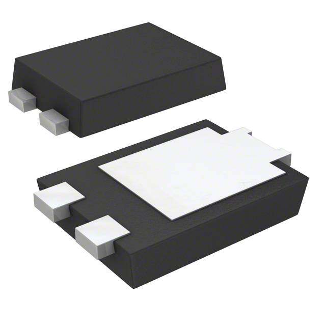
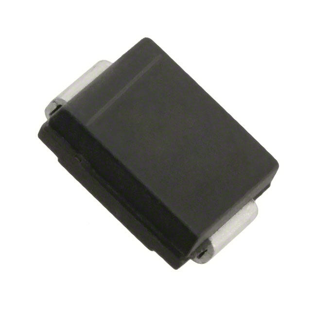
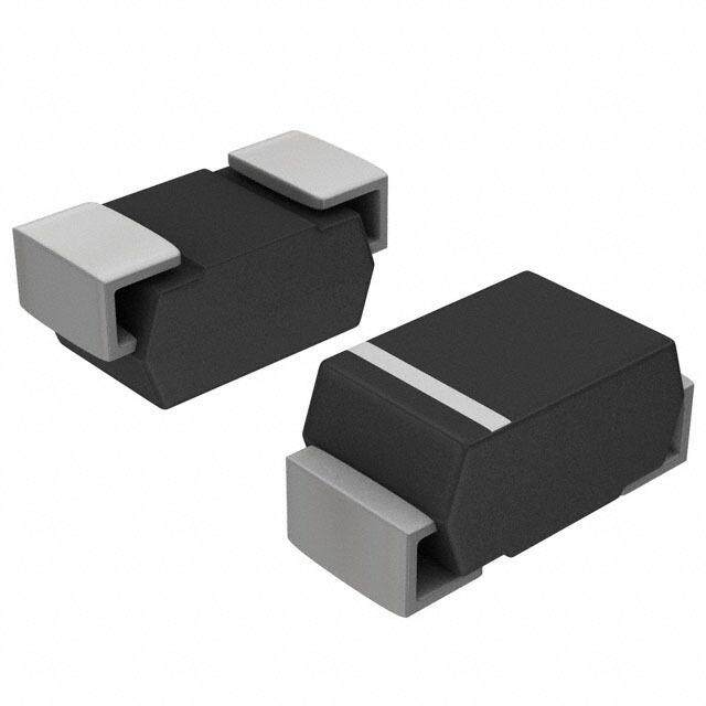
| 产品图片 |
|
| 产品型号 | SARS02 |
| rohs | 不受无铅要求限制 / 符合限制有害物质指令(RoHS)规范要求 |
| 产品系列 | - |
| 不同If时的电压-正向(Vf) | 920mV @ 1.5A |
| 不同 Vr、F时的电容 | - |
| 不同 Vr时的电流-反向漏电流 | 10µA @ 800V |
| 二极管类型 | 标准 |
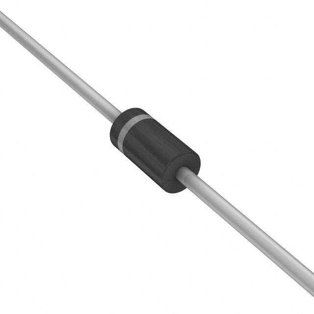
| 供应商器件封装 | 轴向 |
| 其它名称 | SARS02 DK |
| 包装 | 散装 |
| 反向恢复时间(trr) | 18µs |
| 安装类型 | 通孔 |
| 封装/外壳 | 轴向 |
| 工作温度-结 | -40°C ~ 150°C |
| 标准包装 | 100 |
| 热阻 | 15°C/W Jl |
| 电压-DC反向(Vr)(最大值) | 800V |
| 电流-平均整流(Io) | 1.2A |
| 速度 | 标准恢复 >500ns,> 200mA(Io) |


- 商务部:美国ITC正式对集成电路等产品启动337调查
- 曝三星4nm工艺存在良率问题 高通将骁龙8 Gen1或转产台积电
- 太阳诱电将投资9.5亿元在常州建新厂生产MLCC 预计2023年完工
- 英特尔发布欧洲新工厂建设计划 深化IDM 2.0 战略
- 台积电先进制程称霸业界 有大客户加持明年业绩稳了
- 达到5530亿美元!SIA预计今年全球半导体销售额将创下新高
- 英特尔拟将自动驾驶子公司Mobileye上市 估值或超500亿美元
- 三星加码芯片和SET,合并消费电子和移动部门,撤换高东真等 CEO
- 三星电子宣布重大人事变动 还合并消费电子和移动部门
- 海关总署:前11个月进口集成电路产品价值2.52万亿元 增长14.8%


PDF Datasheet 数据手册内容提取
余白上35mm Auxiliary Switch Diodes for Snubber SARS01, SARS02, SARS05, SARS10 Data Sheet Description Package The SARS(1) is an auxiliary switch diode especially SARS01 (Axial φ 2.7 / φ 0.60) designed for snubber circuits, which are used in the primary sides of flyback switched-mode power supplies. (1) (2) Being capable of reducing the ringing voltage generated at power MOSFET turn-off, the SARS02 (Axial φ 4 / φ 0.78) SARS-incorporated snubber circuits allow better cross regulation of multiple outputs. (1) (2) The SARS can also improve power supply efficiency s by partially transferring such ringing voltage into the n SARS05 (SJP 4.5 mm × 2.6 mm) secondary side of a power supply unit. g i Features s e (1) (2) ● Improves Cross Regulation D ● Reduces Noise ● Improves Efficiency w e Applications N (1) (2) (1) Cathode For switched-mode power supplies (SMPS) with (2) Anode flyback topology such as: r o ● White Goods SARS10 (TO220F-2L) f ● Adaptor ● Industrial Equipment d (1) e Typical Application d (2) n Clamp snubber e m CS RS1 (1) (2) (1) Cathode side m (2) Anode RS2 o Not to scale SARSc e R Selection Guide Controller Power Supply t R Part I VF Output Power, o AC/DC converter IC S2 Number F(AV) (max.) P * O N SARS01 1.2 A 0.92 V up to 50 W External SARS02 1.5 A 0.92 V up to 100 W Resistor SARS05 1 A 1.05 V up to 50 W Built-in 22 Ω SARS10 0.3 A 13 V up to 300 W *P represents a reference value for product selection. When O using the product, you should monitor temperature rises during actual operation. (1)The “SARS” represents any one of the SARSxx devices listed in this document. SARSxx-DSE Rev.1.2 SANKEN ELCTRIC CO., LTD. 1 Jan. 30, 2017 http://www.sanken-ele.co.jp/en © SANKEN ELECTRIC CO., LTD. 2015
SARS01, SARS02, SARS05, SARS10 Contents Description ------------------------------------------------------------------------------------------------------ 1 Contents --------------------------------------------------------------------------------------------------------- 2 Absolute Maximum Ratings --------------------------------------------------------------------------------- 3 Electrical Characteristics ------------------------------------------------------------------------------------ 4 SARS01 Rating and Characteristic Curves--------------------------------------------------------------- 5 SARS02 Rating and Characteristic Curves-------------------------------------------------------------s-- 6 n SARS05 Rating and Characteristic Curves--------------------------------------------------------------- 8 g SARS10 Rating and Characteristic Curves--------------------------------------------------i------------- 9 s Physical Dimensions and Marking Diagram -------------------------------------------e---------------- 11 D Operating Comparison of Clamp Snubber Circuit --------------------------------------------------- 13 Power Dissipation and Junction Temperature Calculation ---------------w-------------------------- 14 Parameter Setting of Snubber Circuit using SARS -------------------e-------------------------------- 15 N Reference Design of Power Supply ----------------------------------------------------------------------- 16 Important Notes ----------------------------------------------------- ----------------------------------------- 18 r o f d e d n e m m o c e R t o N SARSxx-DSE Rev.1.2 SANKEN ELCTRIC CO., LTD. 2 Jan. 30, 2017 http://www.sanken-ele.co.jp/en © SANKEN ELECTRIC CO., LTD. 2015
SARS01, SARS02, SARS05, SARS10 Absolute Maximum Ratings Unless otherwise specified, T = 25 °C, only the SARS10 incorporates a resistor (22 Ω). A Parameter Symbol Conditions Rating Unit Remarks Transient Peak Reverse Voltage V 800 V RSM Peak Repetitive Reverse Voltage V 800 V RM 1.2 SARS01 1.2 SARS02 Average Forward Current(2) I A F(AV) 1.0 SARS05 s 0.3 nSARS10 110 g SARS01 Half cycle sine i wave, positive side, 100 s SARS02 Surge Forward Current I 10 ms, 1 shot e A FSM 30 SARS05 D 1 ms, square pulse, 1.5 SARS10 1 shot w 60.5 SARS01 e N 50 SARS02 I2t Limiting Value I2t 1 ms ≤ t ≤ 10 ms A2s 4.5 SARS05 r o — SARS10 f −40 to 150 SARS01/02/05 Junction Temperature TJ d °C −20 to 125 SARS10 e d −40 to 150 SARS01/02/05 Storage Temperature T °C STG n −20 to 125 SARS10 e Power Dissipation P 3.0 W SARS10 m m o c e R t o N (2) See the derating curves of each product. SARSxx-DSE Rev.1.2 SANKEN ELCTRIC CO., LTD. 3 Jan. 30, 2017 http://www.sanken-ele.co.jp/en © SANKEN ELECTRIC CO., LTD. 2015
SARS01, SARS02, SARS05, SARS10 Electrical Characteristics Unless otherwise specified, T = 25 °C, only the SARS10 incorporates a resistor (22 Ω). A Parameter Symbol Conditions Min. Typ. Max. Unit Remarks I = 1.2 A — — 0.92 SARS01 F I = 1.5 A — — 0.92 SARS02 F Forward Voltage Drop V V F I = 1.0 A — — 1.05 SARS05 F I = 0.5 A — — 13 SARS10 F — — 10 SARS01 s — — 10 nSARS02 Reverse Leakage Current I V = V µA R R RM — — 5 g SARS05 i — — 10 s SARS10 e V = V , R RM — — 5D0 SARS01/02/05 Reverse Leakage Current under T = 100 °C H∙I J µA High Temperature R V = V , R RM — — w 100 SARS10 T = 125 °C J 2 e— 18 SARS01 N IF = IRP = 100 mA, 2 — 18 SARS02 Reverse Recovery Time trr TJ = 25 °C, µs 90% recovery point r2 — 19 SARS05 o 1 — 9 SARS10 f — — 20 SARS01 d R (3) e — — 15 °C/W SARS02 th(J-L) Thermal Resistance d — — 20 SARS05 n R (4) — — 15 °C/W SARS10 th(J-C) e m m o c e R t o N (3) R is thermal resistance between junction and lead. th(J-L) (4) R is thermal resistance between junction and case. th(J-c) SARSxx-DSE Rev.1.2 SANKEN ELCTRIC CO., LTD. 4 Jan. 30, 2017 http://www.sanken-ele.co.jp/en © SANKEN ELECTRIC CO., LTD. 2015
SARS01, SARS02, SARS05, SARS10 SARS01 Rating and Characteristic Curves 1.2 0.4 pation, P (W) F 01..80 sipation, P (W) R 0.3 Dissi 0.6 r Dis 0.2 ns er DC we w o g o 0.4 P P e i d rs 0.1 s r e a v e w e or 0.2 R D F w Sine wave 0.0 0 0 0.2 0.4 0.6 0.8 1 1.2 0 e200 400 600 800 Average Forward Current, I (A) N Reverse Voltage, V (V) F(AV) R Figure 1. IF(AV) vs. PF Power Dissipation Curves Figrure 2. VR vs. PR Power Dissipation Curves (TJ = 150 °C) o (TJ = 150 °C) f d 1.2 1.2 e d A) 1.0 n A) 1.0 Current, I (F(AV) 00..68 o m mDeC Current, I (F(AV) 00..68 Sine wDaCv e ward ec ward For 0.4 R For 0.4 Average 0.2 ot Average 0.2 N 0.0 0.0 100 110 120 130 140 150 100 110 120 130 140 150 Lead Temperature, T (°C) Lead Temperature, T (°C) L L Figure 3. T vs. I Derating Curves Figure 4. T vs. I Derating Curves L F(AV) L F(AV) (V = 0 V, T = 150 °C) (V = 800 V, T = 150 °C) R J R J SARSxx-DSE Rev.1.2 SANKEN ELCTRIC CO., LTD. 5 Jan. 30, 2017 http://www.sanken-ele.co.jp/en © SANKEN ELECTRIC CO., LTD. 2015
SARS01, SARS02, SARS05, SARS10 100 1E-03 T = 150 °C A 1E-04 10 A) (A) 1E-05 T = 100 °C ent, I(F 1 TA = 150 °C rent, I R1E-06 A rr ur u C d C 0.1 T = 25 °C se s ar A er 1E-07 n w v or T = 100 °C Re TA = 25 °C g F A 0.01 i 1E-08 s e D 0.001 1E-09 0.0 0.5 1.0 1.5 0 20 0 400 600 800 w Forward Voltage, V (V) Reverse Voltage, V (V) F e R Figure 5. V vs. I Typical Characteristics Figure N6. V vs. I Typical Characteristics F F R R r o f SARS02 Rating and Characteristic Curves d e 1.2 0.5 d n W) 1.0 m e W) 0.4 (F P (R n, P 0.8 m on, atio o pati 0.3 er Dissip 0.6 R ec wer Dissi 0.2 w 0.4 DC o o P d P t rd ar o wa 0.1 rw 0.2 N or o F F 0.0 0 Sine wave 0.0 0.2 0.4 0.6 0.8 1.0 1.2 0 200 400 600 800 Average Forward Current, IF(AV) (A) Reverse Voltage, VR (V) Figure 7. I vs. P Power Dissipation Curves Figure 8. V vs. P Power Dissipation Curves F(AV) F R R (T = 150 °C) (T = 150 °C) J J SARSxx-DSE Rev.1.2 SANKEN ELCTRIC CO., LTD. 6 Jan. 30, 2017 http://www.sanken-ele.co.jp/en © SANKEN ELECTRIC CO., LTD. 2015
SARS01, SARS02, SARS05, SARS10 1.2 1.2 A) 1.0 A) 1.0 (V) (V) Sine wave A A nt, IF( 0.8 DC nt, IF( 0.8 urre 0.6 urre 0.6 DC C C d d war war s or 0.4 or 0.4 n F F e e g g g era 0.2 era 0.2 si v v A A e D 0.0 0.0 100 110 120 130 140 150 100 110 120 130 140 150 w Lead Temperature, T (°C) Lead Temperature, T (°C) L e L N Figure 9. T vs. I Derating Curves Figure 10. T vs. I Derating Curves L F(AV) L F(AV) (V = 0 V, T = 150 °C) (V = 800 V, T = 150 °C) R J r R J o f 100 1E-03 d T = 150 °C e A d 1E-04 10 n A) e A) 1E-05 (F m (R urrent, I 1 TA = 150 °C m urrent, I 1E-06 TA = 100 °C d C 0.1 o TA = 25 °C e C r c s wa er 1E-07 TA = 25 °C For R e TA = 100 °C Rev 0.01 1E-08 t o N 0.001 1E-09 0.0 0.5 1.0 1.5 0 200 400 600 800 Forward Voltage, V (V) Reverse Voltage, V (V) F R Figure 11. V vs. I Typical Characteristics Figure 12. V vs. I Typical Characteristics F F R R SARSxx-DSE Rev.1.2 SANKEN ELCTRIC CO., LTD. 7 Jan. 30, 2017 http://www.sanken-ele.co.jp/en © SANKEN ELECTRIC CO., LTD. 2015
SARS01, SARS02, SARS05, SARS10 SARS05 Rating and Characteristic Curves 1.4 0.4 1.2 ) W) (W P (F 1.0 n, P R 0.3 pation, 0.8 sipatio ssi Dis 0.2 s r Di 0.6 wer n Powe 0.4 d Po ig orward 0.2 DC Forwar 0.1 D es F w Sine wave 0.0 0 0.0 0.2 0.4 0.6 0.8 1.0 0 e200 400 600 800 Average Forward Current, I (A) N Reverse Voltage, V (V) F(AV) R r Figure 13. I vs. P Power Dissipation Curves Figure 14. V vs. P Power Dissipation Curves F(AV) F R R o (T = 150 °C) (T = 150 °C) J J f d 1.0 e 1.0 d 0.9 0.9 I (A) F(AV) 00..78 m e D Cn (A) F(AV) 00..78 rent, 0.6 m ent, I 0.6 Cur 0.5 o Curr 0.5 Sine wave ward 0.4 ec ard 0.4 DC w or R r F 0.3 o ge e F 0.3 vera 0.2 ot erag 0.2 A v 0.1 N A 0.1 0.0 0.0 100 110 120 130 140 150 100 110 120 130 140 150 Lead Temperature, T ( °C) Lead Temperature, T (°C) L L Figure 15. T vs. I Derating Curves Figure 16. T vs. I Derating Curves L F(AV) L F(AV) (V = 0 V, T = 150 °C) (V = 800 V, T = 150 °C) R J R J SARSxx-DSE Rev.1.2 SANKEN ELCTRIC CO., LTD. 8 Jan. 30, 2017 http://www.sanken-ele.co.jp/en © SANKEN ELECTRIC CO., LTD. 2015
SARS01, SARS02, SARS05, SARS10 100 1E-04 T = 150 °C A 1E-05 10 nt, I(A) F 1 TA = 150 °C nt, I (A) R1E-06 TA = 100 °C urre TA = 25 °C urre 1E-07 C C ward 0.1 TA = 100 °C verse 1E-08 TA = 25 °C ns or Re g F 0.01 i 1E-09 s e D 0.001 1E-10 0.0 0.5 1.0 1.5 0 20 0 400 600 800 w Forward Voltage, V (V) Reverse Voltage, V (V) F e R N Figure 17. V vs. I Typical Characteristics Figure 18. V vs. I Typical Characteristics F F R R r o f SARS10 Rating and Characteristic Curves d e 3.0 d 0.08 n 0.07 ) e (W m W) P F (R 0.06 wer Dissipation, 2.0 R eco m DC er Dissipation, P 000...000345 o w P 1.0 o ward ot ard P 0.02 or N rw F o F 0.01 0.0 0 0.0 0.1 0.2 0.3 0 100 200 300 400 500 600 700 800 Average Forward Current, I (A) Reverse Voltage, V (V) F(AV) R Figure 19. I vs. P Power Dissipation Curves Figure 20. V vs. P Power Dissipation Curve F(AV) F R R (T = 125 °C) (T = 125 °C) J J SARSxx-DSE Rev.1.2 SANKEN ELCTRIC CO., LTD. 9 Jan. 30, 2017 http://www.sanken-ele.co.jp/en © SANKEN ELECTRIC CO., LTD. 2015
SARS01, SARS02, SARS05, SARS10 0.3 1 DC A) (V) urrent, IF(A 0.2 ent, I(A) F 0.1 C rr d Cu r wa d s r or 0.1 wa 0.01 n F r rage Fo TA = 150 °C ig ve T = 100 °C s A A e TA = 25 D°C 0.001 0.0 0 5 10 15 20 50 60 70 80 90 100 110 120 130 w Forward Voltage, V (V) Case Temperature, T (°C) F C e N Figure 21. T vs. I Derating Curves Figure 22. V vs. I Typical Characteristics C F(AV) F F (V = 800 V, T = 125 °C) R J r o f 1E-04 d e T = 150 °C 1E-05 A d n ) A e (R 1E-06 m I nt, e T = 100 °C m rr 1E-07 A u C e o s ver 1E-08 TA = 25 °C c e e R R 1E-09 t o N 1E-10 0 200 400 600 800 Reverse Voltage, V (V) R Figure 23. V vs. I Typical Characteristics R R SARSxx-DSE Rev.1.2 SANKEN ELCTRIC CO., LTD. 10 Jan. 30, 2017 http://www.sanken-ele.co.jp/en © SANKEN ELECTRIC CO., LTD. 2015
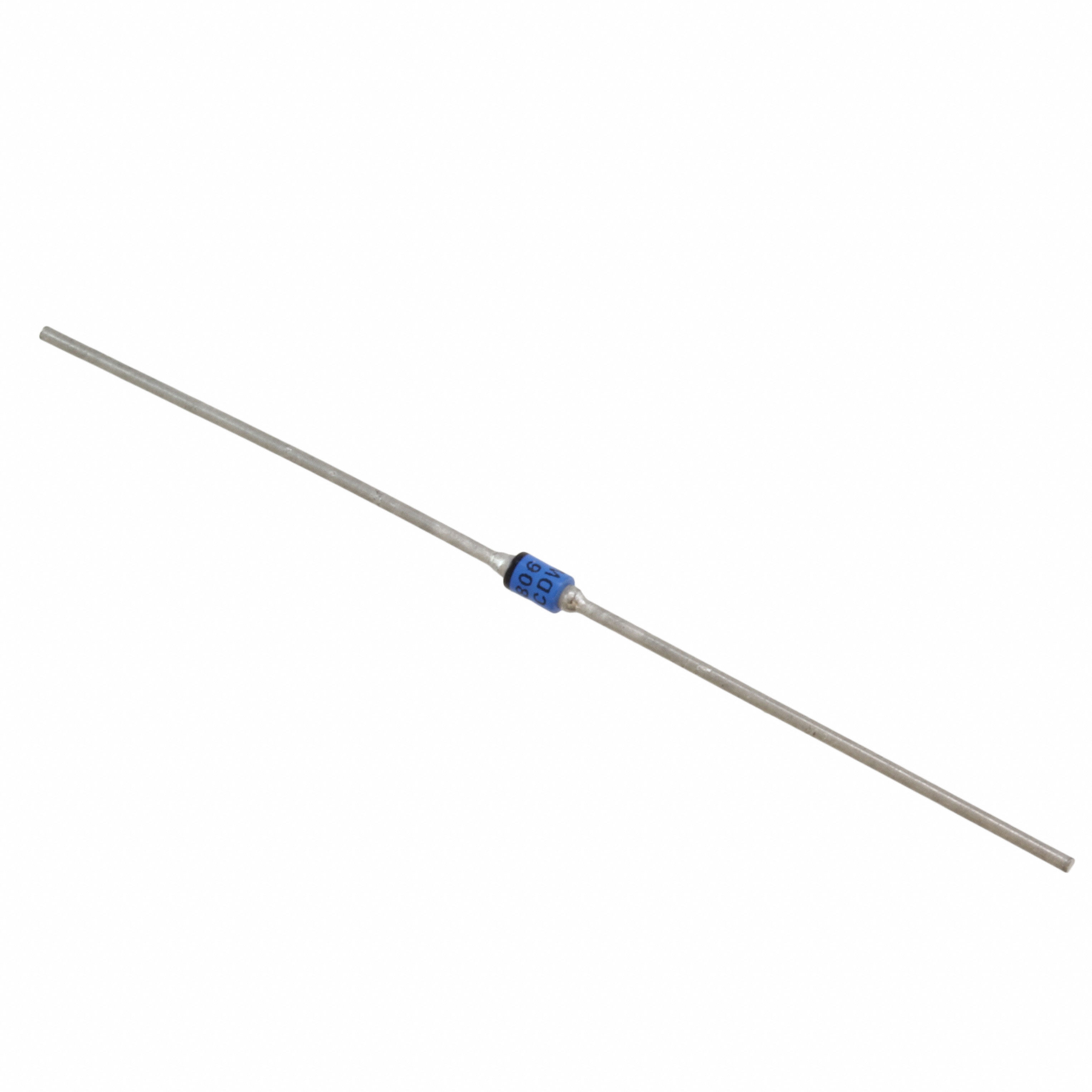
SARS01, SARS02, SARS05, SARS10 Physical Dimensions and Marking Diagrams ● SARS01 Axial (φ 2.7 / φ 0.6) Polarity Marking (Cathode band) Device Code of SARS01 AR S1 Y M D s n Lot Number: g Y is the last digit of the year of manufacture (0 to 9) i M is the month of the year (1 to 9, O, Ns, or D) D is a period of days: e “・” is the first 10 days of the mDonth (1st to 10th) “・・” is the second 10 days of the month (11th to 20th) “・・・” is the last 10–11w days of the month (21st to 31st) NOTES: e - Dimensions in millimeters N - Bare lead: Pb-free (RoHS compliant) - When soldering the products, be sure to minimize the working time, within the following limits: Flow: 260 ± 5 °C / 10 ± 1 s, 2 times r Soldering Iron: 380 ± 10 °C / 3.5 ± 0.5 s, 1 time (Soldering sohould be at a distance of at least 1.5 mm from the body of the products.) f d e ● SARS02 d Axial (φ 4 / φ 0.78) n e Polarity Marking (Cathode band) m SARS2 SARS2 Device Code of SARS02 m Y M D Y M D o c e Lot Number: Y is the last digit of the year of manufacture (0 to 9) R M is the month of the year (1 to 9, O, N, or D) D is a period of days: t “・” is the first 10 days of the month (1st to 10th) o “・・” is the second 10 days of the month (11th to 20th) N “・・・” is the last 10–11 days of the month (21st to 31st) NOTES: - Dimensions in millimeters - Bare lead: Pb-free (RoHS compliant) - When soldering the products, be sure to minimize the working time within the following limits: Flow: 260 ± 5 °C / 10 ± 1 s, 2 times Soldering iron: 380 ± 10 °C / 3.5 ± 0.5 s, 1 time (Soldering should be at a distance of at least 1.5 mm from the body of the products.) SARSxx-DSE Rev.1.2 SANKEN ELCTRIC CO., LTD. 11 Jan. 30, 2017 http://www.sanken-ele.co.jp/en © SANKEN ELECTRIC CO., LTD. 2015
SARS01, SARS02, SARS05, SARS10 ● SARS05 SJP 4.5 mm × 2.6 mm AS05 Device Code of SARS05 Y M D D Lot Number: Y is the last digit of the year of manufacture (0 to 9) M is the month of the year (1 to 9, O, N, or D) DD is the day of the month (01 to 31) s n Polarity Marking (Cathode band) g i NOTES: s SJP Land Pattern Example - Dimensions in millimeters e - Bare lead frame: Pb-free (RoHDS compliant) 2.0 - When soldering the products, be sure to minimize the working time, within the following limits: w Reflow (MSL 1): Preheat: 180 °Ce, 90 ± 30 s Solder heatinNg: 250 °C, 10 ± 1s, 2 times (260 °C peak) 2.0 Soldering iron: 380 ± 10 °C, 3.5 ± 0.5s, 1 time 4.0 to 4.2 r o f ● SARS10 d TO220F-2L e d n e m m o c SARS10 e Part Number R Y M D D Lot Number: t Y is the last digit of the year of manufacture (0 to 9) o M is the month of the year (1 to 9, O, N, or D) N DD is the day of the month (01 to 31) 1 2 NOTES: - Dimensions in millimeters - Bare lead frame: Pb-free (RoHS compliant) - When soldering the products,be sure to minimize the working time, within the following limits: Flow: 260 ± 5 °C / 10 ± 1 s, 2 times Soldering Iron: 380 ± 10 °C / 3.5 ± 0.5 s, 1 time (Soldering should be at a distance of at least 1.5 mm from the body of the products.) - The recommended screw torque for TO220F: 0.490 N∙m to 0.686 N∙m (5 kgf∙cm to 7 kgf∙cm) SARSxx-DSE Rev.1.2 SANKEN ELCTRIC CO., LTD. 12 Jan. 30, 2017 http://www.sanken-ele.co.jp/en © SANKEN ELECTRIC CO., LTD. 2015
SARS01, SARS02, SARS05, SARS10 Operational Comparison of Clamp Snubber Figure 27 shows the clamp snubber circuit using the Circuits SARS. The surge voltage at tuning off a power MOSFET is charged to C through the surge absorb loop. S Figure 24 shows a general clamp snubber circuit. In Since the reverse recovery time, trr, of the SARS is a the circuit, the surge voltage at tuning off a power relatively long period, the energy charged to C is S MOSFET is charged to C through the surge absorb loop, discharged to the reverse direction of the surge absorb S and is consumed by R through the energy discharge loop until C voltage is equal to the flyback voltage. S1 S loop. All the consumed energy becomes loss in R . In Some discharged energy is transferred to secondary side. S1 addition, the ringing of surge voltage results in poor Thus, the power supply efficiency improves. cross regulation of multi-outputs. In addition, the power supply using the SARS reduces the ringing voltage. Thus, the cross regulation of multi-outputs can be improved. s n Egnergy RS1 CS idischarge loop s Edinsechrgayrg e looDpFRD RS1 DCS e RS2 ID Surge absorb loop wSARS Controller VDS e ID Surge absorb loop N AC/DC converter IC Controller VDS Figure 24. General Clamp Snubber Circuit r AC/DC converter IC o fFigure 27. Clamp Snubber Circuit using SARS R : 570 kΩ d S1 CS: 1000 pF e DFRD: EG01C d RS1: 570 kΩ VDS ID n RCS2: :1 2020 0Ω p F S e V SARS: SARS01 DS I m D m o c Figure 25. Waveforms oef General Clamp Snubber CRircuit Figure 28. Waveforms of Clamp Snubber Circuit using t SARS o N ID VDS ID VDS Figure 26. Enlarged View of Figure 25 Figure 29. Enlarged View of Figure 28 SARSxx-DSE Rev.1.2 SANKEN ELCTRIC CO., LTD. 13 Jan. 30, 2017 http://www.sanken-ele.co.jp/en © SANKEN ELECTRIC CO., LTD. 2015
SARS01, SARS02, SARS05, SARS10 Power Dissipation and Junction t t t … t 1 2 3 k Temperature Calculation ISARS Figure 30 shows a typical application using the SARS. 0 Figure 31 shows the operating waveforms of the SARS. The power dissipation of the SARS is calculated as V follows: SARS 0 1) The waveforms of the SARS voltage, V , and the SARS SARS current, I , are measured in actual SARS application operation. V × I is calculated by SARS SARS Energy P1 P2 P3 … Pk the math function of oscilloscope. (Since the SARS10 incorporates a resistor, V 0 s SARS(10) is measured.) T n 2) The each average energy (P , P …P ) is measured at g 1 2 k period of each polarity of V × I (t , t ,…t ) as i SARS SARS 1 2 k s shown in Figure 30 by the automatic measurement Figure 31. SAeRS Current function of the oscilloscope. D 3) The power dissipation of the SARS, P , is SARS calucultaed by Equation (1): In addition, by usin g the temperature of the SARS in w actual application operation, the estimated junction temperature of tehe SARS is calculated by Equation (2) (1) and EquationN (3). It should be enough lower than TJ of the absolute maximum rating. r where: ● SARS01/02/05 o P is power dissipation of the SARS, SARS f T is switching cycle of power MOSFET (s), and (2) P is average energy of period t (W). d k k e where: A differential probe is recommended to use for tdhe T is junction temperature of the SARS, measurement of V . Please conform to the J(SARS) SARS n T is lead temperature of the SARS, and oscilloscope manual about power dissipation L measurement including the delay compenseation of J-L is thermal resistance between junction to lead. m probe. ● SARS10 m (3) o R C S1 S c Where: e RS2 R TJ(SARS) is junction temperature of the SARS, T is case temperature of the SARS, and V C SARS(10) VSARS ISARS J-C is thermal resistance between junction to case. t SARS o N Controller AC/DC converter IC Figure 30. Typical Application SARSxx-DSE Rev.1.2 SANKEN ELCTRIC CO., LTD. 14 Jan. 30, 2017 http://www.sanken-ele.co.jp/en © SANKEN ELECTRIC CO., LTD. 2015
SARS01, SARS02, SARS05, SARS10 Parameter Setting of Snubber Circuit using SARS The temperature of the SARS and peripheral components should be measured in actual application operation. The reference values of snubber circuit using the SARS are as follows: ● C S 680 pF to 0.01 μF. The voltage rating is selected according to the voltage s subtraced the input voltage from the peak of VDS. n g ● R S1 i RS1 is the bias resistance to turn off the SARS, and is s 100 kΩ to 1 MΩ. e Since a high voltage is applied to R that has high D S1 resistance, the following should be considered according to the requirement of the application: w - Select a resistor designed for electromigration, or - Connect more resistors in series so that the applied e N voltages of individual resistors can be reduced. The power rating of resistor should be selected from the measurement of the effective current of R based on r S1 actual operation in the application. o f ● RS2 d R is the limited resistance in the energy discharging. S2 e The value of 22 Ω to 220 Ω is connected to the SARS in d series (the SARS10 incorporates R ). S2 n The power rating of resistor should be selected from the measurement of the effective current of R e based on S2 actual operation in the application. m m o c e R t o N SARSxx-DSE Rev.1.2 SANKEN ELCTRIC CO., LTD. 15 Jan. 30, 2017 http://www.sanken-ele.co.jp/en © SANKEN ELECTRIC CO., LTD. 2015
SARS01, SARS02, SARS05, SARS10 Reference Design of Power Supply This section provides the information on a reference design, including power supply specifications, a circuit diagram, the bill of materials, and transformer specifications. ● Power Supply Specifications Item Specification Input Voltage 85 VAC to 265 VAC Output Power 34.8 W (40.4 W peak) Output 1 8 V / 0.5 A Output 2 14 V / 2.2 A (2.6 A peak) s n ● Circuit Schematic g 1 F1 i L1 s D1 D2 T1 D51 e VOUT1 C1 (+) D4 D3 D C3 R1 S1 3 C2 C51 C52 w R2 (-) D52 e D5 P1 OUT2 N (+) U1 R51 R54 5 D/ST FB/OLP 4 S2 r Co53 R55 6 DNC/ST GND 3 R52 D6 R3 f PC1 7 D/ST VCC 2 d R53 C54 D/ST S/OCP C5 D 8 1 e U51 STR3A400 d R56 C6 R4 C4 PC1 n (-) C7 e m ● Bill of Materials Symbol Ratings(1) Rmecommended Part No. Symbol Ratings(1) Recommended Part No. C1(2) Film, 0.1 μF, 275 V D52 Schottky, 100 V, 10 A FMEN-210A C2(2) Electrolytic, 150 μF, 400 Vo F1 Fuse, 250 V AC, 3 A C3 Ceramic, 1000 pF, 1 kVc L1(2) CM inductor, 3.3 mH C4 Ceramic, 0.01 μF e PC1 Optocoupler, PC123 or equiv. C5 Electrolytic, 22 μRF, 50 V R1(3) Metal oxide, 330 kΩ, 1 W C6(2) Ceramic, 15 pF / 2 kV R2 47 Ω, 1 W C7(2) Ceramic, 2t200 pF, 250 V R3 10 Ω C51(2) Electroloytic, 680 μF, 25 V R4(2) 0.47 Ω, 1/2 W N C52 Electrolytic, 680 μF, 25 V R51 1 kΩ C53 Electrolytic, 470 μF, 16 V R52 1.5 kΩ C54(2) Ceramic, 0.1 μF, 50 V R53(2) 100 kΩ D1 600 V, 1 A EM01A R54(2) 6.8 kΩ D2 600 V, 1 A EM01A R55 ± 1%, 39 kΩ D3 600 V, 1 A EM01A R56 ± 1%, 10 kΩ See the Transformer D4 600 V, 1 A EM01A T1 Specification D5 800 V, 1.2 A SARS01 U1 IC, STR3A453D D6 Fast recovery, 200 V, 1 A AL01Z U51 Shunt regulator, V = 2.5 V (TL431 or equiv.) REF D51 Schottky, 60 V, 1.5 A EK16 (1) Unless otherwise specified, the voltage rating of capacitor is 50 V or less and the power rating of resistor is 1/8 W or less. (2) Refers to a part that requires adjustment based on operation performance in an actual application. (3) High voltage is applied to this resistor that has high resistance. To meet your application requirements, it is required to select resistors designed for electromigration, or to connect more resistors in series so that the applied voltages of individual resistors can be reduced. SARSxx-DSE Rev.1.2 SANKEN ELCTRIC CO., LTD. 16 Jan. 30, 2017 http://www.sanken-ele.co.jp/en © SANKEN ELECTRIC CO., LTD. 2015
SARS01, SARS02, SARS05, SARS10 ● Transformer Specifications Item Specification Primary Inductance, L 518 μH P Core Size EER-28 AL Value 245 nH/N2 (with a center gap of about 0.56 mm) Winding Specification See Table 1 Winding Structure See Figure 32 Table 1. Winding Specification s n Number of Turns Winding Symbol Wire Diameter (mm) Sgtructure (turns) i Primary Winding P1 18 φ 0.23 × 2 Single-lsayer, solenoid winding e Primary Winding P2 28 φ 0.30 Single-layer, solenoid winding D Auxiliary Winding D 12 φ 0.30 × 2 Solenoid winding Output 1 Winding S1-1 6 φ 0.4 × 2 Solenoid winding w Output 1 Winding S1-2 6 φ 0.4 × 2 Solenoid winding e Output 2 Winding S2-1 4 φ 0.4 × 2 Solenoid winding N Output 2 Winding S2-2 4 φ 0.4 × 2 Solenoid winding r o f d 2 mm 4 mm e d VDC n P2 8 V P1 e Margin tape SS22--12DSS11--12 Margin tapem n sidem Drain P1 S1-1 S1-2 14 V Pi P2 VCC o S2-1 S2-2 Bobbin D c GND eCore GND R ● denotes the start of winding. Cross-section View t o Figure 32. Winding Structure N SARSxx-DSE Rev.1.2 SANKEN ELCTRIC CO., LTD. 17 Jan. 30, 2017 http://www.sanken-ele.co.jp/en © SANKEN ELECTRIC CO., LTD. 2015
SARS01, SARS02, SARS05, SARS10 Important Notes ● All data, illustrations, graphs, tables and any other information included in this document as to Sanken’s products listed herein (the “Sanken Products”) are current as of the date this document is issued. All contents in this document are subject to any change without notice due to improvement of the Sanken Products, etc. Please make sure to confirm with a Sanken sales representative that the contents set forth in this document reflect the latest revisions before use. ● The Sanken Products are intended for use as components of general purpose electronic equipment or apparatus (such as home appliances, office equipment, telecommunication equipment, measuring equipment, etc.). Prior to use of the Sanken Products, please put your signature, or affix your name and seal, on the specification documents of the Sanken Products and return them to Sanken. When considering use of the Sanken Products for any applications that require higher reliability (such as transportation equipment and its control systems, traffic signal control systems or equipment, disaster/crime alarm systems, various safety devices, etc.), you must contact a Sanken sales representative to discuss the suitability of such use and put your signature, or affix your name and seal, on the specification documents of the Sanken Products and return them to Sanken, prior to the use of the s Sanken Products. The Sanken Products are not intended for use in any applications that require extremely high reliability such as: n aerospace equipment; nuclear power control systems; and medical equipment or systems, whose failure or malfunction may result in death or serious injury to people, i.e., medical devices in Class III or a higher class as defined by reglevant laws of Japan (collectively, the “Specific Applications”). Sanken assumes no liability or responsibility whatsoever for iany and all damages and losses that may be suffered by you, users or any third party, resulting from the use of the Sankens Products in the Specific Applications or in manner not in compliance with the instructions set forth herein. e ● In the event of using the Sanken Products by either (i) combining other products or materiDals therewith or (ii) physically, chemically or otherwise processing or treating the same, you must duly consider all possible risks that may result from all such uses in advance and proceed therewith at your own responsibility. w ● Although Sanken is making efforts to enhance the quality and reliability of its products, it is impossible to completely avoid the occurrence of any failure or defect in semiconductor products at a certain rate. Yeou must take, at your own responsibility, preventative measures including using a sufficient safety design and confirming sNafety of any equipment or systems in/for which the Sanken Products are used, upon due consideration of a failure occurrence rate or derating, etc., in order not to cause any human injury or death, fire accident or social harm which may result from any failure or malfunction of the Sanken Products. Please refer r to the relevant specification documents and Sanken’s official website in relation to derating. ● No anti-radioactive ray design has been adopted for the Sanken Products.o ● No contents in this document can be transcribed or copied without Safnken’s prior written consent. ● The circuit constant, operation examples, circuit examples, pattern layout examples, design examples, recommended examples, all d information and evaluation results based thereon, etc., described in this document are presented for the sole purpose of reference of use of the Sanken Products and Sanken assumes no responesibility whatsoever for any and all damages and losses that may be suffered by you, users or any third party, or any possible idnfringement of any and all property rights including intellectual property rights and any other rights of you, users or any third panrty, resulting from the foregoing. ● All technical information described in this document (the “Technical Information”) is presented for the sole purpose of reference e of use of the Sanken Products and no license, express, implied or otherwise, is granted hereby under any intellectual property rights or any other rights of Sanken. m ● Unless otherwise agreed in writing between Sanken and you, Sanken makes no warranty of any kind, whether express or implied, including, without limitation, any warranmty (i) as to the quality or performance of the Sanken Products (such as implied warranty of merchantability, or implied warranty of fitness for a particular purpose or special environment), (ii) that any Sanken Product is delivered free of claims of third paroties by way of infringement or the like, (iii) that may arise from course of performance, course of dealing or usage of trade, ancd (iv) as to any information contained in this document (including its accuracy, usefulness, or reliability). e ● In the event of using the SRanken Products, you must use the same after carefully examining all applicable environmental laws and regulations that regulate the inclusion or use of any particular controlled substances, including, but not limited to, the EU RoHS Directive, so as to be in strict compliance with such applicable laws and regulations. t ● You must not use the Sanken Products or the Technical Information for the purpose of any military applications or use, including o but not limited to the development of weapons of mass destruction. In the event of exporting the Sanken Products or the Technical N Information, or providing them for non-residents, you must comply with all applicable export control laws and regulations in each country including the U.S. Export Administration Regulations (EAR) and the Foreign Exchange and Foreign Trade Act of Japan, and follow the procedures required by such applicable laws and regulations. ● Sanken assumes no responsibility for any troubles, which may occur during the transportation of the Sanken Products including the falling thereof, out of Sanken’s distribution network. ● Although Sanken has prepared this document with its due care to pursue the accuracy thereof, Sanken does not warrant that it is error free and Sanken assumes no liability whatsoever for any and all damages and losses which may be suffered by you resulting from any possible errors or omissions in connection with the contents included herein. ● Please refer to the relevant specification documents in relation to particular precautions when using the Sanken Products, and refer to our official website in relation to general instructions and directions for using the Sanken Products. ● All rights and title in and to any specific trademark or tradename belong to Sanken or such original right holder(s). DSGN-CEZ-16002 SARSxx-DSE Rev.1.2 SANKEN ELCTRIC CO., LTD. 18 Jan. 30, 2017 http://www.sanken-ele.co.jp/en © SANKEN ELECTRIC CO., LTD. 2015