ICGOO在线商城 > 集成电路(IC) > 时钟/计时 - 可编程计时器和振荡器 > SA555P
 Datasheet下载
- 型号: SA555P
- 制造商: Texas Instruments
- 库位|库存: xxxx|xxxx
- 要求:
| 数量阶梯 | 香港交货 | 国内含税 |
| +xxxx | $xxxx | ¥xxxx |
查看当月历史价格
查看今年历史价格
SA555P产品简介:
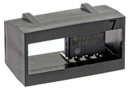
ICGOO电子元器件商城为您提供SA555P由Texas Instruments设计生产,在icgoo商城现货销售,并且可以通过原厂、代理商等渠道进行代购。 SA555P价格参考¥0.57-¥1.63。Texas InstrumentsSA555P封装/规格:时钟/计时 - 可编程计时器和振荡器, 555 Type, Timer/Oscillator (Single) IC 100kHz 8-PDIP。您可以下载SA555P参考资料、Datasheet数据手册功能说明书,资料中有SA555P 详细功能的应用电路图电压和使用方法及教程。
SA555P是Texas Instruments(德州仪器)生产的经典555定时器芯片的一种型号,属于可编程计时器和振荡器类别。它是一种多功能的集成电路,广泛应用于各种电子电路中,主要用于生成精确的时间延迟或振荡信号。以下是SA555P的主要应用场景:

1. 定时器应用
   - 单稳态模式:在接收到触发信号后,输出一个固定时间长度的脉冲。这种模式常用于延时开关、定时控制等场景,例如家用电器的自动关闭功能。
   - 多稳态模式:产生连续的方波信号,适用于音频信号发生器、PWM(脉宽调制)控制器等。

2. 脉冲宽度调制(PWM)
   - SA555P可以用来生成不同占空比的方波信号,用于控制电机速度、LED亮度调节或直流-直流转换器中的开关电源控制。

3. 振荡器
   - 在自由运行的多谐振荡器模式下,SA555P可以产生稳定的频率信号,适用于时钟信号生成、蜂鸣器驱动、无线发射器调制等。

4. 电子玩具和乐器
   - 由于其能够生成音频范围内的频率信号,SA555P常被用于简单的电子音乐合成器、音效发生器或儿童玩具中的声音模块。

5. 传感器信号处理
   - 可用于设计基于红外、超声波或其他传感器的检测系统,通过定时器功能实现信号的周期性发送与接收。

6. 电源管理
   - 在低功耗设备中,SA555P可用于间歇性地激活某些电路组件,以减少整体能耗。

7. 工业控制
   - 用于工厂自动化中的定时任务,例如流水线上的物料输送控制、周期性检测设备的启动与停止。

8. 教育与实验
   - 因其结构简单、易于理解,SA555P也广泛应用于电子学教学和学生实验中,帮助初学者学习基本的模拟和数字电路知识。

总之,SA555P凭借其可靠性、灵活性和低成本,在消费电子、工业控制、通信设备以及教育领域都有广泛应用。
| 参数 | 数值 |
| 产品目录 | 集成电路 (IC)半导体 |
| 描述 | IC OSC SINGLE TIMER 100KHZ 8-DIP计时器和支持产品 Precision |
| 产品分类 | |
| 品牌 | Texas Instruments |
| 产品手册 | |
| 产品图片 |
|
| rohs | 符合RoHS无铅 / 符合限制有害物质指令(RoHS)规范要求 |
| 产品系列 | 时钟和计时器IC,计时器和支持产品,Texas Instruments SA555P- |
| 数据手册 | |
| 产品型号 | SA555P |
| 产品目录页面 | |
| 产品种类 | 计时器和支持产品 |
| 供应商器件封装 | 8-PDIP |
| 其它名称 | 296-9682-5 |
| 内部定时器数量 | 1 |
| 包装 | 管件 |
| 单位重量 | 440.400 mg |
| 商标 | Texas Instruments |
| 安装类型 | 通孔 |
| 安装风格 | Through Hole |
| 封装 | Tube |
| 封装/外壳 | 8-DIP(0.300",7.62mm) |
| 封装/箱体 | PDIP-8 |
| 工作温度 | -40°C ~ 85°C |
| 工厂包装数量 | 50 |
| 最大工作温度 | + 85 C |
| 最小工作温度 | - 40 C |
| 标准包装 | 50 |
| 电压-电源 | 4.5 V ~ 16 V |
| 电流-电源 | 10mA |
| 电源电压-最大 | 16 V |
| 电源电压-最小 | 4.5 V |
| 电源电流 | 2000 uA |
| 类型 | 555 型,计时器/振荡器(单路) |
| 系列 | SA555 |
| 计数 | - |
| 频率 | 100kHz |


- 商务部:美国ITC正式对集成电路等产品启动337调查
- 曝三星4nm工艺存在良率问题 高通将骁龙8 Gen1或转产台积电
- 太阳诱电将投资9.5亿元在常州建新厂生产MLCC 预计2023年完工
- 英特尔发布欧洲新工厂建设计划 深化IDM 2.0 战略
- 台积电先进制程称霸业界 有大客户加持明年业绩稳了
- 达到5530亿美元!SIA预计今年全球半导体销售额将创下新高
- 英特尔拟将自动驾驶子公司Mobileye上市 估值或超500亿美元
- 三星加码芯片和SET,合并消费电子和移动部门,撤换高东真等 CEO
- 三星电子宣布重大人事变动 还合并消费电子和移动部门
- 海关总署:前11个月进口集成电路产品价值2.52万亿元 增长14.8%


PDF Datasheet 数据手册内容提取
Product Sample & Technical Tools & Support & Folder Buy Documents Software Community NA555,NE555,SA555,SE555 SLFS022I–SEPTEMBER1973–REVISEDSEPTEMBER2014 xx555 Precision Timers 1 Features 3 Description • TimingFromMicrosecondstoHours These devices are precision timing circuits capable of 1 producing accurate time delays or oscillation. In the • AstableorMonostableOperation time-delay or mono-stable mode of operation, the • AdjustableDutyCycle timed interval is controlled by a single external • TTL-CompatibleOutputCanSinkorSource resistor and capacitor network. In the a-stable mode Upto200mA of operation, the frequency and duty cycle can be controlled independently with two external resistors • OnProductsComplianttoMIL-PRF-38535, andasingleexternalcapacitor. AllParametersAreTestedUnlessOtherwise Noted.OnAllOtherProducts,Production The threshold and trigger levels normally are two- ProcessingDoesNotNecessarilyInclude thirds and one-third, respectively, of VCC. These levels can be altered by use of the control-voltage TestingofAllParameters. terminal. When the trigger input falls below the trigger level, the flip-flop is set, and the output goes high. If 2 Applications the trigger input is above the trigger level and the • FingerprintBiometrics threshold input is above the threshold level, the flip- flop is reset and the output is low. The reset (RESET) • IrisBiometrics input can override all other inputs and can be used to • RFIDReader initiate a new timing cycle. When RESET goes low, the flip-flop is reset, and the output goes low. When the output is low, a low-impedance path is provided betweendischarge(DISCH)andground. The output circuit is capable of sinking or sourcing current up to 200 mA. Operation is specified for supplies of 5 V to 15 V. With a 5-V supply, output levelsarecompatiblewithTTLinputs. DeviceInformation(1) PARTNUMBER PACKAGE BODYSIZE(NOM) PDIP(8) 9.81mm×6.35mm SOP(8) 6.20mm×5.30mm xx555 TSSOP(8) 3.00mm×4.40mm SOIC(8) 4.90mm×3.91mm (1) For all available packages, see the orderable addendum at theendofthedatasheet. 4 Simplified Schematic VCC RESET 8 CONT 4 5 Î Î 6 R1 THRES Î Î Î Î 3 Î R 1Î Î OUT Î Î Î S Î Î 2 TRIG Î Î 7 DISCH 1 GND 1 An IMPORTANT NOTICE at the end of this data sheet addresses availability, warranty, changes, use in safety-critical applications, intellectualpropertymattersandotherimportantdisclaimers.PRODUCTIONDATA.
NA555,NE555,SA555,SE555 SLFS022I–SEPTEMBER1973–REVISEDSEPTEMBER2014 www.ti.com Table of Contents 1 Features.................................................................. 1 8.1 Overview...................................................................9 2 Applications........................................................... 1 8.2 FunctionalBlockDiagram.........................................9 3 Description............................................................. 1 8.3 FeatureDescription...................................................9 8.4 DeviceFunctionalModes........................................12 4 SimplifiedSchematic............................................. 1 9 ApplicationsandImplementation...................... 13 5 RevisionHistory..................................................... 2 9.1 ApplicationInformation............................................13 6 PinConfigurationandFunctions......................... 3 9.2 TypicalApplications................................................13 7 Specifications......................................................... 4 10 PowerSupplyRecommendations..................... 18 7.1 AbsoluteMaximumRatings .....................................4 11 DeviceandDocumentationSupport................. 19 7.2 HandlingRatings.......................................................4 11.1 RelatedLinks........................................................19 7.3 RecommendedOperatingConditions.......................4 11.2 Trademarks...........................................................19 7.4 ElectricalCharacteristics...........................................5 11.3 ElectrostaticDischargeCaution............................19 7.5 OperatingCharacteristics..........................................6 11.4 Glossary................................................................19 7.6 TypicalCharacteristics..............................................7 12 Mechanical,Packaging,andOrderable 8 DetailedDescription.............................................. 9 Information........................................................... 19 5 Revision History ChangesfromRevisionH(June2010)toRevisionI Page • UpdateddocumenttonewTIenhanceddatasheetformat................................................................................................... 1 • DeletedOrderingInformationtable. ...................................................................................................................................... 1 • AddedMilitaryDisclaimertoFeatureslist.............................................................................................................................. 1 • AddedApplications................................................................................................................................................................. 1 • AddedDeviceInformationtable............................................................................................................................................. 1 • MovedT toHandlingRatingstable..................................................................................................................................... 4 stg • AddedDISCHswitchon-statevoltageparameter.................................................................................................................. 5 • AddedDeviceandDocumentationSupportsection............................................................................................................. 19 • AddedESDwarning............................................................................................................................................................. 19 • AddedMechanical,Packaging,andOrderableInformationsection..................................................................................... 19 2 SubmitDocumentationFeedback Copyright©1973–2014,TexasInstrumentsIncorporated ProductFolderLinks:NA555 NE555 SA555 SE555
NA555,NE555,SA555,SE555 www.ti.com SLFS022I–SEPTEMBER1973–REVISEDSEPTEMBER2014 6 Pin Configuration and Functions NA555...D OR P PACKAGE SE555...FK PACKAGE NE555...D,P,PS,OR PW PACKAGE (TOPVIEW) SA555...D OR P PACKAGE SE555...D,JG,OR P PACKAGE D (TOPVIEW) NC GN NCVCCNC GND 1 8 VCC NC 4 3 2 1 20 1918 NC TRIG 2 7 DISCH TRIG 5 17 DISCH OUT 3 6 THRES NC 6 16 NC RESET 4 5 CONT OUT 7 15 THRES NC 8 14 NC 9 10 11 12 13 C T CT C N E NN N S O E C R NC – No internal connection PinFunctions PIN D,P,PS, FK I/O DESCRIPTION NAME PW,JG NO. Controlscomparatorthresholds,Outputs2/3VCC,allowsbypasscapacitor CONT 5 12 I/O connection DISCH 7 17 O Opencollectoroutputtodischargetimingcapacitor GND 1 2 – Ground 1,3,4,6,8, 9,11,13, NC – Nointernalconnection 14,16,18, 19 OUT 3 7 O Highcurrenttimeroutputsignal RESET 4 10 I Activelowresetinputforcesoutputanddischargelow. THRES 6 15 I Endoftiminginput.THRES>CONTsetsoutputlowanddischargelow TRIG 2 5 I Startoftiminginput.TRIG<½CONTsetsoutputhighanddischargeopen V 8 20 – Inputsupplyvoltage,4.5Vto16V.(SE555maximumis18V) CC Copyright©1973–2014,TexasInstrumentsIncorporated SubmitDocumentationFeedback 3 ProductFolderLinks:NA555 NE555 SA555 SE555
NA555,NE555,SA555,SE555 SLFS022I–SEPTEMBER1973–REVISEDSEPTEMBER2014 www.ti.com 7 Specifications 7.1 Absolute Maximum Ratings(1) overoperatingfree-airtemperaturerange(unlessotherwisenoted) MIN MAX UNIT V Supplyvoltage(2) 18 V CC V Inputvoltage CONT,RESET,THRES,TRIG V V I CC I Outputcurrent ±225 mA O Dpackage 97 Ppackage 85 θ Packagethermalimpedance(3)(4) °C/W JA PSpackage 95 PWpackage 149 FKpackage 5.61 θ Packagethermalimpedance(5)(6) °C/W JC JGpackage 14.5 T Operatingvirtualjunctiontemperature 150 °C J Casetemperaturefor60s FKpackage 260 °C Leadtemperature1,6mm(1/16in)fromcasefor60s JGpackage 300 °C (1) StressesbeyondthoselistedunderAbsoluteMaximumRatingsmaycausepermanentdamagetothedevice.Thesearestressratings only,andfunctionaloperationofthedeviceattheseoranyotherconditionsbeyondthoseindicatedunderRecommendedOperating Conditionsisnotimplied.Exposuretoabsolute-maximum-ratedconditionsforextendedperiodsmayaffectdevicereliability. (2) AllvoltagevaluesarewithrespecttoGND. (3) MaximumpowerdissipationisafunctionofT(max),θ ,andT .Themaximumallowablepowerdissipationatanyallowableambient J JA A temperatureisP =(T(max)-T )/θ OperatingattheabsolutemaximumT of150°Ccanaffectreliability. D J A JA. J (4) ThepackagethermalimpedanceiscalculatedinaccordancewithJESD51-7. (5) MaximumpowerdissipationisafunctionofT(max),θ ,andT .Themaximumallowablepowerdissipationatanyallowablecase J JC C temperatureisP =(T(max)-T )/θ .OperatingattheabsolutemaximumT of150°Ccanaffectreliability. D J C JC J (6) ThepackagethermalimpedanceiscalculatedinaccordancewithMIL-STD-883. 7.2 Handling Ratings PARAMETER DEFINITION MIN MAX UNIT T Storagetemperaturerange –65 150 °C stg 7.3 Recommended Operating Conditions overoperatingfree-airtemperaturerange(unlessotherwisenoted) MIN MAX UNIT NA555,NE555,SA555 4.5 16 V Supplyvoltage V CC SE555 4.5 18 V Inputvoltage CONT,RESET,THRES,andTRIG V V I CC I Outputcurrent ±200 mA O NA555 –40 105 NE555 0 70 T Operatingfree-airtemperature °C A SA555 –40 85 SE555 –55 125 4 SubmitDocumentationFeedback Copyright©1973–2014,TexasInstrumentsIncorporated ProductFolderLinks:NA555 NE555 SA555 SE555
NA555,NE555,SA555,SE555 www.ti.com SLFS022I–SEPTEMBER1973–REVISEDSEPTEMBER2014 7.4 Electrical Characteristics V =5Vto15V,T =25°C(unlessotherwisenoted) CC A NA555 SE555 NE555 PARAMETER TESTCONDITIONS SA555 UNIT MIN TYP MAX MIN TYP MAX V =15V 9.4 10 10.6 8.8 10 11.2 CC THRESvoltagelevel V V =5V 2.7 3.3 4 2.4 3.3 4.2 CC THREScurrent(1) 30 250 30 250 nA 4.8 5 5.2 4.5 5 5.6 V =15V CC T =–55°Cto125°C 3 6 A TRIGvoltagelevel V 1.45 1.67 1.9 1.1 1.67 2.2 V =5V CC T =–55°Cto125°C 1.9 A TRIGcurrent TRIGat0V 0.5 0.9 0.5 2 μA 0.3 0.7 1 0.3 0.7 1 RESETvoltagelevel V T =–55°Cto125°C 1.1 A RESETatV 0.1 0.4 0.1 0.4 CC RESETcurrent mA RESETat0V –0.4 –1 –0.4 –1.5 DISCHswitchoff-state 20 100 20 100 nA current DISCHswitchon-state V =5V,I =8mA 0.15 0.4 V voltage CC O 9.6 10 10.4 9 10 11 V =15V CC CONTvoltage TA=–55°Cto125°C 9.6 10.4 V (opencircuit) 2.9 3.3 3.8 2.6 3.3 4 V =5V CC T =–55°Cto125°C 2.9 3.8 A 0.1 0.15 0.1 0.25 V =15V,I =10mA CC OL T =–55°Cto125°C 0.2 A 0.4 0.5 0.4 0.75 V =15V,I =50mA CC OL T =–55°Cto125°C 1 A 2 2.2 2 2.5 V =15V,I =100mA CC OL Low-leveloutputvoltage T =–55°Cto125°C 2.7 V A V =15V,I =200mA 2.5 2.5 CC OL V =5V,I =3.5mA T =–55°Cto125°C 0.35 CC OL A 0.1 0.2 0.1 0.35 V =5V,I =5mA CC OL T =–55°Cto125°C 0.8 A V =5V,I =8mA 0.15 0.25 0.15 0.4 CC OL 13 13.3 12.75 13.3 V =15V,I =–100mA CC OH T =–55°Cto125°C 12 A High-leveloutputvoltage V =15V,I =–200mA 12.5 12.5 V CC OH 3 3.3 2.75 3.3 V =5V,I =–100mA CC OH T =–55°Cto125°C 2 A V =15V 10 12 10 15 CC Outputlow,Noload V =5V 3 5 3 6 CC Supplycurrent mA V =15V 9 10 9 13 CC Outputhigh,Noload V =5V 2 4 2 5 CC (1) ThisparameterinfluencesthemaximumvalueofthetimingresistorsR andR inthecircuitofFigure12.Forexample, A B whenV =5V,themaximumvalueisR=R +R ≉3.4MΩ,andforV =15V,themaximumvalueis10MΩ. CC A B CC Copyright©1973–2014,TexasInstrumentsIncorporated SubmitDocumentationFeedback 5 ProductFolderLinks:NA555 NE555 SA555 SE555
NA555,NE555,SA555,SE555 SLFS022I–SEPTEMBER1973–REVISEDSEPTEMBER2014 www.ti.com 7.5 Operating Characteristics V =5Vto15V,T =25°C(unlessotherwisenoted) CC A NA555 TEST SE555 NE555 PARAMETER CONDITIONS(1) SA555 UNIT MIN TYP MAX MIN TYP MAX Initialerroroftiming Eachtimer,monostable(3) TA=25°C 0.5 1.5(4) 1 3 interval(2) Eachtimer,astable(5) 1.5 2.25 % Temperaturecoefficientof Eachtimer,monostable(3) TA=MINtoMAX 30 100(4) 50 ppm/ timinginterval Eachtimer,astable(5) 90 150 °C Supply-voltagesensitivityof Eachtimer,monostable(3) TA=25°C 0.05 0.2(4) 0.1 0.5 %/V timinginterval Eachtimer,astable(5) 0.15 0.3 Output-pulserisetime CL=15pF, 100 200(4) 100 300 ns T =25°C A Output-pulsefalltime CL=15pF, 100 200(4) 100 300 ns T =25°C A (1) ForconditionsshownasMINorMAX,usetheappropriatevaluespecifiedunderrecommendedoperatingconditions. (2) Timingintervalerrorisdefinedasthedifferencebetweenthemeasuredvalueandtheaveragevalueofarandomsamplefromeach processrun. (3) ValuesspecifiedareforadeviceinamonostablecircuitsimilartoFigure9,withthefollowingcomponentvalues:R =2kΩto100kΩ, A C=0.1μF. (4) OnproductscomplianttoMIL-PRF-38535,thisparameterisnotproductiontested. (5) ValuesspecifiedareforadeviceinanastablecircuitsimilartoFigure12,withthefollowingcomponentvalues:R =1kΩto100kΩ, A C=0.1μF. 6 SubmitDocumentationFeedback Copyright©1973–2014,TexasInstrumentsIncorporated ProductFolderLinks:NA555 NE555 SA555 SE555
NA555,NE555,SA555,SE555 www.ti.com SLFS022I–SEPTEMBER1973–REVISEDSEPTEMBER2014 7.6 Typical Characteristics Datafortemperaturesbelow–40°Candabove105°CareapplicableforSE555circuitsonly. 10 10 7 VCC= 5 V 7 VCC= 10 V V 4 V 4 − − oltageOutput V 00..2471 TA=T−A5=5° 2C5°C oltageOutput V 00..2471 TTAA== T−1A5255=°° CC25°C −Low-Level 000.0..217 TA= 125°C −Low-Level 000.0..217 VOL 0.04 VOL 0.04 0.02 0.02 0.01 0.01 1 2 4 7 10 20 40 70100 1 2 4 7 10 20 40 70100 IOL−Low-Level Output Current−mA IOL−Low-Level Output Current−mA Figure1.Low-LevelOutputVoltage Figure2.Low-LevelOutputVoltage vsLow-LevelOutputCurrent vsLow-LevelOutputCurrent 10 2.0 7 VCC= 15 V TA=−55°C 1.8 −V 4 TA=−55°C V 1.6 oltageV 21 Drop− 1.4 TA= 25°C Low-Level Output 00000.0....21477 TA= 125°CTA= 25°C )−V−Voltage OH 001...6821 TA= 125°C − C OL 0.04 VC 0.4 V ( 0.02 0.2 VCC= 5 V to 15 V 0.01 0 1 2 4 7 10 20 40 70100 1 2 4 7 10 20 40 70 100 IOL−Low-Level Output Current−mA IOH−High-Level Output Current−mA Figure3.Low-LevelOutputVoltage Figure4.DropBetweenSupplyVoltageandOutput vsLow-LevelOutputCurrent vsHigh-LevelOutputCurrent 10 1.015 V Output Low, 0 9 No Load = 1 −SupIply Current−mACC 3542768 TA= 25°C TA= T1A25=°C−55°C Ve Dualue at ration Rel ative to VCC 0011....9900019950501 1 uls 8 P 0 0.985 5 6 7 8 9 10 11 12 13 14 15 0 5 10 15 20 VCC−Supply Voltage−V VCC−Supply Voltage−V Figure5.SupplyCurrent Figure6.NormalizedOutputPulseDuration vsSupplyVoltage (MonostableOperation) vsSupplyVoltage Copyright©1973–2014,TexasInstrumentsIncorporated SubmitDocumentationFeedback 7 ProductFolderLinks:NA555 NE555 SA555 SE555
NA555,NE555,SA555,SE555 SLFS022I–SEPTEMBER1973–REVISEDSEPTEMBER2014 www.ti.com Typical Characteristics (continued) Datafortemperaturesbelow–40°Candabove105°CareapplicableforSE555circuitsonly. 1.015 1000 C VCC= 10 V 900 = 2T5A1.010 ns 800 TA=125°C e at 1.005 me– 700 aluRelative to V 1 ationDelayTi 456000000 TA=T2A5=°C70°C Pulse Duration 00..999950 8 t–PropagPD 123000000 TA=T–A5=50°C°C 0.985 8 −75 −50 −25 0 25 50 75 100 125 0 TA−Free-Air Temperature−°C 0 0.05 0.1 0.15 0.2 0.25 0.3 0.35 0.4 Figure7.NormalizedOutputPulseDuration LowestLevelofTriggerPulse–×VCC (MonostableOperation) Figure8.PropagationDelayTime vs vs Free-AirTemperature LowestVoltageLevelofTriggerPulse 8 SubmitDocumentationFeedback Copyright©1973–2014,TexasInstrumentsIncorporated ProductFolderLinks:NA555 NE555 SA555 SE555
NA555,NE555,SA555,SE555 www.ti.com SLFS022I–SEPTEMBER1973–REVISEDSEPTEMBER2014 8 Detailed Description 8.1 Overview Thexx555timerisapopularandeasytouseforgeneralpurposetimingapplicationsfrom10 µstohoursorfrom < 1mHz to 100 kHz. In the time-delay or mono-stable mode of operation, the timed interval is controlled by a single external resistor and capacitor network. In the a-stable mode of operation, the frequency and duty cycle can be controlled independently with two external resistors and a single external capacitor. Maximum output sink anddischargesinkcurrentisgreaterforhigherVCCandlessforlowerVCC. 8.2 Functional Block Diagram VCC RESET 8 CONT 4 Î 5 Î R1 6 Î Î Î Î THRES 3 Î R 1Î Î OUT Î Î Î S Î Î 2 TRIG Î Î 7 DISCH 1 GND A. PinnumbersshownarefortheD,JG,P,PS,andPWpackages. B. RESETcanoverrideTRIG,whichcanoverrideTHRES. 8.3 Feature Description 8.3.1 Mono-stableOperation For mono-stable operation, any of these timers can be connected as shown in Figure 9. If the output is low, application of a negative-going pulse to the trigger (TRIG) sets the flip-flop (Q goes low), drives the output high, and turns off Q1. Capacitor C then is charged through R until the voltage across the capacitor reaches the A thresholdvoltageofthethreshold(THRES)input.IfTRIGhasreturnedtoahighlevel,theoutputofthethreshold comparatorresetstheflip-flop(Qgoeshigh),drivestheoutputlow,anddischargesCthroughQ1. Copyright©1973–2014,TexasInstrumentsIncorporated SubmitDocumentationFeedback 9 ProductFolderLinks:NA555 NE555 SA555 SE555
NA555,NE555,SA555,SE555 SLFS022I–SEPTEMBER1973–REVISEDSEPTEMBER2014 www.ti.com Feature Description (continued) VCC (5 V to 15 V) RA Î 5 8 Î CONT VCC RL 4 RESET 7Î DISCH 3 OUT Output 6 THRES 2 Input TRIG GND 1 Pin numbers shown are for the D, JG, P, PS, and PW packages. Figure9. CircuitforMonostableOperation Monostable operation is initiated when TRIG voltage falls below the trigger threshold. Once initiated, the sequence ends only if TRIG is high for at least 10 µs before the end of the timing interval. When the trigger is grounded, the comparator storage time can be as long as 10 µs, which limits the minimum monostable pulse width to 10 µs. Because of the threshold level and saturation voltage of Q1, the output pulse duration is approximately t = 1.1R C. Figure 11is a plot of the time constant for various values of R and C. The threshold w A A levels and charge rates both are directly proportional to the supply voltage, V . The timing interval is, therefore, CC independentofthesupplyvoltage,solongasthesupplyvoltageisconstantduringthetimeinterval. Applying a negative-going trigger pulse simultaneously to RESET and TRIG during the timing interval discharges C and reinitiates the cycle, commencing on the positive edge of the reset pulse. The output is held low as long astheresetpulseislow.Topreventfalsetriggering,whenRESETisnotused,itshouldbeconnectedtoV . ÏÏÏÏÏ CC 10 ÏÏÏÏRCAL ==ÏÏ 09..01ÏÏ1 k mW FÏÏ RA = 10 MW RL = 1 kW ÏÏSeeÏ FiguÏre 9Ï 1 RA = 1 MW ÏÏÏÏÏ s n − 10−1 o div Input Voltage urati e − 2 V/ Pulse D 10−2 Voltag utput 10−3 RA = 100 kW O Output Voltage − w 10−4 RA = 10 kW t ÏÏÏÏÏÏ ÏÏÏÏÏÏ RA = 1 kW 10−5 Capacitor Voltage ÏÏÏÏÏÏ 0.001 0.01 0.1 1 10 100 ÏTimeÏ − 0Ï.1 mÏs/divÏÏ C − Capacitance − m F Figure10.TypicalMonostableWaveforms Figure11.OutputPulseDurationvsCapacitance 10 SubmitDocumentationFeedback Copyright©1973–2014,TexasInstrumentsIncorporated ProductFolderLinks:NA555 NE555 SA555 SE555
NA555,NE555,SA555,SE555 www.ti.com SLFS022I–SEPTEMBER1973–REVISEDSEPTEMBER2014 Feature Description (continued) 8.3.2 A-stableOperation As shown in Figure 12, adding a second resistor, R , to the circuit of Figure 9 and connecting the trigger input to B the threshold input causes the timer to self-trigger and run as a multi-vibrator. The capacitor C charges through R and R and then discharges through R only. Therefore, the duty cycle is controlled by the values of R and A B B A R . B This astable connection results in capacitor C charging and discharging between the threshold-voltage level (≈ 0.67 × V ) and the trigger-voltage level (≈ 0.33 × V ). As in the mono-stable circuit, charge and discharge CC CC times(and,therefore,thefrequencyanddutycycle)areindependentofthesupplyvoltage. ÎÎÎÎÎÎÎÎÎÎ (5 V VtoC C15 V) ÎRÎA =Î 5 k(cid:1)ÎÎ RÎL = 1Î k(cid:1)ÎÎÎ ÎRCÎ B= =0Î .31 5k (cid:1)mÎF Î SÎee FÎigurÎe 12ÎÎ m 0.01 F ÎÎÎÎÎÎÎÎÎÎ Open v RA (see NoÎte A) 5 8 V/di 4ÎCONT VCC RL − 1 RESET e 7Î g DISCH 3 olta OUT Output V RB 6 THRES t 2 H TRIG GND tL Output Voltage C 1 Pin numbers shown are for the D, JG, P, PS, and PW packages. Capacitor Voltage NOTE A: Decoupling CONT voltage to ground with a capacitor can improve operation. This should be evaluated for individual applications. Time − 0.5 ms/div Figure12.CircuitforAstableOperation Figure13.TypicalAstableWaveforms Figure 12 shows typical waveforms generated during astable operation. The output high-level duration t and H low-leveldurationt canbecalculatedasfollows: L t =0.693(R +R )C H A B (1) t =0.693(R )C L B (2) Otherusefulrelationshipsareshownbelow: period= t +t =0.693(R +2R )C H L A B (3) 1.44 frequency» (R +2R )C A B (4) t R Outputdriverdutycycle= L = B t +t R +2R H L A B (5) t R Outputwaveformdutycycle= H =1- B t +t R +2R (6) H L A B t R Low-to-high ratio= L = B t R +R H A B (7) Copyright©1973–2014,TexasInstrumentsIncorporated SubmitDocumentationFeedback 11 ProductFolderLinks:NA555 NE555 SA555 SE555
NA555,NE555,SA555,SE555 SLFS022I–SEPTEMBER1973–REVISEDSEPTEMBER2014 www.ti.com Feature Description (continued) 100 k RA + 2 RB = 1 kW RA + 2 RB = 10 kW z 10 k − H RA + 2 RB = 100 kW y c en 1 k u q e Fr ng 100 ni n u R e- 10 e Fr − f 1 RA + 2 RB = 1 MW RA + 2 RB = 10 MW 0.1 0.001 0.01 0.1 1 10 100 C − Capacitance − m F Figure14. Free-RunningFrequency 8.3.3 FrequencyDivider By adjusting the length of the timing cycle, the basic circuit of Figure 9 can be made to operate as a frequency divider. Figure 15 shows a divide-by-three circuit that makes use of the fact that re-triggering cannot occur during thetimingcycle. ÏÏÏÏÏ ÏVCCÏ = 5Ï V ÏÏ ÏRA Ï= 12Ï50 WÏÏ C = 0.02 m F ÏSeeÏ FigÏure 9ÏÏ ÏÏÏÏÏ v V/di Input Voltage 2 − e g a olt V Output Voltage Capacitor Voltage Time − 0.1 ms/div Figure15. Divide-by-ThreeCircuitWaveforms 8.4 Device Functional Modes Table1.FunctionTable RESET TRIGGERVOLTAGE(1) THRESHOLDVOLTAGE(1) OUTPUT DISCHARGESWITCH Low Irrelevant Irrelevant Low On High <1/3VCC Irrelevant High Off High >1/3VCC >2/3VCC Low On High >1/3VCC <2/3VCC Aspreviouslyestablished (1) Voltagelevelsshownarenominal. 12 SubmitDocumentationFeedback Copyright©1973–2014,TexasInstrumentsIncorporated ProductFolderLinks:NA555 NE555 SA555 SE555
NA555,NE555,SA555,SE555 www.ti.com SLFS022I–SEPTEMBER1973–REVISEDSEPTEMBER2014 9 Applications and Implementation NOTE Information in the following applications sections is not part of the TI component specification, and TI does not warrant its accuracy or completeness. TI’s customers are responsible for determining suitability of components for their purposes. Customers should validateandtesttheirdesignimplementationtoconfirmsystemfunctionality. 9.1 Application Information The xx555 timer devices use resistor and capacitor charging delay to provide a programmable time delay or operatingfrequency.Thissectionpresentsasimplifieddiscussionofthedesignprocess. 9.2 Typical Applications 9.2.1 Missing-PulseDetector The circuit shown in Figure 16 can be used to detect a missing pulse or abnormally long spacing between consecutive pulses in a train of pulses. The timing interval of the monostable circuit is re-triggered continuously by the input pulse train as long as the pulse spacing is less than the timing interval. A longer pulse spacing, missing pulse, or terminated pulse train permits the timing interval to be completed, thereby generating an output pulseasshowninFigure17. VCC (5 V to 15 V) 4 8 RL ÎRAÎÎ Input RESET VCC 3 ÎÎÎ OUT Output 2 ÎÎÎ TRIG ÎÎÎ 7 DISCH 5 CONT 6 m THRES 0.01 F GND C 1 A5T3644 Pin numbers shown are shown for the D, JG, P, PS, and PW packages. Figure16. CircuitforMissing-PulseDetector 9.2.1.1 DesignRequirements Input fault (missing pulses) must be input high. Input stuck low will not be detected because timing capacitor "C" willremaindischarged. 9.2.1.2 DetailedDesignProcedure Choose R and C so that R × C > [maximum normal input high time]. R improves V , but it is not required for A A L OH TTLcompatibility. Copyright©1973–2014,TexasInstrumentsIncorporated SubmitDocumentationFeedback 13 ProductFolderLinks:NA555 NE555 SA555 SE555
NA555,NE555,SA555,SE555 SLFS022I–SEPTEMBER1973–REVISEDSEPTEMBER2014 www.ti.com Typical Applications (continued) 9.2.1.3 ApplicationCurves ÎÎÎÎÎ ÎÎÎÎÎ ÎÎVCCÎ = 5 ÎV Î RA = 1 kW ÎÎC = Î0.1 mÎF Î ÎÎSeeÎ FiguÎre 1Î5 ÎÎÎÎÎ v di V/ Input Voltage 2 − e g a olt ÎÎÎÎÎ V ÎOÎutpÎut VÎoltagÎe ÎÎÎÎÎ Capacitor Voltage Time − 0.1 ms/div Figure17.CompletedTimingWaveformsforMissing-PulseDetector 9.2.2 Pulse-WidthModulation The operation of the timer can be modified by modulating the internal threshold and trigger voltages, which is accomplished by applying an external voltage (or current) to CONT. Figure 18 shows a circuit for pulse-width modulation. A continuous input pulse train triggers the monostable circuit, and a control signal modulates the threshold voltage. Figure 19 shows the resulting output pulse-width modulation. While a sine-wave modulation signalisshown,anywaveshapecouldbeused. VCC (5 V to 15 V) 4 8 RL RA RESET VCC 3 Clock 2 OUT Output TRIG Input 7 DISCH Modulation 5 Input CONT 6 (see Note A) THRES GND 1 C Pin numbers shown are for the D, JG, P, PS, and PW packages. NOTE A: The modulating signal can be direct or capacitively coupled to CONT. For direct coupling, the effects of modulation source voltage and impedance on the bias of the timer should be considered. Figure18. CircuitforPulse-WidthModulation 14 SubmitDocumentationFeedback Copyright©1973–2014,TexasInstrumentsIncorporated ProductFolderLinks:NA555 NE555 SA555 SE555
NA555,NE555,SA555,SE555 www.ti.com SLFS022I–SEPTEMBER1973–REVISEDSEPTEMBER2014 Typical Applications (continued) 9.2.2.1 DesignRequirements Clock input must have V and V levels that are less than and greater than 1/3 VCC. Modulation input can OL OH vary from ground to VCC. The application must be tolerant of a nonlinear transfer function; the relationship betweenmodulationinputandpulsewidthisnotlinearbecausethecapacitorchargeisbasedRConannegative exponentialcurve. 9.2.2.2 DetailedDesignProcedure Choose R and C so that R × C = 1/4 [clock input period]. R improves V , but it is not required for TTL A A L OH compatibility. 9.2.2.3 ApplicationCurves ÏÏÏÏÏ ÏÏÏÏÏ ÏRAÏ = 3 ÏkW ÏÏ C = 0.02 m F ÏRLÏ = 1 ÏkW ÏÏ ÏÏÏÏÏÏÏÏSeÏe FigÏureÏ 18 Ï ÏÏÏÏÏÏÏÏÏÏÏÏ Modulation Input Voltage ÏÏÏÏÏÏÏ v ÏÏÏÏÏÏ di 2 V/ ÏÏÏÏÏÏ − Clock Input Voltage e ÏÏÏÏÏÏ g a olt ÏÏÏÏÏÏ V ÏÏÏÏÏ ÏÏÏÏÏ Output Voltage ÏÏÏÏÏ ÏÏÏÏÏÏÏÏÏÏÏ ÏCaÏpaciÏtor VÏoltaÏge Ï ÏÏTimÏe −Ï 0.5 Ïms/dÏiv Figure19.Pulse-Width-ModulationWaveforms 9.2.3 Pulse-PositionModulation As shown in Figure 20, any of these timers can be used as a pulse-position modulator. This application modulates the threshold voltage and, thereby, the time delay, of a free-running oscillator. Figure 21 shows a triangular-wavemodulationsignalforsuchacircuit;however,anywaveshapecouldbeused. Copyright©1973–2014,TexasInstrumentsIncorporated SubmitDocumentationFeedback 15 ProductFolderLinks:NA555 NE555 SA555 SE555
NA555,NE555,SA555,SE555 SLFS022I–SEPTEMBER1973–REVISEDSEPTEMBER2014 www.ti.com Typical Applications (continued) VCC (5 V to 15 V) 4 8 RL RA RESET VCC 3 2 OUT Output TRIG 7 DISCH Modulation 5 RB Input CONT THRES 6 (see Note A) GND C Pin numbers shown are for the D, JG, P, PS, and PW packages. NOTE A: The modulating signal can be direct or capacitively coupled to CONT. For direct coupling, the effects of modulation source voltage and impedance on the bias of the timer should be considered. Figure20. CircuitforPulse-PositionModulation 9.2.3.1 DesignRequirements Both DC and AC coupled modulation input will change the upper and lower voltage thresholds for the timing capacitor.Bothfrequencyanddutycyclewillvarywiththemodulationvoltage. 9.2.3.2 DetailedDesignProcedure ThenominaloutputfrequencyanddutycyclecanbedeterminedusingformulasinA-stableOperationsection.R L improvesV ,butitisnotrequiredforTTLcompatibility. OH 16 SubmitDocumentationFeedback Copyright©1973–2014,TexasInstrumentsIncorporated ProductFolderLinks:NA555 NE555 SA555 SE555
NA555,NE555,SA555,SE555 www.ti.com SLFS022I–SEPTEMBER1973–REVISEDSEPTEMBER2014 Typical Applications (continued) 9.2.3.3 ApplicationCurves ÎÎÎÎÎ ÎRÎA = Î3 kW ÎÎ ÎRÎB = Î500 ÎW Î RL = 1 kW ÎSÎee FÎigurÎe 20Î ÎÎÎÎÎÎÎÎÎÎÎÎ v ÎÎÎÎÎÎÎ di V/ ÎModÎulatÎion ÎInpuÎt VoÎltagÎe 2 e − ÎÎÎÎÎÎÎ g a olt V ÎÎÎÎÎ ÎÎÎÎÎ Output Voltage ÎÎÎÎÎ ÎÎÎÎÎÎÎÎÎÎÎ ÎÎÎÎÎÎ Capacitor Voltage ÎÎÎÎÎÎ ÎÎÎÎÎTimÎe − 0.1 ms/div Figure21.Pulse-Position-ModulationWaveforms 9.2.4 SequentialTimer Many applications, such as computers, require signals for initializing conditions during start-up. Other applications, such as test equipment, require activation of test signals in sequence. These timing circuits can be connected to provide such sequential control. The timers can be used in various combinations of astable or monostable circuit connections, with or without modulation, for extremely flexible waveform control. Figure 22 shows a sequencer circuit with possible applications in many systems, and Figure 23 shows the output waveforms. VCC 4 8 RA 33 kW 4 8 RB 33 kW 4 8 RC RESET VCC 3 RESET VCC 3 RESET VCC 3 2 OUT 2 OUT 2 OUT TRIG TRIG TRIG 0.001 0.001 S DISCH 7 m F DISCH 7 m F DISCH 7 5 5 5 CONT 6 CONT 6 CONT 6 THRES THRES THRES GND GND GND 0.0m 1F 1 CA 0m.0F1 1 CB 0m .F01 1 CC CA = 10 m F CC = 14.7 m F RA = 100 kW Output A CB = 4.7 m F Output B RC = 100 kW Output C RB = 100 kW Pin numbers shown are for the D, JG, P, PS, and PW packages. NOTE A: S closes momentarily at t = 0. Figure22. SequentialTimerCircuit Copyright©1973–2014,TexasInstrumentsIncorporated SubmitDocumentationFeedback 17 ProductFolderLinks:NA555 NE555 SA555 SE555
NA555,NE555,SA555,SE555 SLFS022I–SEPTEMBER1973–REVISEDSEPTEMBER2014 www.ti.com Typical Applications (continued) 9.2.4.1 DesignRequirements Thesequentialtimerapplicationchainstogethermultiplemono-stabletimers.Thejoiningcomponentsarethe33- kΩ resistors and 0.001-µF capacitors. The output high to low edge passes a 10-µs start pulse to the next monostable. 9.2.4.2 DetailedDesignProcedure Thetimingresistorsandcapacitorscanbechosenusingthisformula.t =1.1×R ×C. w 9.2.4.3 ApplicationCurves ÏÏÏÏÏ ÏÏÏÏÏÏÏÏ See Figure 22 ÏÏÏÏÏÏÏÏÏÏÏÏ ÏÏÏÏÏ ÏÏOutpÏut AÏÏÏtwAÏ ÏtwÏÏA =ÏÏ 1.1 ÏÏRACÏA ÏÏÏÏÏÏÏ ÏÏÏÏÏÏÏÏ ÏÏÏÏ ÏÏtÏÏwBÏÏÏÏ v 5 V/diÏÏOutpÏut BÏ ÏÏtwÏÏB = 1ÏÏ.1 RÏBCBÏ − ÏÏÏÏ ÏÏÏÏÏ e gÏÏÏÏ a VoltÏÏÏÏ ÏÏ ÏÏÏÏÏ ÏÏOutpÏut CÏ ÏtwÏC ÏtwCÏ = 1Ï.1 RÏCCCÏ ÏÏÏÏ ÏÏ ÏÏÏÏÏ ÏÏÏ ÏÏÏ t = 0 ÏÏÏ ÏÏt −Ï Time − 1 s/div Figure23.SequentialTimerWaveforms 10 Power Supply Recommendations The devices are designed to operate from an input voltage supply range between 4.5 V and 16 V. (18 V for SE555). A bypass capacitor is highly recommended from VCC to ground pin; ceramic 0.1 µF capacitor is sufficient. 18 SubmitDocumentationFeedback Copyright©1973–2014,TexasInstrumentsIncorporated ProductFolderLinks:NA555 NE555 SA555 SE555
NA555,NE555,SA555,SE555 www.ti.com SLFS022I–SEPTEMBER1973–REVISEDSEPTEMBER2014 11 Device and Documentation Support 11.1 Related Links The table below lists quick access links. Categories include technical documents, support and community resources,toolsandsoftware,andquickaccesstosampleorbuy. Table2.RelatedLinks TECHNICAL TOOLS& SUPPORT& PARTS PRODUCTFOLDER SAMPLE&BUY DOCUMENTS SOFTWARE COMMUNITY NA555 Clickhere Clickhere Clickhere Clickhere Clickhere NE555 Clickhere Clickhere Clickhere Clickhere Clickhere SA555 Clickhere Clickhere Clickhere Clickhere Clickhere SE555 Clickhere Clickhere Clickhere Clickhere Clickhere 11.2 Trademarks Alltrademarksarethepropertyoftheirrespectiveowners. 11.3 Electrostatic Discharge Caution This integrated circuit can be damaged by ESD. Texas Instruments recommends that all integrated circuits be handled with appropriateprecautions.Failuretoobserveproperhandlingandinstallationprocedurescancausedamage. ESDdamagecanrangefromsubtleperformancedegradationtocompletedevicefailure.Precisionintegratedcircuitsmaybemore susceptibletodamagebecauseverysmallparametricchangescouldcausethedevicenottomeetitspublishedspecifications. 11.4 Glossary SLYZ022—TIGlossary. Thisglossarylistsandexplainsterms,acronymsanddefinitions. 12 Mechanical, Packaging, and Orderable Information The following pages include mechanical packaging and orderable information. This information is the most current data available for the designated devices. This data is subject to change without notice and revision of thisdocument.Forbrowserbasedversionsofthisdatasheet,refertothelefthandnavigation. Copyright©1973–2014,TexasInstrumentsIncorporated SubmitDocumentationFeedback 19 ProductFolderLinks:NA555 NE555 SA555 SE555
PACKAGE OPTION ADDENDUM www.ti.com 29-Mar-2019 PACKAGING INFORMATION Orderable Device Status Package Type Package Pins Package Eco Plan Lead/Ball Finish MSL Peak Temp Op Temp (°C) Device Marking Samples (1) Drawing Qty (2) (6) (3) (4/5) JM38510/10901BPA ACTIVE CDIP JG 8 1 TBD A42 N / A for Pkg Type -55 to 125 JM38510 /10901BPA M38510/10901BPA ACTIVE CDIP JG 8 1 TBD A42 N / A for Pkg Type -55 to 125 JM38510 /10901BPA NA555D ACTIVE SOIC D 8 75 Green (RoHS CU NIPDAU Level-1-260C-UNLIM -40 to 105 NA555 & no Sb/Br) NA555DG4 ACTIVE SOIC D 8 75 Green (RoHS CU NIPDAU Level-1-260C-UNLIM -40 to 105 NA555 & no Sb/Br) NA555DR ACTIVE SOIC D 8 2500 Green (RoHS CU NIPDAU Level-1-260C-UNLIM -40 to 105 NA555 & no Sb/Br) NA555P ACTIVE PDIP P 8 50 Green (RoHS CU NIPDAU | CU SN N / A for Pkg Type -40 to 105 NA555P & no Sb/Br) NA555PE4 ACTIVE PDIP P 8 50 Pb-Free CU NIPDAU N / A for Pkg Type -40 to 105 NA555P (RoHS) NE555D ACTIVE SOIC D 8 75 Green (RoHS CU NIPDAU Level-1-260C-UNLIM 0 to 70 NE555 & no Sb/Br) NE555DG4 ACTIVE SOIC D 8 75 Green (RoHS CU NIPDAU Level-1-260C-UNLIM 0 to 70 NE555 & no Sb/Br) NE555DR ACTIVE SOIC D 8 2500 Green (RoHS CU NIPDAU | CU SN Level-1-260C-UNLIM 0 to 70 NE555 & no Sb/Br) NE555DRE4 ACTIVE SOIC D 8 2500 Green (RoHS CU NIPDAU Level-1-260C-UNLIM 0 to 70 NE555 & no Sb/Br) NE555DRG4 ACTIVE SOIC D 8 2500 Green (RoHS CU NIPDAU Level-1-260C-UNLIM 0 to 70 NE555 & no Sb/Br) NE555P ACTIVE PDIP P 8 50 Green (RoHS CU NIPDAU | CU SN N / A for Pkg Type 0 to 70 NE555P & no Sb/Br) NE555PE4 ACTIVE PDIP P 8 50 Green (RoHS CU NIPDAU N / A for Pkg Type 0 to 70 NE555P & no Sb/Br) NE555PS ACTIVE SO PS 8 80 Green (RoHS CU NIPDAU Level-1-260C-UNLIM N555 & no Sb/Br) NE555PSR ACTIVE SO PS 8 2000 Green (RoHS CU NIPDAU Level-1-260C-UNLIM 0 to 70 N555 & no Sb/Br) NE555PSRE4 ACTIVE SO PS 8 2000 Green (RoHS CU NIPDAU Level-1-260C-UNLIM 0 to 70 N555 & no Sb/Br) Addendum-Page 1
PACKAGE OPTION ADDENDUM www.ti.com 29-Mar-2019 Orderable Device Status Package Type Package Pins Package Eco Plan Lead/Ball Finish MSL Peak Temp Op Temp (°C) Device Marking Samples (1) Drawing Qty (2) (6) (3) (4/5) NE555PSRG4 ACTIVE SO PS 8 2000 Green (RoHS CU NIPDAU Level-1-260C-UNLIM 0 to 70 N555 & no Sb/Br) NE555PW ACTIVE TSSOP PW 8 150 Green (RoHS CU NIPDAU Level-1-260C-UNLIM 0 to 70 N555 & no Sb/Br) NE555PWG4 ACTIVE TSSOP PW 8 150 Green (RoHS CU NIPDAU Level-1-260C-UNLIM 0 to 70 N555 & no Sb/Br) NE555PWR ACTIVE TSSOP PW 8 2000 Green (RoHS CU NIPDAU Level-1-260C-UNLIM 0 to 70 N555 & no Sb/Br) NE555PWRE4 ACTIVE TSSOP PW 8 2000 Green (RoHS CU NIPDAU Level-1-260C-UNLIM 0 to 70 N555 & no Sb/Br) NE555PWRG4 ACTIVE TSSOP PW 8 2000 Green (RoHS CU NIPDAU Level-1-260C-UNLIM 0 to 70 N555 & no Sb/Br) SA555D ACTIVE SOIC D 8 75 Green (RoHS CU NIPDAU Level-1-260C-UNLIM -40 to 85 SA555 & no Sb/Br) SA555DE4 ACTIVE SOIC D 8 75 Green (RoHS CU NIPDAU Level-1-260C-UNLIM -40 to 85 SA555 & no Sb/Br) SA555DG4 ACTIVE SOIC D 8 75 Green (RoHS CU NIPDAU Level-1-260C-UNLIM -40 to 85 SA555 & no Sb/Br) SA555DR ACTIVE SOIC D 8 2500 Green (RoHS CU NIPDAU | CU SN Level-1-260C-UNLIM -40 to 85 SA555 & no Sb/Br) SA555DRE4 ACTIVE SOIC D 8 2500 Green (RoHS CU NIPDAU Level-1-260C-UNLIM -40 to 85 SA555 & no Sb/Br) SA555DRG4 ACTIVE SOIC D 8 2500 Green (RoHS CU NIPDAU Level-1-260C-UNLIM -40 to 85 SA555 & no Sb/Br) SA555P ACTIVE PDIP P 8 50 Green (RoHS CU NIPDAU N / A for Pkg Type -40 to 85 SA555P & no Sb/Br) SA555PE4 ACTIVE PDIP P 8 50 Green (RoHS CU NIPDAU N / A for Pkg Type -40 to 85 SA555P & no Sb/Br) SE555D ACTIVE SOIC D 8 75 Green (RoHS CU NIPDAU Level-1-260C-UNLIM -55 to 125 SE555 & no Sb/Br) SE555DG4 ACTIVE SOIC D 8 75 Green (RoHS CU NIPDAU Level-1-260C-UNLIM -55 to 125 SE555 & no Sb/Br) SE555DR ACTIVE SOIC D 8 2500 Green (RoHS CU NIPDAU Level-1-260C-UNLIM -55 to 125 SE555 & no Sb/Br) SE555DRG4 ACTIVE SOIC D 8 2500 Green (RoHS CU NIPDAU Level-1-260C-UNLIM -55 to 125 SE555 & no Sb/Br) Addendum-Page 2
PACKAGE OPTION ADDENDUM www.ti.com 29-Mar-2019 Orderable Device Status Package Type Package Pins Package Eco Plan Lead/Ball Finish MSL Peak Temp Op Temp (°C) Device Marking Samples (1) Drawing Qty (2) (6) (3) (4/5) SE555FKB ACTIVE LCCC FK 20 1 TBD POST-PLATE N / A for Pkg Type -55 to 125 SE555FKB SE555JG ACTIVE CDIP JG 8 1 TBD A42 N / A for Pkg Type -55 to 125 SE555JG SE555JGB ACTIVE CDIP JG 8 1 TBD A42 N / A for Pkg Type -55 to 125 SE555JGB SE555P ACTIVE PDIP P 8 50 Pb-Free CU NIPDAU N / A for Pkg Type -55 to 125 SE555P (RoHS) (1) The marketing status values are defined as follows: ACTIVE: Product device recommended for new designs. LIFEBUY: TI has announced that the device will be discontinued, and a lifetime-buy period is in effect. NRND: Not recommended for new designs. Device is in production to support existing customers, but TI does not recommend using this part in a new design. PREVIEW: Device has been announced but is not in production. Samples may or may not be available. OBSOLETE: TI has discontinued the production of the device. (2) RoHS: TI defines "RoHS" to mean semiconductor products that are compliant with the current EU RoHS requirements for all 10 RoHS substances, including the requirement that RoHS substance do not exceed 0.1% by weight in homogeneous materials. Where designed to be soldered at high temperatures, "RoHS" products are suitable for use in specified lead-free processes. TI may reference these types of products as "Pb-Free". RoHS Exempt: TI defines "RoHS Exempt" to mean products that contain lead but are compliant with EU RoHS pursuant to a specific EU RoHS exemption. Green: TI defines "Green" to mean the content of Chlorine (Cl) and Bromine (Br) based flame retardants meet JS709B low halogen requirements of <=1000ppm threshold. Antimony trioxide based flame retardants must also meet the <=1000ppm threshold requirement. (3) MSL, Peak Temp. - The Moisture Sensitivity Level rating according to the JEDEC industry standard classifications, and peak solder temperature. (4) There may be additional marking, which relates to the logo, the lot trace code information, or the environmental category on the device. (5) Multiple Device Markings will be inside parentheses. Only one Device Marking contained in parentheses and separated by a "~" will appear on a device. If a line is indented then it is a continuation of the previous line and the two combined represent the entire Device Marking for that device. (6) Lead/Ball Finish - Orderable Devices may have multiple material finish options. Finish options are separated by a vertical ruled line. Lead/Ball Finish values may wrap to two lines if the finish value exceeds the maximum column width. Important Information and Disclaimer:The information provided on this page represents TI's knowledge and belief as of the date that it is provided. TI bases its knowledge and belief on information provided by third parties, and makes no representation or warranty as to the accuracy of such information. Efforts are underway to better integrate information from third parties. TI has taken and continues to take reasonable steps to provide representative and accurate information but may not have conducted destructive testing or chemical analysis on incoming materials and chemicals. TI and TI suppliers consider certain information to be proprietary, and thus CAS numbers and other limited information may not be available for release. In no event shall TI's liability arising out of such information exceed the total purchase price of the TI part(s) at issue in this document sold by TI to Customer on an annual basis. Addendum-Page 3
PACKAGE OPTION ADDENDUM www.ti.com 29-Mar-2019 OTHER QUALIFIED VERSIONS OF SE555, SE555M : •Catalog: SE555 •Military: SE555M •Space: SE555-SP, SE555-SP NOTE: Qualified Version Definitions: •Catalog - TI's standard catalog product •Military - QML certified for Military and Defense Applications •Space - Radiation tolerant, ceramic packaging and qualified for use in Space-based application Addendum-Page 4
PACKAGE MATERIALS INFORMATION www.ti.com 26-Feb-2019 TAPE AND REEL INFORMATION *Alldimensionsarenominal Device Package Package Pins SPQ Reel Reel A0 B0 K0 P1 W Pin1 Type Drawing Diameter Width (mm) (mm) (mm) (mm) (mm) Quadrant (mm) W1(mm) NA555DR SOIC D 8 2500 330.0 12.4 6.4 5.2 2.1 8.0 12.0 Q1 NA555DR SOIC D 8 2500 330.0 12.4 6.4 5.2 2.1 8.0 12.0 Q1 NE555DR SOIC D 8 2500 330.0 15.4 6.4 5.2 2.1 8.0 12.0 Q1 NE555DR SOIC D 8 2500 330.0 12.4 6.4 5.2 2.1 8.0 12.0 Q1 NE555DR SOIC D 8 2500 330.0 12.4 6.4 5.2 2.1 8.0 12.0 Q1 NE555DRG4 SOIC D 8 2500 330.0 12.4 6.4 5.2 2.1 8.0 12.0 Q1 NE555DRG4 SOIC D 8 2500 330.0 12.4 6.4 5.2 2.1 8.0 12.0 Q1 NE555PWR TSSOP PW 8 2000 330.0 12.4 7.0 3.6 1.6 8.0 12.0 Q1 SA555DR SOIC D 8 2500 330.0 12.4 6.4 5.2 2.1 8.0 12.0 Q1 SA555DRG4 SOIC D 8 2500 330.0 12.4 6.4 5.2 2.1 8.0 12.0 Q1 SE555DR SOIC D 8 2500 330.0 12.4 6.4 5.2 2.1 8.0 12.0 Q1 SE555DRG4 SOIC D 8 2500 330.0 12.4 6.4 5.2 2.1 8.0 12.0 Q1 PackMaterials-Page1
PACKAGE MATERIALS INFORMATION www.ti.com 26-Feb-2019 *Alldimensionsarenominal Device PackageType PackageDrawing Pins SPQ Length(mm) Width(mm) Height(mm) NA555DR SOIC D 8 2500 340.5 338.1 20.6 NA555DR SOIC D 8 2500 367.0 367.0 35.0 NE555DR SOIC D 8 2500 333.2 345.9 28.6 NE555DR SOIC D 8 2500 367.0 367.0 35.0 NE555DR SOIC D 8 2500 340.5 338.1 20.6 NE555DRG4 SOIC D 8 2500 340.5 338.1 20.6 NE555DRG4 SOIC D 8 2500 367.0 367.0 35.0 NE555PWR TSSOP PW 8 2000 367.0 367.0 35.0 SA555DR SOIC D 8 2500 340.5 338.1 20.6 SA555DRG4 SOIC D 8 2500 340.5 338.1 20.6 SE555DR SOIC D 8 2500 350.0 350.0 43.0 SE555DRG4 SOIC D 8 2500 350.0 350.0 43.0 PackMaterials-Page2
None
PACKAGE OUTLINE D0008A SOIC - 1.75 mm max height SCALE 2.800 SMALL OUTLINE INTEGRATED CIRCUIT C SEATING PLANE .228-.244 TYP [5.80-6.19] .004 [0.1] C A PIN 1 ID AREA 6X .050 [1.27] 8 1 2X .189-.197 [4.81-5.00] .150 NOTE 3 [3.81] 4X (0 -15 ) 4 5 8X .012-.020 B .150-.157 [0.31-0.51] .069 MAX [3.81-3.98] .010 [0.25] C A B [1.75] NOTE 4 .005-.010 TYP [0.13-0.25] 4X (0 -15 ) SEE DETAIL A .010 [0.25] .004-.010 0 - 8 [0.11-0.25] .016-.050 [0.41-1.27] DETAIL A (.041) TYPICAL [1.04] 4214825/C 02/2019 NOTES: 1. Linear dimensions are in inches [millimeters]. Dimensions in parenthesis are for reference only. Controlling dimensions are in inches. Dimensioning and tolerancing per ASME Y14.5M. 2. This drawing is subject to change without notice. 3. This dimension does not include mold flash, protrusions, or gate burrs. Mold flash, protrusions, or gate burrs shall not exceed .006 [0.15] per side. 4. This dimension does not include interlead flash. 5. Reference JEDEC registration MS-012, variation AA. www.ti.com
EXAMPLE BOARD LAYOUT D0008A SOIC - 1.75 mm max height SMALL OUTLINE INTEGRATED CIRCUIT 8X (.061 ) [1.55] SYMM SEE DETAILS 1 8 8X (.024) [0.6] SYMM (R.002 ) TYP [0.05] 5 4 6X (.050 ) [1.27] (.213) [5.4] LAND PATTERN EXAMPLE EXPOSED METAL SHOWN SCALE:8X SOLDER MASK SOLDER MASK METAL OPENING OPENING METAL UNDER SOLDER MASK EXPOSED METAL EXPOSED METAL .0028 MAX .0028 MIN [0.07] [0.07] ALL AROUND ALL AROUND NON SOLDER MASK SOLDER MASK DEFINED DEFINED SOLDER MASK DETAILS 4214825/C 02/2019 NOTES: (continued) 6. Publication IPC-7351 may have alternate designs. 7. Solder mask tolerances between and around signal pads can vary based on board fabrication site. www.ti.com
EXAMPLE STENCIL DESIGN D0008A SOIC - 1.75 mm max height SMALL OUTLINE INTEGRATED CIRCUIT 8X (.061 ) [1.55] SYMM 1 8 8X (.024) [0.6] SYMM (R.002 ) TYP [0.05] 5 4 6X (.050 ) [1.27] (.213) [5.4] SOLDER PASTE EXAMPLE BASED ON .005 INCH [0.125 MM] THICK STENCIL SCALE:8X 4214825/C 02/2019 NOTES: (continued) 8. Laser cutting apertures with trapezoidal walls and rounded corners may offer better paste release. IPC-7525 may have alternate design recommendations. 9. Board assembly site may have different recommendations for stencil design. www.ti.com
None
None
MECHANICAL DATA MCER001A – JANUARY 1995 – REVISED JANUARY 1997 JG (R-GDIP-T8) CERAMIC DUAL-IN-LINE 0.400 (10,16) 0.355 (9,00) 8 5 0.280 (7,11) 0.245 (6,22) 1 4 0.065 (1,65) 0.045 (1,14) 0.063 (1,60) 0.020 (0,51) MIN 0.310 (7,87) 0.015 (0,38) 0.290 (7,37) 0.200 (5,08) MAX Seating Plane 0.130 (3,30) MIN 0.023 (0,58) 0°–15° 0.015 (0,38) 0.100 (2,54) 0.014 (0,36) 0.008 (0,20) 4040107/C 08/96 NOTES: A. All linear dimensions are in inches (millimeters). B. This drawing is subject to change without notice. C. This package can be hermetically sealed with a ceramic lid using glass frit. D. Index point is provided on cap for terminal identification. E. Falls within MIL STD 1835 GDIP1-T8 • POST OFFICE BOX 655303 DALLAS, TEXAS 75265
None
PACKAGE OUTLINE PW0008A TSSOP - 1.2 mm max height SCALE 2.800 SMALL OUTLINE PACKAGE C 6.6 TYP SEATING PLANE 6.2 PIN 1 ID A 0.1 C AREA 6X 0.65 8 1 3.1 2X 2.9 NOTE 3 1.95 4 5 0.30 8X 0.19 4.5 1.2 MAX B 0.1 C A B 4.3 NOTE 4 (0.15) TYP SEE DETAIL A 0.25 GAGE PLANE 0.15 0.75 0 - 8 0.05 0.50 DETAIL A TYPICAL 4221848/A 02/2015 NOTES: 1. All linear dimensions are in millimeters. Any dimensions in parenthesis are for reference only. Dimensioning and tolerancing per ASME Y14.5M. 2. This drawing is subject to change without notice. 3. This dimension does not include mold flash, protrusions, or gate burrs. Mold flash, protrusions, or gate burrs shall not exceed 0.15 mm per side. 4. This dimension does not include interlead flash. Interlead flash shall not exceed 0.25 mm per side. 5. Reference JEDEC registration MO-153, variation AA. www.ti.com
EXAMPLE BOARD LAYOUT PW0008A TSSOP - 1.2 mm max height SMALL OUTLINE PACKAGE 8X (1.5) 8X (0.45) SYMM (R0.05) 1 TYP 8 SYMM 6X (0.65) 5 4 (5.8) LAND PATTERN EXAMPLE SCALE:10X SOOPLEDNEINRG MASK METAL MSOELTDAEL RU NMDAESRK SOOPLEDNEINRG MASK 0.05 MAX 0.05 MIN ALL AROUND ALL AROUND NON SOLDER MASK SOLDER MASK DEFINED DEFINED SOLDER MASK DETAILS NOT TO SCALE 4221848/A 02/2015 NOTES: (continued) 6. Publication IPC-7351 may have alternate designs. 7. Solder mask tolerances between and around signal pads can vary based on board fabrication site. www.ti.com
EXAMPLE STENCIL DESIGN PW0008A TSSOP - 1.2 mm max height SMALL OUTLINE PACKAGE 8X (1.5) SYMM (R0.05) TYP 8X (0.45) 1 8 SYMM 6X (0.65) 5 4 (5.8) SOLDER PASTE EXAMPLE BASED ON 0.125 mm THICK STENCIL SCALE:10X 4221848/A 02/2015 NOTES: (continued) 8. Laser cutting apertures with trapezoidal walls and rounded corners may offer better paste release. IPC-7525 may have alternate design recommendations. 9. Board assembly site may have different recommendations for stencil design. www.ti.com
IMPORTANTNOTICEANDDISCLAIMER TIPROVIDESTECHNICALANDRELIABILITYDATA(INCLUDINGDATASHEETS),DESIGNRESOURCES(INCLUDINGREFERENCE DESIGNS),APPLICATIONOROTHERDESIGNADVICE,WEBTOOLS,SAFETYINFORMATION,ANDOTHERRESOURCES“ASIS” ANDWITHALLFAULTS,ANDDISCLAIMSALLWARRANTIES,EXPRESSANDIMPLIED,INCLUDINGWITHOUTLIMITATIONANY IMPLIEDWARRANTIESOFMERCHANTABILITY,FITNESSFORAPARTICULARPURPOSEORNON-INFRINGEMENTOFTHIRD PARTYINTELLECTUALPROPERTYRIGHTS. TheseresourcesareintendedforskilleddevelopersdesigningwithTIproducts.Youaresolelyresponsiblefor(1)selectingtheappropriate TIproductsforyourapplication,(2)designing,validatingandtestingyourapplication,and(3)ensuringyourapplicationmeetsapplicable standards,andanyothersafety,security,orotherrequirements.Theseresourcesaresubjecttochangewithoutnotice.TIgrantsyou permissiontousetheseresourcesonlyfordevelopmentofanapplicationthatusestheTIproductsdescribedintheresource.Other reproductionanddisplayoftheseresourcesisprohibited.NolicenseisgrantedtoanyotherTIintellectualpropertyrightortoanythird partyintellectualpropertyright.TIdisclaimsresponsibilityfor,andyouwillfullyindemnifyTIanditsrepresentativesagainst,anyclaims, damages,costs,losses,andliabilitiesarisingoutofyouruseoftheseresources. TI’sproductsareprovidedsubjecttoTI’sTermsofSale(www.ti.com/legal/termsofsale.html)orotherapplicabletermsavailableeitheron ti.comorprovidedinconjunctionwithsuchTIproducts.TI’sprovisionoftheseresourcesdoesnotexpandorotherwisealterTI’sapplicable warrantiesorwarrantydisclaimersforTIproducts. MailingAddress:TexasInstruments,PostOfficeBox655303,Dallas,Texas75265 Copyright©2019,TexasInstrumentsIncorporated