ICGOO在线商城 > 集成电路(IC) > 时钟/计时 - 可编程计时器和振荡器 > NE556DR
 Datasheet下载
- 型号: NE556DR
- 制造商: Texas Instruments
- 库位|库存: xxxx|xxxx
- 要求:
| 数量阶梯 | 香港交货 | 国内含税 |
| +xxxx | $xxxx | ¥xxxx |
查看当月历史价格
查看今年历史价格
NE556DR产品简介:
ICGOO电子元器件商城为您提供NE556DR由Texas Instruments设计生产,在icgoo商城现货销售,并且可以通过原厂、代理商等渠道进行代购。 NE556DR价格参考¥0.81-¥2.33。Texas InstrumentsNE556DR封装/规格:时钟/计时 - 可编程计时器和振荡器, 555 Type, Timer/Oscillator (Dual) IC 100kHz 14-SOIC。您可以下载NE556DR参考资料、Datasheet数据手册功能说明书,资料中有NE556DR 详细功能的应用电路图电压和使用方法及教程。
NE556DR 是 Texas Instruments 生产的一款双定时器集成电路,属于经典的 555/556 定时器系列。它内部集成了两个独立的 555 定时器,能够以多种模式运行,包括单稳态、多稳态和 astable(无稳态)模式。以下是 NE556DR 的一些典型应用场景:

 1. 脉冲生成
   - NE556DR 可用于生成精确的脉冲信号,适用于电子电路中的时钟信号生成。例如,在数字电路中为微控制器或逻辑门提供稳定的时钟源。
   - 在音频应用中,可以生成特定频率的方波信号,用于音调发生器或蜂鸣器。

 2. 定时控制
   - 通过配置为单稳态模式,NE556DR 可实现延时功能。例如,在家用电器中用作延时开关,控制设备的启动或关闭时间。
   - 在工业自动化中,可用于控制电机的运行时间或液体流量的定时。

 3. 振荡器
   - NE556DR 能够配置为无稳态振荡器,产生连续的方波信号。这种特性使其适合用作 LED 闪烁驱动器或步进电机的驱动信号源。
   - 在无线通信领域,可以用作低频载波信号的生成器。

 4. 信号调制与解调
   - 在通信系统中,NE556DR 可用于简单的 AM(幅度调制)或 FM(频率调制)信号生成。
   - 它还可以用于解调简单信号,尤其是在低成本音频或数据传输场景中。

 5. 频率分频
   - 通过级联两个 555 定时器,NE556DR 可实现频率分频功能。例如,将高频信号转换为低频信号,用于计数器或时钟同步。

 6. 触发电路
   - NE556DR 的触发输入端对电压变化敏感,可设计成边缘触发或电平触发电路。例如,在安防系统中检测红外线或超声波信号的变化。

 7. 教育与实验
   - 由于其结构简单且功能强大,NE556DR 广泛应用于电子教学和实验中,帮助学生理解定时器的工作原理及其在实际电路中的应用。

总之,NE556DR 的灵活性使其成为许多电子项目的核心组件,无论是消费电子、工业控制还是教育领域,都能找到它的身影。
| 参数 | 数值 |
| 产品目录 | 集成电路 (IC)半导体 |
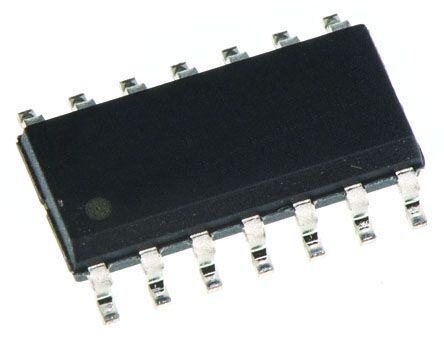
| 描述 | IC OSC TIMER DUAL 100KHZ 14SOIC计时器和支持产品 DUAL PRECISION TIMER |
| 产品分类 | |
| 品牌 | Texas Instruments |
| 产品手册 | http://www.ti.com/litv/slfs023g |
| 产品图片 |
|
| rohs | 符合RoHS无铅 / 符合限制有害物质指令(RoHS)规范要求 |
| 产品系列 | 时钟和计时器IC,计时器和支持产品,Texas Instruments NE556DR- |
| 数据手册 | |
| 产品型号 | NE556DR |
| 产品种类 | 计时器和支持产品 |
| 供应商器件封装 | 14-SOIC |
| 其它名称 | 296-26240-2 |
| 内部定时器数量 | 2 |
| 包装 | 带卷 (TR) |
| 单位重量 | 129.400 mg |
| 商标 | Texas Instruments |
| 安装类型 | 表面贴装 |
| 安装风格 | SMD/SMT |
| 封装 | Reel |
| 封装/外壳 | 14-SOIC(0.154",3.90mm 宽) |
| 封装/箱体 | SOIC-14 |
| 工作温度 | 0°C ~ 70°C |
| 工厂包装数量 | 2500 |
| 最大工作温度 | + 70 C |
| 最小工作温度 | 0 C |
| 标准包装 | 2,500 |
| 电压-电源 | 4.5 V ~ 16 V |
| 电流-电源 | 20mA |
| 电源电压-最大 | 16 V |
| 电源电压-最小 | 4.5 V |
| 电源电流 | 4000 uA |
| 类型 | 555 型,计时器/振荡器(双路) |
| 系列 | NE556 |
| 计数 | - |
| 频率 | 100kHz |


- 商务部:美国ITC正式对集成电路等产品启动337调查
- 曝三星4nm工艺存在良率问题 高通将骁龙8 Gen1或转产台积电
- 太阳诱电将投资9.5亿元在常州建新厂生产MLCC 预计2023年完工
- 英特尔发布欧洲新工厂建设计划 深化IDM 2.0 战略
- 台积电先进制程称霸业界 有大客户加持明年业绩稳了
- 达到5530亿美元!SIA预计今年全球半导体销售额将创下新高
- 英特尔拟将自动驾驶子公司Mobileye上市 估值或超500亿美元
- 三星加码芯片和SET,合并消费电子和移动部门,撤换高东真等 CEO
- 三星电子宣布重大人事变动 还合并消费电子和移动部门
- 海关总署:前11个月进口集成电路产品价值2.52万亿元 增长14.8%


PDF Datasheet 数据手册内容提取
NA556, NE556, SA556, SE556 DUAL PRECISION TIMERS www.ti.com SLFS023G–APRIL1978–REVISEDJUNE2006 FEATURES NA556...D OR N PACKAGE • TwoPrecisionTimingCircuitsPerPackage NE556...D,N,OR NS PACKAGE • AstableorMonostableOperation SA556...D OR NPACKAGE SE556...J PACKAGE • TTL-CompatibleOutputCanSinkorSource (TOPVIEW) upto150mA • ActivePulluporPulldown 1DISCH 1 14 VCC • DesignedtoBeInterchangeableWith 1THRES 2 13 2DISCH SigneticsNE556,SA556,andSE556 1CONT 3 12 2THRES 1RESET 4 11 2CONT APPLICATIONS 1OUT 5 10 2RESET • PrecisionTimersFromMicrosecondsto 1TRIG 6 9 2OUT Hours GND 7 8 2TRIG • Pulse-ShapingCircuits • Missing-PulseDetectors • Tone-BurstGenerators • Pulse-WidthModulators • Pulse-PositionModulators • SequentialTimers • PulseGenerators • FrequencyDividers • ApplicationTimers • IndustrialControls • Touch-ToneEncoders DESCRIPTION/ORDERING INFORMATION These devices provide two independent timing circuits of the NA555, NE555, SA555, or SE555 type in each package. These circuits can be operated in the astable or the monostable mode with external resistor-capacitor (RC) timing control. The basic timing provided by the RC time constant can be controlled actively by modulating thebiasofthecontrol-voltageinput. The threshold (THRES) and trigger (TRIG) levels normally are two-thirds and one-third, respectively, of V . CC These levels can be altered by using the control voltage (CONT) terminal. When the trigger input falls below trigger level, the flip-flop is set and the output goes high. If the trigger input is above the trigger level and the threshold input is above the threshold level, the flip-flop is reset, and the output is low. The reset (RESET) input can override all other inputs and can be used to initiate a new timing cycle. When RESET goes low, the flip-flop is reset and the output goes low. When the output is low, a low-impedance path is provided between the discharge(DISCH)terminalandground(GND). Pleasebeawarethatanimportantnoticeconcerningavailability,standardwarranty,anduseincriticalapplicationsofTexas Instrumentssemiconductorproductsanddisclaimerstheretoappearsattheendofthisdatasheet. PRODUCTIONDATAinformationiscurrentasofpublicationdate. Copyright©1978–2006,TexasInstrumentsIncorporated Products conform to specifications per the terms of the Texas On products compliant to MIL-PRF-38535, all parameters are Instruments standard warranty. Production processing does not testedunlessotherwisenoted.Onallotherproducts,production necessarilyincludetestingofallparameters. processingdoesnotnecessarilyincludetestingofallparameters.
NA556, NE556, SA556, SE556 DUAL PRECISION TIMERS www.ti.com SLFS023G–APRIL1978–REVISEDJUNE2006 ORDERINGINFORMATION V (MAX) T T PACKAGE(1) ORDERABLEPARTNUMBER TOP-SIDEMARKING A V =15V CC PDIP–N Tubeof25 NE556N NE556N Tubeof50 NE556D 0(cid:176) Cto70(cid:176) C 11.2V SOIC–D NE556 Reelof2500 NE556DR SOP–NS Reelof2000 NE556NSR NE556 –40(cid:176) Cto85(cid:176) C 11.2V PDIP–N Tubeof25 SA556N SA556N PDIP–N Tubeof25 NA556N NA556N –40(cid:176) Cto105(cid:176) C 11.2V Tubeof50 NA556D SOIC–D NA556 Reelof2500 NA556DR SE556J SE556J –55(cid:176) Cto125(cid:176) C 10.6V CDIP–J Tubeof25 SE556JB SE556JB (1) Packagedrawings,standardpackingquantities,thermaldata,symbolization,andPCBdesignguidelinesareavailableat www.ti.com/sc/package. FUNCTIONTABLE (eachtimer) TRIGGER THRESHOLD DISCHARGE RESET OUTPUT VOLTAGE(1) VOLTAGE(1) SWITCH Low Irrelevant Irrelevant Low On High <1/3V Irrelevant High Off DD High >1/3V >2/3V Low On DD DD High >1/3V <2/3V Aspreviouslyestablished DD DD (1) Voltagelevelsshownarenominal. FUNCTIONALBLOCKDIAGRAM,EACHTIMER VCC RESET THRES OUT CONT TRIG DISCH GND RESET can overrideTRIG,which can overrideTHRES. 2 SubmitDocumentationFeedback
NA556, NE556, SA556, SE556 DUAL PRECISION TIMERS www.ti.com SLFS023G–APRIL1978–REVISEDJUNE2006 Absolute Maximum Ratings(1) overoperatingfree-airtemperaturerange(unlessotherwisenoted) MIN MAX UNIT V Supplyvoltage(2) 18 V CC V Inputvoltage CONT,RESET,THRES,andTRIG V V I CC I Outputcurrent – 225 mA O Dpackage 86 q Packagethermalimpedance(3)(4) Npackage 80 (cid:176) C/W JA NSpackage 76 q Packagethermalimpedance(5)(6) Jpackage 15.05 (cid:176) C/W JC T Operatingvirtualjunctiontemperature 150 (cid:176) C J Leadtemperature1,6mm(1/16in)fromcasefor60s Jpackage 300 (cid:176) C Leadtemperature1,6mm(1/16in)fromcasefor10s D,N,orNSpackage 260 (cid:176) C T Storagetemperaturerange –65 150 (cid:176) C stg (1) Stressesbeyondthoselistedunder"absolutemaximumratings"maycausepermanentdamagetothedevice.Thesearestressratings only,andfunctionaloperationofthedeviceattheseoranyotherconditionsbeyondthoseindicatedunder"recommendedoperating conditions"isnotimplied.Exposuretoabsolute-maximum-ratedconditionsforextendedperiodsmayaffectdevicereliability. (2) Allvoltagevaluesarewithrespecttonetworkgroundterminal. (3) MaximumpowerdissipationisafunctionofT(max),q ,andT .Themaximumallowablepowerdissipationatanyallowableambient J JA A temperatureisP =(T(max)–T )/q .OperatingattheabsolutemaximumT of150(cid:176) Ccanaffectreliability. D J A JA J (4) ThepackagethermalimpedanceiscalculatedinaccordancewithJESD51-7. (5) MaximumpowerdissipationisafunctionofT(max),q ,andT .Themaximumallowablepowerdissipationatanyallowablecase J JC C temperatureisP =(T(max)–T )/q .OperatingattheabsolutemaximumT of150(cid:176) Ccanaffectreliability. D J C JC J (6) ThepackagethermalimpedanceiscalculatedinaccordancewithMIL-STD-883. Recommended Operating Conditions MIN MAX UNIT NA556,NE556,SA556 4.5 16 V Supplyvoltage V CC SE556 4.5 18 V Inputvoltage CONT,RESET,THRES,andTRIG V V I CC I Outputcurrent – 200 mA O NA556 –40 105 NE556 0 70 T Operatingfree-airtemperature (cid:176) C A SA556 –40 85 SE556 –55 125 SubmitDocumentationFeedback 3
NA556, NE556, SA556, SE556 DUAL PRECISION TIMERS www.ti.com SLFS023G–APRIL1978–REVISEDJUNE2006 Electrical Characteristics V =5Vto15V,T =25(cid:176) C(unlessotherwisenoted) CC A NA556 NE556 SE556 PARAMETER TESTCONDITIONS SA556 UNIT MIN TYP MAX MIN TYP MAX Thresholdvoltage VCC=15V 8.8 10 11.2 9.4 10 10.6 V V T level V =5V 2.4 3.3 4.2 2.7 3.3 4 CC I Thresholdcurrent(1) 30 250 30 250 nA T 4.5 5 5.6 4.8 5 5.2 V =15V CC T =–55(cid:176) Cto125(cid:176) C 3 6 A V Triggervoltagelevel V TRIG 1.1 1.67 2.2 1.45 1.67 1.9 V =5V CC T =–55(cid:176) Cto125(cid:176) C 1.9 A I Triggercurrent TRIGat0V 0.5 2 0.5 0.9 m A TRIG 0.3 0.7 1 0.3 0.7 1 V Resetvoltagelevel V RESET T =–55(cid:176) Cto125(cid:176) C 1.1 A RESETatV 0.1 0.4 0.1 0.4 CC I Resetcurrent mA RESET RESETat0V –0.4 1.5 –0.4 –1 Dischargeswitch I 20 100 20 100 nA DISCH off-statecurrent 9 10 11 9.6 10 10.4 V =15V Controlvoltage CC TA=–55(cid:176) Cto125(cid:176) C 9.6 10.4 V V CONT (opencircuit) 2.6 3.3 4 2.9 3.3 3.8 V =5V CC T =–55(cid:176) Cto125(cid:176) C 2.9 3.8 A V =15V, 0.1 0.25 0.1 0.15 CC IOL=10mA TA=–55(cid:176) Cto125(cid:176) C 0.2 V =15V, 0.4 0.75 0.4 0.5 CC IOL=50mA TA=–55(cid:176) Cto125(cid:176) C 1 V =15V, 2 2.5 2 2.2 CC V Low-level IOL=100mA TA=–55(cid:176) Cto125(cid:176) C 2.7 V OL outputvoltage V =15V,I =200mA 2.5 2.5 CC OL VCC=5V, T =–55(cid:176) Cto125(cid:176) C 0.35 I =3.5mA A OL V =5V, 0.1 0.25 0.1 0.15 CC IOL=5mA TA=–55(cid:176) Cto125(cid:176) C 0.8 V =5V,I =8mA 0.15 0.3 0.15 0.25 CC OL V =15V, 12.75 13.3 13 13.3 CC IOH=–100mA TA=–55(cid:176) Cto125(cid:176) C 12 High-level V V =15V,I =–200mA 12.5 12.5 V OH outputvoltage CC OH V =5V, 2.75 3.3 3 3.3 CC IOH=–100mA TA=–55(cid:176) Cto125(cid:176) C 2 Outputlow, VCC=15V 20 30 20 24 Noload V =5V 6 12 6 10 CC I Supplycurrent mA CC Outputhigh, VCC=15V 18 26 18 20 Noload V =5V 4 10 4 8 CC (1) ThisparameterinfluencesthemaximumvalueofthetimingresistorsRandR inthecircuitofFigure1.Forexample,whenV =5V, B CC themaximumvalueisR=R +R » 3.4MW ,andforV =15V,themaximumvalueis» 10MW . A B CC 4 SubmitDocumentationFeedback
NA556, NE556, SA556, SE556 DUAL PRECISION TIMERS www.ti.com SLFS023G–APRIL1978–REVISEDJUNE2006 Operating Characteristics V =5Vand15V CC NA556 TEST NE556 SE556 PARAMETER CONDITIONS(1) SA556 UNIT MIN TYP MAX MIN TYP MAX Eachtimer, 1 3 0.5 1.5(4) monostable(3) Initialerroroftiming T =25(cid:176) C interval(2) Eachtimer,astable(5) A 2.25% 1.5% Timer1–Timer2 – 1 – 0.5 Eachtimer, 50 30 100(4) Temperature monostable(3) coefficientoftiming T =MINtoMAX ppm/(cid:176) C Eachtimer,astable(5) A 150 90 interval Timer1–Timer2 – 10 – 10 Eachtimer, 0.1 0.5 0.05 0.2(4) Supplyvoltage monostable(3) sensitivityoftiming T =25(cid:176) C %/V Eachtimer,astable(5) A 0.3 0.15 interval Timer1–Timer2 – 0.2 – 0.1 C =15pF, Output-pulserisetime TL=25(cid:176) C 100 300 100 200(4) ns A C =15pF, Output-pulsefalltime TL=25(cid:176) C 100 300 100 200(4) ns A (1) ForconditionsshownasMINorMAX,usetheappropriatevaluespecifiedunderrecommendedoperatingconditions. (2) Timing-intervalerrorisdefinedasthedifferencebetweenthemeasuredvalueandtheaveragevalueofarandomsamplefromeach processrun. (3) ValuesspecifiedareforadeviceinamonostablecircuitsimilartoFigure2,withthefollowingcomponentvalues:R =2kW to100kW , A C=0.1m F. (4) OnproductscomplianttoMIL-PRF-38535,thisparameterisnotproductiontested. (5) ValuesspecifiedareforadeviceinanastablecircuitsimilartoFigure1,withthefollowingcomponentvalues:R =1kW to100kW , A C=0.1m F. SubmitDocumentationFeedback 5
NA556, NE556, SA556, SE556 DUAL PRECISION TIMERS www.ti.com SLFS023G–APRIL1978–REVISEDJUNE2006 APPLICATION INFORMATION VCC VCC (5V to 15V) (5V to 15V) Open (see Note A) 0.01 µF RA CONT VCC RA CONT VCC RESET RL DISCH RESET RL OUT OUT DISCH RB OUT OUT THRES TRIG THRES GND Input TRIG GND C C NOTE A: Bypassing the control-voltage input to ground with a capacitor might improve operation.This should be evaluated for individual applications. Figure1.CircuitforAstableOperation Figure2.CircuitforMonostableOperation 6 SubmitDocumentationFeedback
PACKAGE OPTION ADDENDUM www.ti.com 6-Feb-2020 PACKAGING INFORMATION Orderable Device Status Package Type Package Pins Package Eco Plan Lead/Ball Finish MSL Peak Temp Op Temp (°C) Device Marking Samples (1) Drawing Qty (2) (6) (3) (4/5) JM38510/10902BCA ACTIVE CDIP J 14 1 TBD Call TI N / A for Pkg Type -55 to 125 JM38510 /10902BCA M38510/10902BCA ACTIVE CDIP J 14 1 TBD Call TI N / A for Pkg Type -55 to 125 JM38510 /10902BCA NA556D ACTIVE SOIC D 14 50 Green (RoHS NIPDAU Level-1-260C-UNLIM -40 to 105 NA556 & no Sb/Br) NA556DR ACTIVE SOIC D 14 2500 Green (RoHS NIPDAU Level-1-260C-UNLIM -40 to 105 NA556 & no Sb/Br) NA556N ACTIVE PDIP N 14 25 Green (RoHS NIPDAU N / A for Pkg Type -40 to 105 NA556N & no Sb/Br) NE556D ACTIVE SOIC D 14 50 Green (RoHS NIPDAU Level-1-260C-UNLIM 0 to 70 NE556 & no Sb/Br) NE556DBR ACTIVE SSOP DB 14 2000 Green (RoHS NIPDAU Level-1-260C-UNLIM 0 to 70 N556 & no Sb/Br) NE556DR ACTIVE SOIC D 14 2500 Green (RoHS NIPDAU Level-1-260C-UNLIM 0 to 70 NE556 & no Sb/Br) NE556DRE4 ACTIVE SOIC D 14 2500 Green (RoHS NIPDAU Level-1-260C-UNLIM 0 to 70 NE556 & no Sb/Br) NE556DRG4 ACTIVE SOIC D 14 2500 Green (RoHS NIPDAU Level-1-260C-UNLIM 0 to 70 NE556 & no Sb/Br) NE556N ACTIVE PDIP N 14 25 Green (RoHS NIPDAU N / A for Pkg Type 0 to 70 NE556N & no Sb/Br) NE556NE4 ACTIVE PDIP N 14 25 Green (RoHS NIPDAU N / A for Pkg Type 0 to 70 NE556N & no Sb/Br) NE556NSR ACTIVE SO NS 14 2000 Green (RoHS NIPDAU Level-1-260C-UNLIM 0 to 70 NE556 & no Sb/Br) SA556N ACTIVE PDIP N 14 25 Green (RoHS NIPDAU N / A for Pkg Type -40 to 85 SA556N & no Sb/Br) SA556NE4 ACTIVE PDIP N 14 25 Green (RoHS NIPDAU N / A for Pkg Type -40 to 85 SA556N & no Sb/Br) SE556J ACTIVE CDIP J 14 1 TBD Call TI N / A for Pkg Type -55 to 125 SE556J SE556JB ACTIVE CDIP J 14 1 TBD Call TI N / A for Pkg Type -55 to 125 SE556JB Addendum-Page 1
PACKAGE OPTION ADDENDUM www.ti.com 6-Feb-2020 (1) The marketing status values are defined as follows: ACTIVE: Product device recommended for new designs. LIFEBUY: TI has announced that the device will be discontinued, and a lifetime-buy period is in effect. NRND: Not recommended for new designs. Device is in production to support existing customers, but TI does not recommend using this part in a new design. PREVIEW: Device has been announced but is not in production. Samples may or may not be available. OBSOLETE: TI has discontinued the production of the device. (2) RoHS: TI defines "RoHS" to mean semiconductor products that are compliant with the current EU RoHS requirements for all 10 RoHS substances, including the requirement that RoHS substance do not exceed 0.1% by weight in homogeneous materials. Where designed to be soldered at high temperatures, "RoHS" products are suitable for use in specified lead-free processes. TI may reference these types of products as "Pb-Free". RoHS Exempt: TI defines "RoHS Exempt" to mean products that contain lead but are compliant with EU RoHS pursuant to a specific EU RoHS exemption. Green: TI defines "Green" to mean the content of Chlorine (Cl) and Bromine (Br) based flame retardants meet JS709B low halogen requirements of <=1000ppm threshold. Antimony trioxide based flame retardants must also meet the <=1000ppm threshold requirement. (3) MSL, Peak Temp. - The Moisture Sensitivity Level rating according to the JEDEC industry standard classifications, and peak solder temperature. (4) There may be additional marking, which relates to the logo, the lot trace code information, or the environmental category on the device. (5) Multiple Device Markings will be inside parentheses. Only one Device Marking contained in parentheses and separated by a "~" will appear on a device. If a line is indented then it is a continuation of the previous line and the two combined represent the entire Device Marking for that device. (6) Lead/Ball Finish - Orderable Devices may have multiple material finish options. Finish options are separated by a vertical ruled line. Lead/Ball Finish values may wrap to two lines if the finish value exceeds the maximum column width. Important Information and Disclaimer:The information provided on this page represents TI's knowledge and belief as of the date that it is provided. TI bases its knowledge and belief on information provided by third parties, and makes no representation or warranty as to the accuracy of such information. Efforts are underway to better integrate information from third parties. TI has taken and continues to take reasonable steps to provide representative and accurate information but may not have conducted destructive testing or chemical analysis on incoming materials and chemicals. TI and TI suppliers consider certain information to be proprietary, and thus CAS numbers and other limited information may not be available for release. In no event shall TI's liability arising out of such information exceed the total purchase price of the TI part(s) at issue in this document sold by TI to Customer on an annual basis. Addendum-Page 2
PACKAGE MATERIALS INFORMATION www.ti.com 20-Dec-2018 TAPE AND REEL INFORMATION *Alldimensionsarenominal Device Package Package Pins SPQ Reel Reel A0 B0 K0 P1 W Pin1 Type Drawing Diameter Width (mm) (mm) (mm) (mm) (mm) Quadrant (mm) W1(mm) NA556DR SOIC D 14 2500 330.0 16.4 6.5 9.0 2.1 8.0 16.0 Q1 NE556DR SOIC D 14 2500 330.0 16.4 6.5 9.0 2.1 8.0 16.0 Q1 NE556NSR SO NS 14 2000 330.0 16.4 8.2 10.5 2.5 12.0 16.0 Q1 PackMaterials-Page1
PACKAGE MATERIALS INFORMATION www.ti.com 20-Dec-2018 *Alldimensionsarenominal Device PackageType PackageDrawing Pins SPQ Length(mm) Width(mm) Height(mm) NA556DR SOIC D 14 2500 367.0 367.0 38.0 NE556DR SOIC D 14 2500 367.0 367.0 38.0 NE556NSR SO NS 14 2000 367.0 367.0 38.0 PackMaterials-Page2
None
PACKAGE OUTLINE J0014A CDIP - 5.08 mm max height SCALE 0.900 CERAMIC DUAL IN LINE PACKAGE PIN 1 ID A 4X .005 MIN (OPTIONAL) [0.13] .015-.060 TYP [0.38-1.52] 1 14 12X .100 [2.54] 14X .014-.026 14X .045-.065 [0.36-0.66] [1.15-1.65] .010 [0.25] C A B .754-.785 [19.15-19.94] 7 8 B .245-.283 .2 MAX TYP .13 MIN TYP [6.22-7.19] [5.08] [3.3] SEATING PLANE C .308-.314 [7.83-7.97] AT GAGE PLANE .015 GAGE PLANE [0.38] 0 -15 14X .008-.014 TYP [0.2-0.36] 4214771/A 05/2017 NOTES: 1. All controlling linear dimensions are in inches. Dimensions in brackets are in millimeters. Any dimension in brackets or parenthesis are for reference only. Dimensioning and tolerancing per ASME Y14.5M. 2. This drawing is subject to change without notice. 3. This package is hermitically sealed with a ceramic lid using glass frit. 4. Index point is provided on cap for terminal identification only and on press ceramic glass frit seal only. 5. Falls within MIL-STD-1835 and GDIP1-T14. www.ti.com
EXAMPLE BOARD LAYOUT J0014A CDIP - 5.08 mm max height CERAMIC DUAL IN LINE PACKAGE (.300 ) TYP [7.62] SEE DETAIL B SEE DETAIL A 1 14 12X (.100 ) [2.54] SYMM 14X ( .039) [1] 7 8 SYMM LAND PATTERN EXAMPLE NON-SOLDER MASK DEFINED SCALE: 5X .002 MAX (.063) [0.05] [1.6] METAL ALL AROUND ( .063) SOLDER MASK [1.6] OPENING METAL .002 MAX SOLDER MASK (R.002 ) TYP [0.05] OPENING [0.05] ALL AROUND DETAIL A DETAIL B SCALE: 15X 13X, SCALE: 15X 4214771/A 05/2017 www.ti.com
None
None
None
MECHANICAL DATA MSSO002E – JANUARY 1995 – REVISED DECEMBER 2001 DB (R-PDSO-G**) PLASTIC SMALL-OUTLINE 28 PINS SHOWN 0,38 0,65 0,15 M 0,22 28 15 0,25 0,09 5,60 8,20 5,00 7,40 Gage Plane 1 14 0,25 A 0°–(cid:1)8° 0,95 0,55 Seating Plane 2,00 MAX 0,05 MIN 0,10 PINS ** 14 16 20 24 28 30 38 DIM A MAX 6,50 6,50 7,50 8,50 10,50 10,50 12,90 A MIN 5,90 5,90 6,90 7,90 9,90 9,90 12,30 4040065/E 12/01 NOTES: A. All linear dimensions are in millimeters. B. This drawing is subject to change without notice. C. Body dimensions do not include mold flash or protrusion not to exceed 0,15. D. Falls within JEDEC MO-150 • POST OFFICE BOX 655303 DALLAS, TEXAS 75265
None
IMPORTANTNOTICEANDDISCLAIMER TI PROVIDES TECHNICAL AND RELIABILITY DATA (INCLUDING DATASHEETS), DESIGN RESOURCES (INCLUDING REFERENCE DESIGNS), APPLICATION OR OTHER DESIGN ADVICE, WEB TOOLS, SAFETY INFORMATION, AND OTHER RESOURCES “AS IS” AND WITH ALL FAULTS, AND DISCLAIMS ALL WARRANTIES, EXPRESS AND IMPLIED, INCLUDING WITHOUT LIMITATION ANY IMPLIED WARRANTIES OF MERCHANTABILITY, FITNESS FOR A PARTICULAR PURPOSE OR NON-INFRINGEMENT OF THIRD PARTY INTELLECTUAL PROPERTY RIGHTS. These resources are intended for skilled developers designing with TI products. You are solely responsible for (1) selecting the appropriate TI products for your application, (2) designing, validating and testing your application, and (3) ensuring your application meets applicable standards, and any other safety, security, or other requirements. These resources are subject to change without notice. TI grants you permission to use these resources only for development of an application that uses the TI products described in the resource. Other reproduction and display of these resources is prohibited. No license is granted to any other TI intellectual property right or to any third party intellectual property right. TI disclaims responsibility for, and you will fully indemnify TI and its representatives against, any claims, damages, costs, losses, and liabilities arising out of your use of these resources. TI’s products are provided subject to TI’s Terms of Sale (www.ti.com/legal/termsofsale.html) or other applicable terms available either on ti.com or provided in conjunction with such TI products. TI’s provision of these resources does not expand or otherwise alter TI’s applicable warranties or warranty disclaimers for TI products. Mailing Address: Texas Instruments, Post Office Box 655303, Dallas, Texas 75265 Copyright © 2020, Texas Instruments Incorporated