ICGOO在线商城 > 集成电路(IC) > PMIC - 监控器 > RT9818C-29GV
 Datasheet下载
- 型号: RT9818C-29GV
- 制造商: RICHTEK
- 库位|库存: xxxx|xxxx
- 要求:
| 数量阶梯 | 香港交货 | 国内含税 |
| +xxxx | $xxxx | ¥xxxx |
查看当月历史价格
查看今年历史价格
RT9818C-29GV产品简介:
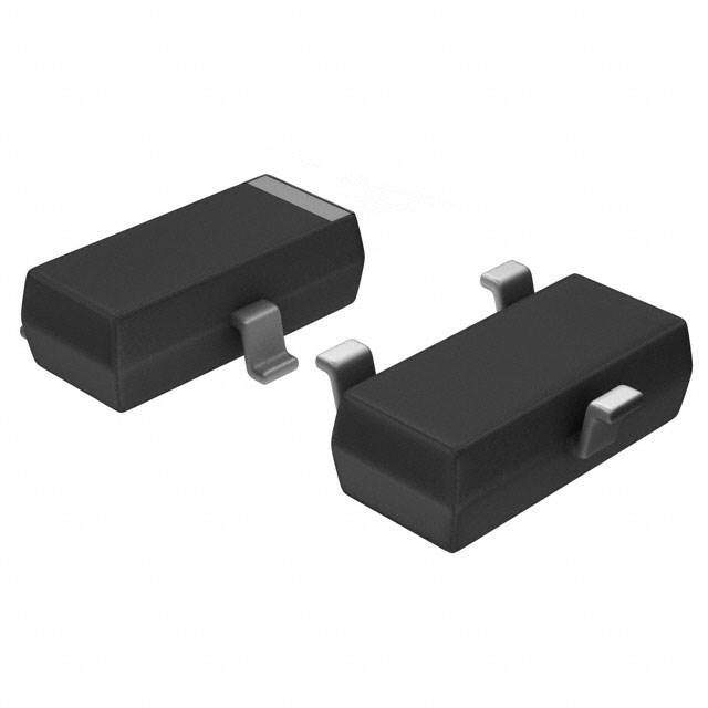
ICGOO电子元器件商城为您提供RT9818C-29GV由RICHTEK设计生产,在icgoo商城现货销售,并且可以通过原厂、代理商等渠道进行代购。 RT9818C-29GV价格参考。RICHTEKRT9818C-29GV封装/规格:PMIC - 监控器, 开路漏极或开路集电极 监控器 1 通道 SOT-23-3。您可以下载RT9818C-29GV参考资料、Datasheet数据手册功能说明书,资料中有RT9818C-29GV 详细功能的应用电路图电压和使用方法及教程。
RT9818C-29GV 是 Richtek(立锜科技)推出的一款 PMIC(电源管理集成电路),属于监控器类别。该型号主要应用于需要精确电压监控和电池保护的场景,例如便携式设备、消费类电子产品以及工业应用。以下是其主要应用场景:

 1. 便携式电子设备
   - 智能手机和平板电脑:用于监测电池电压,确保设备在低电量时及时提醒用户或启动保护机制。
   - 可穿戴设备:如智能手表、健康追踪器等,提供高效的电源管理和电池状态监控。
   - 蓝牙耳机和音箱:实现对小型锂电池的电压检测,防止过充或过放。

 2. 电池管理系统 (BMS)
   - RT9818C-29GV 可作为电池保护电路的一部分,监控单节锂电池或锂离子电池的电压状态,避免因过压或欠压导致电池损坏。
   - 应用于电动工具、无人机、便携式医疗设备等需要电池管理的场景。

 3. 消费类电子产品
   - 便携式充电器(充电宝):监控输入/输出电压,确保安全充电。
   - 游戏手柄和遥控器:提供稳定的电源管理功能,延长电池寿命。

 4. 工业与物联网 (IoT) 设备
   - 传感器节点:为低功耗 IoT 设备提供电压监控功能,确保系统在异常情况下自动断电或报警。
   - 数据采集模块:监测供电电压,保障设备在复杂环境下稳定运行。

 5. 汽车电子
   - 虽然主要用于消费级产品,但在某些轻型汽车电子设备中(如行车记录仪、倒车摄像头),也可以用作电池电压监控解决方案。

 核心特点
- 高精度电压检测:能够准确监测电池电压,支持多种阈值设置。
- 低功耗设计:适合对功耗敏感的应用场景。
- 过压/欠压保护:有效防止电池损坏,提升系统可靠性。

总之,RT9818C-29GV 在任何需要实时电压监控和电池保护的场景中都能发挥重要作用,特别适用于对体积、功耗和成本有严格要求的便携式设备。
| 参数 | 数值 |
| 产品目录 | 集成电路 (IC) |
| 描述 | IC VOLT DETECTOR 2.9V SOT23-3 |
| 产品分类 | |
| 品牌 | Richtek USA Inc |
| 数据手册 | http://www.richtek.com/download_ds.jsp?s=336 |
| 产品图片 |
|
| 产品型号 | RT9818C-29GV |
| rohs | 无铅 / 符合限制有害物质指令(RoHS)规范要求 |
| RoHS指令信息 | http://www.richtek.com/download.jsp?t=UyUyRmFzc2V0cyUyRjIwMDklMkYwNiUyRjE3JTJGcGFnZTY1MTYwenRpeGIucGRmJTNEJTNEJTNE%0AR0w5NTI1LUMtLVBiLWZyZWUrUHJvZHVjdCsrR3JlZW4rUHJvZHVjdCtTdGF0ZW1lbnQrMDkwNjE2%0AQw%3D%3D |
| 产品系列 | - |
| 供应商器件封装 | SOT-23-3 |
| 其它名称 | 1028-1020-1 |
| 包装 | 剪切带 (CT) |
| 受监控电压数 | 1 |
| 复位 | 低有效 |
| 复位超时 | 最小为 143 ms |
| 安装类型 | 表面贴装 |
| 封装/外壳 | TO-236-3,SC-59,SOT-23-3 |
| 工作温度 | -40°C ~ 85°C |
| 标准包装 | 1 |
| 电压-阈值 | 2.9V |
| 类型 | 简单复位/加电复位 |
| 输出 | 开路漏极或开路集电极 |


- 商务部:美国ITC正式对集成电路等产品启动337调查
- 曝三星4nm工艺存在良率问题 高通将骁龙8 Gen1或转产台积电
- 太阳诱电将投资9.5亿元在常州建新厂生产MLCC 预计2023年完工
- 英特尔发布欧洲新工厂建设计划 深化IDM 2.0 战略
- 台积电先进制程称霸业界 有大客户加持明年业绩稳了
- 达到5530亿美元!SIA预计今年全球半导体销售额将创下新高
- 英特尔拟将自动驾驶子公司Mobileye上市 估值或超500亿美元
- 三星加码芯片和SET,合并消费电子和移动部门,撤换高东真等 CEO
- 三星电子宣布重大人事变动 还合并消费电子和移动部门
- 海关总署:前11个月进口集成电路产品价值2.52万亿元 增长14.8%


PDF Datasheet 数据手册内容提取
® RT9818 Micro-Power Voltage Detectors General Description Features The RT9818 is a micro-power voltage detector supervising Internally Fixed Threshold 1.2V to 5V in 0.1V Step the power supply voltage level for microprocessors (μP) High Accuracy ±±±±±1.5% or digital systems. It provides internally fixed threshold Low Supply Current 3μμμμμA levels with 0.1V per step ranging from 1.2V to 5V, which No External Components Required covers most digital applications. It features low supply Quick Reset within 20μμμμμs current of 3μA. The RT9818 performs supervisory function Built-In Recovery Delay Include 0ms, 55ms, 220ms, by sending out a reset signal whenever the V voltage 450ms Options DD falls below a preset threshold level. This reset signal will Low Functional Supply Voltage 0.9V last the whole period before VDD recovering. Once VDD N-Channel Open-Drain Output recovered upcrossing the threshold level, the reset signal Small SC-82, SC-70-3, SOT-23-3, SOT-23-5, SOT-89 will be released after a certain delay time. RT9818 is Packages provided in SC-82, SC-70-3, SOT-23-3, SOT-23-5 and RoHS Compliant and 100% Lead (Pb)-Free SOT-89 packages. Applications Ordering Information Computers RT9818 - Controllers Package Type Intelligent Instruments U3 : SC-70-3 V : SOT-23-3 Critical μP and μC Power Monitoring VL : SOT-23-3 (L-Type) Portable/Battery-Powered Equipment B : SOT-23-5 X : SOT-89 Marking Information Y : SC-82 YR : SC-82 (R-Type) For marking information, contact our sales representative Lead Plating System directly or through a Richtek distributor located in your P : Pb Free G : Green (Halogen Free and Pb Free) area. Threshold Voltage 12 : 1.2V 13 : 1.3V Typical Application Circuit : 49 : 4.9V 50 : 5.0V Reset Active Timeout Period 100k RT9818 A = 0ms (RESET) Pull Up GND B = 55ms (RESET) VDD C = 220ms (RESET) VDD P D = 450ms (RESET) RESET/ E = 0ms (RESET) RESET/ RESET F = 55ms (RESET) RESET G = 220ms (RESET) H = 450ms (RESET) Note : Richtek products are : RoHS compliant and compatible with the current require- ments of IPC/JEDEC J-STD-020. Suitable for use in SnPb or Pb-free soldering processes. Copyright © 2016 Richtek Technology Corporation. All rights reserved. is a registered trademark of Richtek Technology Corporation. DS9818-11 August 2016 www.richtek.com 1
RT9818 Pin Configuration (TOP VIEW) VDD GND NC RESET/ RESET NC 4 3 3 4 3 2 2 2 RESET/ VDD GND RESET/ RESET VDD GND RESET SC-82 SC-82 (R-Type) SC-70-3 VDD VDD NC NC 3 3 5 4 1 2 3 2 2 2 3 RESET/ GND GND RESET/ RESET/ VDDGND RESET/ VDD GND RESET RESET RESET RESET SOT-23-3 SOT-23-3 (L-Type) SOT-23-5 SOT-89 Functional Pin Description Pin Name Pin Function GND Ground. RESET Active low open-drain reset output. RESET Active high open-drain reset output. VDD Power pin. Functional Block Diagram VDD RESET/ RESET CMP Timer N MOS VSET GND Threshold Voltage Setting POR Power On Reset Timing Diagram V DD V TH 0V VRESET Delay Time (0, 55, 220, 450ms) 0V VRESET Delay Time (0, 55, 220, 450ms) 0V Copyright © 2016 Richtek Technology Corporation. All rights reserved. is a registered trademark of Richtek Technology Corporation. www.richtek.com DS9818-11 August 2016 2
RT9818 Absolute Maximum Ratings (Note 1) Terminal Voltage (with Respect to GND) V ----------------------------------------------------------------------------------------------------------------------------- −0.3V to 6V DD All Other Inputs ------------------------------------------------------------------------------------------------------------- −0.3V to 6V Input Current, I ---------------------------------------------------------------------------------------------------------- 20mA VDD Power Dissipation, P @ T = 25°C D A SC-70 / SC-82--------------------------------------------------------------------------------------------------------------- 0.25W SOT-23-3 --------------------------------------------------------------------------------------------------------------------- 0.4W SOT-23-5 --------------------------------------------------------------------------------------------------------------------- 0.4W SOT-89------------------------------------------------------------------------------------------------------------------------ 0.55W Package Thermal Resistance (Note 2) SC-70 / SC-82, θ --------------------------------------------------------------------------------------------------------- 400°C/W JA SOT-23-3, θ ---------------------------------------------------------------------------------------------------------------- 250°C/W JA SOT-23-5, θ ---------------------------------------------------------------------------------------------------------------- 250°C/W JA SOT-89, θ ------------------------------------------------------------------------------------------------------------------ 180°C/W JA Lead Temperature (Soldering, 10sec.)--------------------------------------------------------------------------------- 260°C Storage Temperature Range --------------------------------------------------------------------------------------------- −65°C to 150°C ESD Susceptibility (Note 3) HBM (Human Body Model)----------------------------------------------------------------------------------------------- 2kV Recommended Operating Conditions (Note 4) Junction Temperature Range--------------------------------------------------------------------------------------------- −40°C to 125°C Ambient Temperature Range--------------------------------------------------------------------------------------------- −40°C to 85°C Electrical Characteristics (VDD = 3V, unless otherwise specified) Parameter Symbol Test Conditions Min Typ Max Unit Operating V (V ) Range V 0.9 -- 6 V DD OUT DD Supply Current I V = 3V, V = 4.5V, T = 27C -- 3 8 A DD TH DD A Reset Threshold V T = 27C -- 1.2 to 5 -- V TH A Threshold Voltage Accuracy V T = 27C 1.5 -- 1.5 % TH A V Drop to Reset Delay t Drop = V 125mV -- 20 -- s DD RD TH RT9818A/E -- 0 -- Reset Active RT9818B/F 35 55 75 t V 1.02 x V ms RP DD TH Time Out Period RT9818C/G 143 220 297 RT9818D/H 292 450 608 RESET Output Voltage Low V 3 = V < V I > 3.5mA -- -- 0.4 V (Note 5) OL DD TH SINK Hysteresis Width V -- 0.01V 0.016V V HYS TH TH Copyright © 2016 Richtek Technology Corporation. All rights reserved. is a registered trademark of Richtek Technology Corporation. DS9818-11 August 2016 www.richtek.com 3
RT9818 Note 1. Stresses beyond those listed “Absolute Maximum Ratings” may cause permanent damage to the device. These are stress ratings only, and functional operation of the device at these or any other conditions beyond those indicated in the operational sections of the specifications is not implied. Exposure to absolute maximum rating conditions may affect device reliability. Note 2. θJA is measured at TA= 25°C on a low effective thermal conductivity single-layer test board per JEDEC 51-3. Note 3. Devices are ESD sensitive. Handling precaution is recommended. Note 4. The device is not guaranteed to function outside its operating conditions. Note 5. The voltage VOL can be calculated by VOL = VDD − Ir * R. Where R is the pull-up resistor and Ir is the current flowing through the pull-up resistor. For typical application (R=100kΩ), VOL is less than 0.2V. Copyright © 2016 Richtek Technology Corporation. All rights reserved. is a registered trademark of Richtek Technology Corporation. www.richtek.com DS9818-11 August 2016 4
RT9818 Typical Operating Characteristics Nch Driver Output Current vs. V Nch Driver Output Current vs. V DS DS 2.4 60 RT9818A-12 RT9818C-30 ) 2.0 VDD = 1.1V 50 VDD = 2.8V A m ) rrent ( 1.6 nt (mA 40 VDD = 2.5V u e C 1.2 rr 30 ut Cu VDD = 2V Outp 0.8 VDD = 1V put 20 ut O 0.4 10 VDD = 1.5V 0.0 0 0 0.3 0.6 0.9 1.2 1.5 0 0.5 1 1.5 2 2.5 3 3.5 VDS (V) VDS (V) Nch Driver Output Current vs. V Output Voltage vs. Input Voltage DS 120 7 RT9818A-45 RT9818 100 6 A) V) 5 nt (m 80 age ( 4 urre 60 VDD = 4.4V Volt put C 40 == 43V.5V utput 3 4.5V ut = 3V O 2 O = 2.5V 20 = 2V 1 1.2V = 1.5V 0 0 0 1 2 3 4 5 0 1 2 3 4 5 6 V (V) Input Voltage (V) DS Supply Current vs. Input Voltage Supply Current vs. Input Voltage 6 4.0 RT9818A-12 RT9818C-30 3.5 5 80°C A) A) 3.0 80°C μ μ nt ( 4 nt ( 2.5 e 25°C e 25°C urr 3 urr 2.0 C C y y −30°C pl pl 1.5 up 2 −30°C up S S 1.0 1 0.5 0 0.0 0 1 2 3 4 5 6 0 1 2 3 4 5 6 Input Voltage (V) Input Voltage (V) Copyright © 2016 Richtek Technology Corporation. All rights reserved. is a registered trademark of Richtek Technology Corporation. DS9818-11 August 2016 www.richtek.com 5
RT9818 Supply Current vs. Input Voltage Power Down Reset Delay vs. Temperature 4.0 14 RT9818A-45 RT9818A-12 ) 3.5 µs 12 A) 3.0 80°C ay ( μ 25°C el 10 Current ( 22..05 -30°C Reset D 8 VDROP = 200mV VDROP = 150mV Supply 11..05 r Down 46 VDROP = 250mV e w 0.5 Po 2 0.0 0 0 1 2 3 4 5 6 -50 -25 0 25 50 75 100 125 Input Voltage (V) Temperature (°C) Power Down Reset Delay vs. Temperature Power Down Reset Delay vs. Temperature 45 45 RT9818C-30 RT9818A-45 µs) 40 s) 1 40 ay ( 35 y (µ 35 el a D 30 el 30 eset 25 VDROP = 200mV set D 25 VDROP = 200mV VDROP = 150mV R e n 20 VDROP = 150mV R 20 w n o 15 w 15 D o wer 10 VDROP = 250mV er D 10 VDROP = 250mV o w P 5 o 5 P 0 0 -50 -25 0 25 50 75 100 125 -50 -25 0 25 50 75 100 125 Temperature (°C) Temperature (°C) Reset Threshold Deviation vs. Temperature Nch Driver Sink Current vs. Input Voltage 6 40 RT9818 RT9818C-30, VDS = 0.5V 5V 35 −30°C V) 5 4.5V mA) 30 eshold ( 4 4.2V nt I (SINK 2205 25°C hr e 80°C et T 3 Curr 15 Res 2 2.2V Sink 10 1.2V 5 1 0 -50 -25 0 25 50 75 100 125 0 0.5 1 1.5 2 2.5 3 3.5 Temperature (°C) Input Voltage (V) Copyright © 2016 Richtek Technology Corporation. All rights reserved. is a registered trademark of Richtek Technology Corporation. www.richtek.com DS9818-11 August 2016 6
RT9818 Nch Driver Sink Current vs. Input Voltage Power Up Reset Time-Out vs. Temperature 50 500 RT9818A-45, VDS = 0.5V RT9818C ) s −30°C m mA) 40 25°C Out ( 400 (NK 30 me- 300 VTH = 2.9V nt ISI 80°C et Ti e s urr 20 Re 200 VTH = 3V k C Up Sin 10 er 100 w o P 0 0 0 1 2 3 4 5 -50 -25 0 25 50 75 100 125 Input Voltage (V) Temperature (°C) Power Up Reset Time-Out vs. Temperature Output Delay Time vs. Load Capacitance 100 1000 RT9818A RT9818 ) s µ ut ( 80 ms) 100 et Time-O 60 VTH = 5V ay Time ( 10 s el Re 40 D 1 VTH = 1.2V p VTH = 4.5V ut U p wer 20 Out 0.1 o P VTH = 4.5V 0.01 0 0.0001 0.0010 0.0100 0.1000 1.0000 -50 -25 0 25 50 75 100 125 Temperature (°C) Load Capacitance (µF) Nch Driver Output Current vs. V Nch Driver Output Current vs. Input Voltage DS 160 60 RT9818G-31 RT9818G-31 1 1 A) 140 A) VDS = 0.5V −30°C m m 50 nt ( 120 nt ( 25°C e e Curr 100 VDD = 6V Curr 40 put 80 == 55V.5V put 30 80°C ut = 4.5V ut Driver O 4600 == 43V.5V Driver O 20 ch 20 ch 10 N N 0 0 0 1 2 3 4 5 6 0 1 2 3 4 5 6 V (V) Input Voltage (V) DS Copyright © 2016 Richtek Technology Corporation. All rights reserved. is a registered trademark of Richtek Technology Corporation. DS9818-11 August 2016 www.richtek.com 7
RT9818 Power Down Reset Time-Out vs. Temperature Output Voltage vs. Input Voltage 500 7 s) RT9818G-31 RT9818G-31 m ut ( 400 6 O e- V) 5 m e ( Ti 300 g set olta 4 e V n R 200 put 3 ow Out 2 D r 100 we 1 o P 0 0 -50 -25 0 25 50 75 100 125 0 1 2 3 4 5 6 Temperature (°C) Input Voltage (V) Power Down Reset Time-Out vs. Temperature Threshold Voltage vs. Temperature 30 4.40 s) RT9818G-31 RT9818A-42 µ ut ( 25 1 4.35 -O V) 4.30 me 20 e ( Rising set Ti 15 VDROP = 200mV VDROP = 150mV Voltag 44..2205 Re d Falling n ol 4.15 w 10 h o VDROP = 250mV es D r 4.10 er 5 Th w 4.05 o P 0 4.00 -50 -25 0 25 50 75 100 125 -50 -25 0 25 50 75 100 125 Temperature (°C) Temperature (C) Threshold Voltage vs. Temperature 2.40 RT9818C-22 2.35 1 V) 2.30 e ( g 2.25 Rising a olt V 2.20 d Falling ol 2.15 h s e r 2.10 h T 2.05 2.00 -50 -25 0 25 50 75 100 125 Temperature (C) Copyright © 2016 Richtek Technology Corporation. All rights reserved. is a registered trademark of Richtek Technology Corporation. www.richtek.com DS9818-11 August 2016 8
RT9818 Application Information Multiple Supplies Mainly, the pull-up connected to the RT9818 will connect to the supply voltage that is being monitored at the IC's VDD pin. However, some systems may use the open- drain output to level-shift from the monitored supply to reset circuitry powered by some other supply. Benefits of Highly Accurate Reset Threshold Most μP supervisor ICs have reset threshold voltages between 1% and 1.5% below the value of nominal supply voltages. This ensures a reset will not occur within 1% of the nominal supply, but will occur when the supply is 1.5% below nominal. Copyright © 2016 Richtek Technology Corporation. All rights reserved. is a registered trademark of Richtek Technology Corporation. DS9818-11 August 2016 www.richtek.com 9
RT9818 Outline Dimension H D L C B e A A1 b Dimensions In Millimeters Dimensions In Inches Symbol Min Max Min Max A 0.800 1.100 0.031 0.044 A1 0.000 0.100 0.000 0.004 B 1.150 1.350 0.045 0.054 b 0.150 0.400 0.006 0.016 C 1.800 2.450 0.071 0.096 D 1.800 2.250 0.071 0.089 e 1.300 0.051 H 0.080 0.260 0.003 0.010 L 0.210 0.460 0.008 0.018 SC-70-3 Surface Mount Package Copyright © 2016 Richtek Technology Corporation. All rights reserved. is a registered trademark of Richtek Technology Corporation. www.richtek.com DS9818-11 August 2016 10
RT9818 D H e L C B b b1 A A1 e Dimensions In Millimeters Dimensions In Inches Symbol Min Max Min Max A 0.800 1.100 0.031 0.043 A1 0.000 0.100 0.000 0.004 B 1.150 1.350 0.045 0.053 b 0.150 0.400 0.006 0.016 b1 0.350 0.500 0.014 0.020 C 1.800 2.450 0.071 0.096 D 1.800 2.200 0.071 0.087 e 1.300 0.051 H 0.080 0.260 0.003 0.010 L 0.200 0.460 0.008 0.018 SC-82 Surface Mount Package Copyright © 2016 Richtek Technology Corporation. All rights reserved. is a registered trademark of Richtek Technology Corporation. DS9818-11 August 2016 www.richtek.com 11
RT9818 H D L C B e A A1 b Dimensions In Millimeters Dimensions In Inches Symbol Min Max Min Max A 0.889 1.295 0.035 0.051 A1 0.000 0.152 0.000 0.006 B 1.397 1.803 0.055 0.071 b 0.356 0.508 0.014 0.020 C 2.591 2.997 0.102 0.118 D 2.692 3.099 0.106 0.122 e 1.803 2.007 0.071 0.079 H 0.080 0.254 0.003 0.010 L 0.300 0.610 0.012 0.024 SOT-23-3 Surface Mount Package Copyright © 2016 Richtek Technology Corporation. All rights reserved. is a registered trademark of Richtek Technology Corporation. www.richtek.com DS9818-11 August 2016 12
RT9818 H D L C B b A A1 e Dimensions In Millimeters Dimensions In Inches Symbol Min Max Min Max A 0.889 1.295 0.035 0.051 A1 0.000 0.152 0.000 0.006 B 1.397 1.803 0.055 0.071 b 0.356 0.559 0.014 0.022 C 2.591 2.997 0.102 0.118 D 2.692 3.099 0.106 0.122 e 0.838 1.041 0.033 0.041 H 0.080 0.254 0.003 0.010 L 0.300 0.610 0.012 0.024 SOT-23-5 Surface Mount Package Copyright © 2016 Richtek Technology Corporation. All rights reserved. is a registered trademark of Richtek Technology Corporation. DS9818-11 August 2016 www.richtek.com 13
RT9818 D D1 A B C C1 e e H A b b b1 Dimensions In Millimeters Dimensions In Inches Symbol Min Max Min Max A 1.397 1.600 0.055 0.063 b 0.356 0.483 0.014 0.019 B 2.388 2.591 0.094 0.102 b1 0.406 0.533 0.016 0.021 C 3.937 4.242 0.155 0.167 C1 0.787 1.194 0.031 0.047 D 4.394 4.597 0.173 0.181 D1 1.397 1.753 0.055 0.069 e 1.448 1.549 0.057 0.061 H 0.356 0.432 0.014 0.017 3-Lead SOT-89 Surface Mount Package Richtek Technology Corporation 14F, No. 8, Tai Yuen 1st Street, Chupei City Hsinchu, Taiwan, R.O.C. Tel: (8863)5526789 Richtek products are sold by description only. Richtek reserves the right to change the circuitry and/or specifications without notice at any time. Customers should obtain the latest relevant information and data sheets before placing orders and should verify that such information is current and complete. Richtek cannot assume responsibility for use of any circuitry other than circuitry entirely embodied in a Richtek product. Information furnished by Richtek is believed to be accurate and reliable. However, no responsibility is assumed by Richtek or its subsidiaries for its use; nor for any infringements of patents or other rights of third parties which may result from its use. No license is granted by implication or otherwise under any patent or patent rights of Richtek or its subsidiaries. www.richtek.com DS9818-11 August 2016 14