ICGOO在线商城 > 集成电路(IC) > PMIC - 监控器 > ADM706ANZ
 Datasheet下载
- 型号: ADM706ANZ
- 制造商: Analog
- 库位|库存: xxxx|xxxx
- 要求:
| 数量阶梯 | 香港交货 | 国内含税 |
| +xxxx | $xxxx | ¥xxxx |
查看当月历史价格
查看今年历史价格
ADM706ANZ产品简介:
ICGOO电子元器件商城为您提供ADM706ANZ由Analog设计生产,在icgoo商城现货销售,并且可以通过原厂、代理商等渠道进行代购。 ADM706ANZ价格参考。AnalogADM706ANZ封装/规格:PMIC - 监控器, 推挽式,图腾柱 监控器 1 通道 8-PDIP。您可以下载ADM706ANZ参考资料、Datasheet数据手册功能说明书,资料中有ADM706ANZ 详细功能的应用电路图电压和使用方法及教程。
ADM706ANZ 是由 Analog Devices Inc. 生产的一款电源管理集成电路(PMIC),属于监控器类别。它主要用于监测系统的电压和温度,确保系统在安全范围内运行。

 主要应用场景包括:

1. 工业控制系统:用于监测工业设备的供电电压和温度,防止因电压波动或过热导致的系统故障。
2. 通信设备:在基站、路由器等通信设备中,监控电源状态,保障设备长时间稳定运行。
3. 嵌入式系统与工控主板:用于嵌入式设备中的电源管理和故障检测,提升系统可靠性。
4. 服务器与计算机系统:监控CPU、内存等关键部件的供电情况,提供看门狗定时器功能以防止程序跑飞。
5. 仪器仪表:用于精密仪器中对环境温度和电压变化敏感的部分进行监控。

该芯片具备低功耗、高精度的特点,支持多种电压阈值设定,并具有复位输出、看门狗定时器等功能,适合需要高可靠性的应用场景。
| 参数 | 数值 |
| 产品目录 | 集成电路 (IC)半导体 |
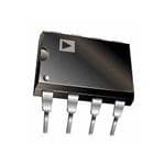
| 描述 | IC SUPERVISOR MPU 4.40V WD 8DIP监控电路 3V VTG Monitor MPU |
| 产品分类 | |
| 品牌 | Analog Devices |
| 产品手册 | |
| 产品图片 |
|
| rohs | 符合RoHS无铅 / 符合限制有害物质指令(RoHS)规范要求 |
| 产品系列 | 电源管理 IC,监控电路,Analog Devices ADM706ANZ- |
| NumberofInputsMonitored | 1 Input |
| 数据手册 | |
| 产品型号 | ADM706ANZ |
| 产品培训模块 | http://www.digikey.cn/PTM/IndividualPTM.page?site=cn&lang=zhs&ptm=25511 |
| 产品目录页面 | |
| 产品种类 | 监控电路 |
| 人工复位 | Manual Reset |
| 供应商器件封装 | 8-PDIP |
| 功率失效检测 | Yes |
| 包装 | 管件 |
| 受监控电压数 | 1 |
| 商标 | Analog Devices |
| 复位 | 低有效 |
| 复位超时 | 最小为 160 ms |
| 安装类型 | 通孔 |
| 安装风格 | Through Hole |
| 封装 | Tube |
| 封装/外壳 | 8-DIP(0.300",7.62mm) |
| 封装/箱体 | PDIP-8 |
| 工作温度 | -40°C ~ 85°C |
| 工作电源电流 | 250 uA |
| 工厂包装数量 | 50 |
| 最大功率耗散 | 727 mW |
| 最大工作温度 | + 85 C |
| 最小工作温度 | - 40 C |
| 标准包装 | 50 |
| 欠电压阈值 | 4.25 V |
| 电压-阈值 | 4.4V |
| 电池备用开关 | No Backup |
| 电源电压-最大 | 5.5 V |
| 电源电压-最小 | 4.75 V |
| 监视器 | Watchdog |
| 类型 | Voltage Supervisory |
| 系列 | ADM706 |
| 芯片启用信号 | No Chip Enable |
| 被监测输入数 | 1 Input |
| 输出 | 推挽式,图腾柱 |
| 输出类型 | Active Low, Push-Pull |
| 过电压阈值 | 4.5 V |
| 重置延迟时间 | 280 ms |
| 阈值电压 | 4.4 V |


- 商务部:美国ITC正式对集成电路等产品启动337调查
- 曝三星4nm工艺存在良率问题 高通将骁龙8 Gen1或转产台积电
- 太阳诱电将投资9.5亿元在常州建新厂生产MLCC 预计2023年完工
- 英特尔发布欧洲新工厂建设计划 深化IDM 2.0 战略
- 台积电先进制程称霸业界 有大客户加持明年业绩稳了
- 达到5530亿美元!SIA预计今年全球半导体销售额将创下新高
- 英特尔拟将自动驾驶子公司Mobileye上市 估值或超500亿美元
- 三星加码芯片和SET,合并消费电子和移动部门,撤换高东真等 CEO
- 三星电子宣布重大人事变动 还合并消费电子和移动部门
- 海关总署:前11个月进口集成电路产品价值2.52万亿元 增长14.8%


PDF Datasheet 数据手册内容提取
3 V, Voltage Monitoring Microprocessor Supervisory Circuits Data Sheet ADM706P/ADM706R/ADM706S/ADM706T, ADM708R/ADM708S/ADM708T FEATURES FUNCTIONAL BLOCK DIAGRAMS Precision supply voltage monitor 2.63 V (ADM706P, ADM706R, ADM708R) WATCHDOG WATCHDOG WATCHDOG INPUT (WDI) TRANSITION TIMER WATCHDOG 2.93 V (ADM706S, ADM708S) DETECTOR OUTPUT (WDO) 3.08 V (ADM706T, ADM708T) VCC RESETAND 100 µA quiescent current WATCHDOG TIMEBASE 200 ms reset pulse width 70μA Debounced manual reset input (MR) MR RESET RESET, Independent watchdog timer GENERATOR (P = RESET) VCC 1.6 sec timeout (ADM706P, ADM706R, ADM706S, VREF* ADM706P/ADM706R/ ADM706T) POWER-FAIL ADM706S/ADM706T Reset output INPUT (PFI) POWER-FAIL 1.25V OUTPUT (PFO) AAccttiivvee lhoiwgh ( A(ADDMM770066RP, )A DM706S, ADM706T) *VOLTAGE REFERENCE = 2.63V (P/R), 2.93V (S), 3.08V (T) 06435-001 Both active high and active low (ADM708R, ADM708S, Figure 1. ADM706P/ADM706R/ADM706S/ADM706T ADM708T) Voltage monitor for power fail or low battery warning VCC Guaranteed RESET valid with V = 1 V 70μA RESET CC Superior upgrade for MAX706P/R/S/T, MAX708R/S/T MR RESET RESET GENERATOR VCC APPLICATIONS VREF* ADM708R/ADM708S/ Microprocessor systems POWER-FAIL ADM708T INPUT (PFI) POWER-FAIL Computers 1.25V OUTPUT (PFO) CInotnetllrioglelenrts i nstruments *VOLTAGE REFERENCE = 2.63V (R), 2.93V (S), 3.08V (T) 06435-002 Figure 2. ADM708R/ADM708S/ADM708T Critical microprocessor monitoring Battery operated systems Portable instruments GENERAL DESCRIPTION The ADM706P/ADM706R/ADM706S/ADM706T and the The ADM706R, ADM706S, and ADM706T are identical except ADM708R/ADM708S/ADM708T microprocessor supervisory for the reset threshold monitor levels, which are 2.63 V, 2.93 V, and circuits are suitable for monitoring either 3 V or 3.3 V power 3.08 V, respectively. The ADM706P is identical to the ADM706R supplies. in that the reset threshold is 2.63 V. It differs only in that it has an active high reset output. The ADM706P/ADM706R/ADM706S/ADM706T provide power supply monitoring circuitry that generate a reset output The ADM708R/ADM708S/ADM708T provide similar functio- during power-up, power-down, and brownout conditions. The nality as the ADM706R/ADM706S/ADM706T and only differ reset output remains operational with V as low as 1 V. in that a watchdog timer function is not available. Instead, an CC Independent watchdog monitoring circuitry is also provided. This active high reset output (RESET) is provided in addition to the activates if the watchdog input does not toggle within 1.6 sec. active low (RESET) output. In addition, there is a 1.25 V threshold detector for a power fail All devices are available in narrow 8-lead PDIP and 8-lead warning, low battery detection, or to monitor an additional SOIC packages. power supply. An active low debounced MR input is also included. Rev. E Document Feedback Information furnished by Analog Devices is believed to be accurate and reliable. However, no responsibility is assumed by Analog Devices for its use, nor for any infringements of patents or other One Technology Way, P.O. Box 9106, Norwood, MA 02062-9106, U.S.A. rights of third parties that may result from its use. Specifications subject to change without notice. No license is granted by implication or otherwise under any patent or patent rights of Analog Devices. Tel: 781.329.4700 ©2007–2016 Analog Devices, Inc. All rights reserved. Trademarks and registered trademarks are the property of their respective owners. Technical Support www.analog.com
ADM706P/ADM706R/ADM706S/ADM706T, ADM708R/ADM708S/ADM708T Data Sheet TABLE OF CONTENTS Features .............................................................................................. 1 Manual Reset ............................................................................... 10 Applications ....................................................................................... 1 Watchdog Timer (ADM706P/ADM706R/ Functional Block Diagrams ............................................................. 1 ADM706S/ADM706T) .............................................................. 10 General Description ......................................................................... 1 Power Fail Comparator .............................................................. 11 Revision History ............................................................................... 2 Adding Hysteresis to the Power Fail Comparator ................. 11 Specifications ..................................................................................... 3 Valid RESET Below 1 V VCC ..................................................... 11 Absolute Maximum Ratings ............................................................ 5 Applications Information .............................................................. 12 ESD Caution .................................................................................. 5 Monitoring Additional Supply Levels ...................................... 12 Pin Configurations and Function Descriptions ........................... 6 Microprocessors with Bidirectional RESET ........................... 12 Typical Performance Characteristics ............................................. 8 Outline Dimensions ....................................................................... 13 Circuit Information ........................................................................ 10 Ordering Guide .......................................................................... 14 Power Fail Reset .......................................................................... 10 REVISION HISTORY 1/16—Rev. D to Rev. E 5/08—Rev. B to Rev. C Changes to Table 3 ............................................................................ 6 Changes to Applications Section ..................................................... 1 Changes to Table 4 ............................................................................ 7 Changes to Table 2 ............................................................................. 5 Changes to Power Fail Comparator Section, Figure 17, Changes to Table 3 ............................................................................. 6 and Figure 18 ................................................................................... 10 Changes to Figure 8 ........................................................................... 7 Changes to Figure 20 and Figure 22 ............................................. 12 Changes to Figure 16 ......................................................................... 9 Changes to Ordering Guide .......................................................... 14 2/07—Rev. A to Rev. B 10/14—Rev. C to Rev. D Updated Format .................................................................. Universal Changes to Pin 4 Description; Table 3 ........................................... 6 Changes to Table 1 ............................................................................. 3 Changes to Pin 4 Description; Table 4 ........................................... 7 Updated Outline Dimensions ....................................................... 12 Changes to Ordering Guide .......................................................... 14 Changes to Ordering Guide .......................................................... 13 Rev. E | Page 2 of 16
Data Sheet ADM706P/ADM706R/ADM706S/ADM706T, ADM708R/ADM708S/ADM708T SPECIFICATIONS V = 2.70 V to 5.5 V (ADM706P/ADM706R/ADM708R), V = 3.00 V to 5.5 V (ADM70xS), V = 3.15 V to 5.5 V (ADM70xT), T = CC CC CC A T to T unless otherwise noted. MIN MAX Table 1. Parameter Min Typ Max Unit Test Conditions/Comments POWER SUPPLY V Operating Voltage Range 1.0 5.5 V CC Supply Current 100 200 μA V < 3.6 V CC 150 350 μA V < 5.5 V CC LOGIC OUTPUT Reset Threshold (V ) 2.55 2.63 2.70 V ADM706P/ADM706R/ADM708R RST 2.85 2.93 3.00 V ADM706S/ADM708S 3.00 3.08 3.15 V ADM706T/ADM708T Reset Threshold Hysteresis 20 mV RESET PULSE WIDTH 160 200 280 ms ADM706P/ADM706R/ADM708R, V = 3 V CC 160 200 280 ms ADM706S/ADM708S/ADM706T/ADM708T, V = 3.3 V CC 200 ms V = 5.0 V CC RESET OUTPUT VOLTAGE (ADM706R/ADM708R/ ADM706S/ADM708S/ADM706T/ADM708T) V 0.8 × V V V (max) < V < 3.6 V, I = 500 μA OH CC RST CC SOURCE V 0.3 V V (max) < V < 3.6 V, I = 1.2 mA OL RST CC SINK V V − 1.5 V V 4.5 V < V < 5.5 V, I = 800 μA OH CC CC SOURCE V 0.4 V 4.5 V < V < 5.5 V, I = 3.2 mA OL CC SINK V 0.3 V V = 1 V, I = 100 μA OL CC SINK RESET OUTPUT VOLTAGE (ADM706P) V V − 0.6 V V V (max) < V < 3.6 V, I = 215 μA OH CC RST CC SOURCE V 0.3 V V (max) < V < 3.6 V, I = 1.2 mA OL RST CC SINK V V − 1.5 V V 4.5 V < V < 5.5 V, I = 800 μA OH CC CC SOURCE V 0.4 V 4.5 V < V < 5.5 V, I = 3.2 mA OL CC SINK RESET OUTPUT VOLTAGE (ADM708R/ADM708S/ADM708T) V 0.8 × V V V (max) < V < 3.6 V, I = 500 μA OH CC RST CC SOURCE V 0.3 V V (max) < V < 3.6 V, I = 500 μA OL RST CC SINK V V − 1.5 V V 4.5 V < V < 5.5 V, I = 800 μA OH CC CC SOURCE V 0.4 V 4.5 V < V < 5.5 V, I = 1.2 mA OL CC SINK WATCHDOG INPUT (ADM706P/ADM706R/ ADM706S/ADM706T) Watchdog Timeout Period 1.00 1.60 2.25 sec ADM706P/ADM706R: V = 3 V; CC ADM706S/ADM706T: V = 3.3 V; CC V = 0.4 V, V = V × 0.8 V IL IH CC WDI Pulse Width 100 ns V (max) < V < 3.6 V RST CC 50 ns 4.5 V < V < 5.5 V CC WDI Input Threshold V 0.6 V V (max) < V < 3.6 V IL RST CC V 0.7 × V V V (max) < V < 3.6 V IH CC RST CC V 0.8 V V = 5.0 V IL CC V 3.5 V V = 5.0 V IH CC WDI Input Current −1.0 +0.02 +1.0 μA WDI = 0 V or V CC Rev. E | Page 3 of 16
ADM706P/ADM706R/ADM706S/ADM706T, ADM708R/ADM708S/ADM708T Data Sheet Parameter Min Typ Max Unit Test Conditions/Comments WDO OUTPUT VOLTAGE V 0.8 × V V V (max) < V < 3.6 V, I = 500 μA OH CC RST CC SOURCE V − 1.5 V V 4.5 V < V < 5.5 V, I = 800 μA CC CC SOURCE V 0.3 V V (max) < V < 3.6 V, I = 500 μA OL RST CC SINK 0.4 V 4.5 V < V < 5.5 V, I = 1.2 mA CC SINK MANUAL RESET INPUT MR Pull-Up Current (MR = 0 V) 25 70 250 μA VRST (max) < VCC < 3.6 V 100 250 600 μA 4.5 V < V < 5.5 V CC MR Pulse Width 500 ns VRST (max) < VCC < 3.6 V 150 ns 4.5 V < V < 5.5 V CC MR INPUT THRESHOLD V 0.6 V V (max) < V < 3.6 V IL RST CC V 0.7 × V V V (max) < V < 3.6 V IH CC RST CC V 0.8 V 4.5 V < V < 5.5 V IL CC V 2.0 V 4.5 V < V < 5.5 V IH CC MR TO RESET OUTPUT DELAY 750 ns VRST (max) < VCC < 3.6 V 250 ns 4.5 V < V < 5.5 V CC POWER FAIL INPUT PFI Input Threshold 1.2 1.25 1.3 V ADM706P/ADM706R/ADM708R, V = 3 V CC ADM706S/ADM708S/ADM706T/ADM708T, V = 3.3 V, PFI falling CC PFI Input Current −25 +0.01 +25 nA PFO OUTPUT VOLTAGE V 0.8 × V V V (max) < V < 3.6 V, I = 500 μA OH CC RST CC SOURCE V 0.3 V V (max) < V < 3.6 V, I = 1.2 mA OL RST CC SINK V V − 1.5 V V 4.5 V < V < 5.5 V, I = 800 μA OH CC CC SOURCE V 0.4 V 4.5 V < V < 5.5 V, I = 3.2 mA OL CC SINK Rev. E | Page 4 of 16
Data Sheet ADM706P/ADM706R/ADM706S/ADM706T, ADM708R/ADM708S/ADM708T ABSOLUTE MAXIMUM RATINGS T = 25°C unless otherwise noted. A Stresses at or above those listed under Absolute Maximum Ratings may cause permanent damage to the product. This is a Table 2. stress rating only; functional operation of the product at these Parameter Rating or any other conditions above those indicated in the operational V −0.3 V to +6 V CC section of this specification is not implied. Operation beyond All Other Inputs −0.3 V to V + 0.3 V CC the maximum operating conditions for extended periods may Input Current affect product reliability. V 20 mA CC GND 20 mA ESD CAUTION Digital Output Current 20 mA Power Dissipation, N-8 (PDIP) 727 mW θ Thermal Impedance 135°C/W JA Power Dissipation, R-8 (SOIC) 470 mW θ Thermal Impedance 110°C/W JA Operating Temperature Range Industrial (Version A) −40°C to +85°C Lead Temperature (Soldering, 10 sec) 300°C Vapor Phase (60 sec) 215°C Infrared (15 sec) 220°C Storage Temperature Range −65°C to +150°C ESD Rating >4.5 kV Rev. E | Page 5 of 16
ADM706P/ADM706R/ADM706S/ADM706T, ADM708R/ADM708S/ADM708T Data Sheet PIN CONFIGURATIONS AND FUNCTION DESCRIPTIONS MR 1 8 WDO MR 1 ADM706R/ 8 WDO VCC 2 ADM706P 7 RESET VCC 2 ADM706S/ 7 RESET GND 3 TOP VIEW 6 WDI GND 3 ADM706T 6 WDI PFI 4 (Not to Scale) 5 PFO 06435-003 PFI 4 (NToOt Pto V SIEcWale) 5 PFO 06435-004 Figure 3. ADM706P Figure 4. ADM706R/ADM706S/ADM706T Table 3. Pin Function Descriptions ADM706P/ADM706R/ADM706S/ADM706T Pin No. Mnemonic Description 1 MR Manual Reset Input. When taken below 0.6 V, a RESET/RESET is generated. MR can be driven from TTL, CMOS logic, or from a manual reset switch because it is internally debounced. An internal 70 μA pull-up current holds the input high when floating. 2 V Power Supply Input. Place a 0.1 µF decoupling capacitor between the V and GND pins. CC CC 3 GND Ground. Ground reference for all signals (0 V). 4 PFI Power Fail Input. PFI is the noninverting input to the power fail comparator. When PFI is less than 1.25 V, PFO goes low. If unused, PFI connects to GND. 5 PFO Power Fail Output. PFO is the output from the power fail comparator. It goes low when PFI is less than 1.25 V. 6 WDI Watchdog Input. If WDI remains either high or low for longer than the watchdog timeout period, the watchdog output, WDO, goes low. The timer resets with each transition at the WDI input. Either a high to low or a low to high transition clears the counter. The internal timer is also cleared whenever reset is asserted. 7 (ADM706R/ADM706S/ RESET Logic Output. RESET goes low for 200 ms when triggered. It is triggered either by VCC being ADM706T Only) below the reset threshold or by a low signal on the MR input. RESET remains low whenever VCC is below the reset threshold. It remains low for 200 ms after V goes above the reset threshold CC or MR goes from low to high. A watchdog timeout does not trigger RESET unless WDO is connected to MR. 7 (ADM706P Only) RESET Logic Output. RESET is an active high output suitable for systems that use active high reset logic. It is the inverse of RESET. 8 WDO Watchdog Output. WDO goes low if the internal watchdog timer times out as a result of inactivity on the WDI input. It remains low until the watchdog timer is cleared. WDO also goes low during low line conditions. Whenever VCC is below the reset threshold, WDO remains low. As soon as VCC goes above the reset threshold, WDO goes high immediately. Rev. E | Page 6 of 16
Data Sheet ADM706P/ADM706R/ADM706S/ADM706T, ADM708R/ADM708S/ADM708T MR 1 ADM708R/ 8 RESET VCC 2 ADM708S/ 7 RESET GND 3 ADM708T 6 NC PFI 4NC( =NT oNOtO Pto CV SOIEcNWaNleE)CT5 PFO 06435-005 Figure 5. ADM708R/ADM708S/ADM708T Table 4. Pin Function Descriptions ADM708R/ADM708S/ADM708T Pin No. Mnemonic Description 1 MR Manual Reset Input. When taken below 0.6 V, a RESET/RESET is generated. MR can be driven from TTL, CMOS logic, or from a manual reset switch because it is internally debounced. An internal 70 μA pull-up current holds the input high when floating. 2 V Power Supply Input. Place a 0.1 µF decoupling capacitor between the V and GND pins. CC CC 3 GND Ground. Ground reference for all signals (0 V). 4 PFI Power Fail Input. PFI is the noninverting input to the power fail comparator. When PFI is less than 1.25 V, PFO goes low. If unused, PFI must connect to GND. 5 PFO Power Fail Output. PFO is the output from the power fail comparator. It goes low when PFI is less than 1.25 V. 6 NC No Connect. 7 RESET Logic Output. RESET goes low for 200 ms when triggered. It is triggered either by VCC being below the reset threshold or by a low signal on the MR input. RESET remains low whenever VCC is below the reset threshold. It remains low for 200 ms after VCC goes above the reset threshold or MR goes from low to high. A watchdog timeout does not trigger RESET unless WDO is connected to MR. 8 RESET Logic Output. RESET is an active high output suitable for systems that use active high reset logic. It is the inverse of RESET. Rev. E | Page 7 of 16
ADM706P/ADM706R/ADM706S/ADM706T, ADM708R/ADM708S/ADM708T Data Sheet TYPICAL PERFORMANCE CHARACTERISTICS VCC = 3.3V TA = 25°C 1.3V PFI VCC 1.2V 3V PFO RESET 400ms/DIV 06435-013 0V 500ns/DIV 06435-016 Figure 6. ADM706R/ADM706S/ADM706T and the Figure 9. PFI Deassertion Response Time ADM708R/ADM708S/ADM708T RESET Output Voltage vs. Supply Voltage VCC = VRT TA = 25°C 3V 3V VCC RESET RESET RESET 0V 0V 400ms/DIV 06435-014 100ns/DIV 06435-017 Figure 7. RESET Output Voltage vs. Supply Voltage Figure 10. RESET, RESET Assertion VCC = 3.3V VCC = VRT TA = 25°C TA = 25°C 1.3V PFI 1.2V 3V 3V 3V RESET RESET PFO 0V 0V 0V 500ns/DIV 06435-015 100ns/DIV 06435-018 Figure 8. PFI Assertion Response Time Figure 11. RESET, RESET Deassertion Rev. E | Page 8 of 16
Data Sheet ADM706P/ADM706R/ADM706S/ADM706T, ADM708R/ADM708S/ADM708T TA = 25°C 3V VCC 2V 3V RESET 0V 2µs/DIV 06435-019 Figure 12. ADM706R/ADM706S/ADM706T and the ADM708R/ADM708S/ADM708T RESET Response Time Rev. E | Page 9 of 16
ADM706P/ADM706R/ADM706S/ADM706T, ADM708R/ADM708S/ADM708T Data Sheet CIRCUIT INFORMATION MANUAL RESET WATCHDOG WATCHDOG WATCHDOG INPUT (WDI) TRANSITION TIMER WATCHDOG The MR input allows other reset sources, such as a manual reset DETECTOR OUTPUT (WDO) switch, to generate a processor reset. The input is effectively VCC RESETAND debounced by the timeout period (200 ms typical). The MR WATCHDOG TIMEBASE input is TTL-/CMOS-compatible; it can also be driven by any 70μA logic reset output. If unused, the MR input can be tied high or MR RESET RESET, GENERATOR (P = RESET) left floating. VCC VREF* ADM706P/ADM706R/ VCC VRT VRT POINWPEURT- F(PAFILI) ADM706S/ADM706T POWER-FAIL tRS tRS 1.25V OUTPUT (PFO) *VOLTAGE REFERENCE = 2.63V (P/R), 2.93V (S), 3.08V (T) 06435-006 RESET Figure 13. ADM706P/ADM706R/ADM706S/ADM706T Functional Block MR MR EXTERNALLY Diagram DRIVEN LOW VCC WDO MR 70μA GENREERSAETTOR RREESSEETT NROESTEETS = COMPLEMENT OF RESET 06435-008 VCC Figure 15. RESET, MR, and WDO Timing VREF* ADM708R/ADM708S/ WATCHDOG TIMER (ADM706P/ADM706R/ POWER-FAIL ADM708T INPUT (PFI) POWER-FAIL ADM706S/ADM706T) 1.25V OUTPUT (PFO) *VOLTAGE REFERENCE = 2.63V (R), 2.93V (S), 3.08V (T) 06435-007 The watchdog timer circuit monitors the activity of the microprocessor to check that it is not stalled in an indefinite loop. Figure 14. ADM708R/ADM708S/ADM708T Functional Block Diagram An output line on the processor is used to toggle the watchdog POWER FAIL RESET input (WDI) line. If this line is not toggled within the timeout The reset output provides a reset (RESET or RESET) output period (1.6 sec), the watchdog output (WDO) is driven low. The signal to the microprocessor whenever the V input is below WDO output is connected to a nonmaskable interrupt (NMI) on CC the reset threshold. The actual reset threshold voltage is dependent the processor. Therefore, if the watchdog timer times out, an on whether a P, R, S, or T suffix device is used. An internal timer interrupt is generated. The interrupt service routine is used to holds the reset output active for 200 ms after the voltage on V rectify the problem. CC rises above the threshold. This is intended as a power-on reset The watchdog timer is cleared either by a high to low or by a signal for the microprocessor. It allows time for both the power low to high transition on WDI. Pulses as narrow as 50 ns are supply and the microprocessor to stabilize after power-up. If a detected. The timer is also cleared by RESET/RESET going power supply brownout or interruption occurs, the reset line is active. Therefore, the watchdog timeout period begins after similarly activated and remains active for 200 ms after the supply reset goes inactive. recovers. If another interruption occurs during an active reset When V falls below the reset threshold, WDO is forced low period, the reset timeout period continues for an additional 200 ms. CC whether or not the watchdog timer has timed out. Normally, The reset output is guaranteed to remain valid with V as low CC this generates an interrupt, but it is overridden by RESET/RESET as 1 V. This ensures that the microprocessor is held in a stable going active. shutdown condition as the power supply starts up. tWP tWD tWD tWD The ADM706P provides an active high RESET signal; the WDI ADM706R/ADM706S/ADM706T provide an active low RESET signal; and the ADM708R/ADM706S/ADM706T provide both WDO RESET and RESET. RESET EXTERNALLY RESET TRIGGERED BY MR tRS 06435-009 Figure 16. Watchdog Timing Rev. E | Page 10 of 16
Data Sheet ADM706P/ADM706R/ADM706S/ADM706T, ADM708R/ADM708S/ADM708T POWER FAIL COMPARATOR INPUT ADM663A 3.3V POWER The power fail comparator is an independent comparator that monitors the input power supply. The inverting input of the R1 VCC comparator internally connects to a 1.25 V reference voltage. 1.25V – PFO TO µP NMI The noninverting input is available at the PFI input. This input + TO µP RESET monitors the input power supply via a resistive divider network. PFI RESET R2 When the voltage on the PFI input drops below 1.25 V, the ADM706R/ADM706S/ comparator output (PFO) goes low, indicating a power failure. ADM706T/ADM708R/ For early warning of power failure, the comparator monitors the ADM708S/ADM708T preregulator input by choosing an appropriate resistive divider R3 network. The PFO output interrupts the processor to implement a shutdown procedure before the power is lost. As the voltage on the PFI pin is limited to VCC + 0.3 V, it is 3.3V recommended to connect the PFI pin with a Schottky diode to the RESET pin, as shown in Figure 17. This helps with clamping PFO the PFI pin voltage during device power up and operation. POINWPEURT R1 1.25V PFO POWER-FAIL 0V0V VL VINVH 06435-011 OUTPUT Figure 18. Adding Hysteresis to the Power Fail Comparator POWER-FAIL PFI R2 INPUT RESET RESET R2+R3 ADM706R/ADM706S/ OUTPUT V =1.251+ R1 AADDMM770068TS//AADDMM770088RT/ H R2×R3 06435-010 VL =1.25+R11R.225−VCCR−31.25 Figure 17. Power Fail Comparator R1+R2 ADDING HYSTERESIS TO THE POWER FAIL V =1.25 COMPARATOR MID R2 For increased noise immunity, hysteresis can be added to the VALID RESET BELOW 1 V VCC power fail comparator. Because the comparator circuit is non- The ADM706R/ADM706S/ADM706T, ADM708R/ADM708S/ inverting, hysteresis is added simply by connecting a resistor ADM708T are guaranteed to provide a valid reset level with V CC between the PFO output and the PFI input as shown in Figure 18. as low as 1 V. Refer to the Typical Performance Characteristics When PFO is low, Resistor R3 sinks current from the summing section. As V drops below 1 V, the internal transistor does not CC junction at the PFI pin. When PFO is high, Resistor R3 sources have sufficient drive to hold it on so the voltage on RESET is no current into the PFI summing junction. This results in differing longer held at 0 V. A pull-down resistor, as shown in Figure 19, can trip levels for the comparator. Further noise immunity is achieved connect externally to hold the line low if it is required. by connecting a capacitor between PFI and GND. ADM706R/ADM706S/ ADM706T/ADM708R/ ADM708S/ADM708T RESET GND R1 06435-012 Figure 19. RESET Valid Below 1 V Rev. E | Page 11 of 16
ADM706P/ADM706R/ADM706S/ADM706T, ADM708R/ADM708S/ADM708T Data Sheet APPLICATIONS INFORMATION A typical operating circuit is shown in Figure 20. The unregulated MONITORING ADDITIONAL SUPPLY LEVELS dc input supply is monitored using the PFI input via the resistive It is possible to use the power fail comparator to monitor a second divider network. Resistor R1 and Resistor R2 are to be selected supply as shown in Figure 22. The two sensing resistors, R1 and so that when the supply voltage drops below the desired level R2, are selected such that the voltage on PFI drops below 1.25 V at (for example, 5 V), the voltage on PFI drops below the 1.25 V the minimum acceptable input supply. The PFO output can threshold, thereby generating an interrupt to the microprocessor. connect to the MR input so a reset generates when the supply drops Monitoring the preregulator input gives additional time to execute out of tolerance. In this case, if either supply drops out of tolerance, an orderly shutdown procedure before power is lost. a reset is generated. UNREGULATED DC ADM666A VX +3V/+3.3V IN OUT GND 3.3V VCC RESET RESET R1 MR VCC VCC ADM706R/ WDI MICROPROCESSOR WDI I/OLINE ADM706S/ ADM706R/ MICROPROCESSOR ADM706T MANUAL PFI RESET AADDMM770066ST/ WDO NMI R2 MR PFO PFO INTERRUPT GND PFI GND RESET RESETGND 06435-022 Figure 22. Monitoring 3 V/3.3 V and an Additional Supply, VX 06435-020 MICROPROCESSORS WITH BIDIRECTIONAL RESET Figure 20. Typical Application Circuit To prevent contention for microprocessors with a bidirectional Microprocessor activity is monitored using the WDI input. This reset line, a current limiting resistor is to be inserted between is driven using an output line from the processor. The software the ADM706R/ADM706S/ADM706T, ADM708R/ADM708S/ routines toggle this line at least once every 1.6 sec. If a problem ADM708T RESET output pin and the microprocessor reset pin. occurs and this line is not toggled, WDO goes low and a nonmask- This limits the current to a safe level if there are conflicting output able interrupt is generated. This interrupt routine is to be used reset levels. A suitable resistor value is 4.7 kΩ. If the reset output is to clear the problem. required for other uses, it must be buffered as shown in Figure 23. If, in the event of inactivity on the WDI line, a system reset is +3V/+3.3V BUFFERED required, the WDO output is to be connected to the input as RESET shown in Figure 21. VCC ADM706R/ADM706S/ RESET RESET ADM706T/ADM708R/ MICROPROCESSOR ADM708S/ADM708T ADM706R/ ADM706S/ WDI I/O LINE RESET RESET MPFRI ADM706TWDO MICROPROCESSOR GND GND 06435-023 GND 06435-021 Figure 23. Bidirectional Input/Output RESET Figure 21. RESET from WDO Rev. E | Page 12 of 16
Data Sheet ADM706P/ADM706R/ADM706S/ADM706T, ADM708R/ADM708S/ADM708T OUTLINE DIMENSIONS 0.400 (10.16) 0.365 (9.27) 0.355 (9.02) 8 5 0.280 (7.11) 0.250 (6.35) 1 4 0.240 (6.10) 0.325 (8.26) 0.310 (7.87) 0.100 (2.54) 0.300 (7.62) BSC 0.060 (1.52) 0.195 (4.95) 0.210 (5.33) MAX 0.130 (3.30) MAX 0.115 (2.92) 0.015 0.150 (3.81) (0.38) 0.015 (0.38) 0.130 (3.30) MIN GAUGE 0.115 (2.92) SEATING PLANE 0.014 (0.36) PLANE 0.010 (0.25) 0.022 (0.56) 0.008 (0.20) 0.005 (0.13) 0.430 (10.92) 0.018 (0.46) MIN MAX 0.014 (0.36) 0.070 (1.78) 0.060 (1.52) 0.045 (1.14) COMPLIANTTO JEDEC STANDARDS MS-001 CONTROLLING DIMENSIONSARE IN INCHES; MILLIMETER DIMENSIONS RC(INEOFRPEANRREERENN LCTEEHA EODSNSEL MSY)AAAYNR BDEE AR CROOEU NNNFODIGETUDAR-POEPFDRFOA INSPC RWHIAH ETOEQL UFEIO VORAR LU EHSNAETL ISFN FLDOEEARSDIGSN.. 070606-A Figure 24. 8-Lead Plastic Dual In-Line Package [PDIP] Narrow Body (N-8) Dimension shown in inches and (millimeters) 5.00(0.1968) 4.80(0.1890) 8 5 4.00(0.1574) 6.20(0.2441) 3.80(0.1497) 1 4 5.80(0.2284) 1.27(0.0500) 0.50(0.0196) BSC 1.75(0.0688) 0.25(0.0099) 45° 0.25(0.0098) 1.35(0.0532) 8° 0.10(0.0040) 0° COPLANARITY 0.51(0.0201) 0.10 SEATING 0.31(0.0122) 0.25(0.0098) 10..2470((00..00510507)) PLANE 0.17(0.0067) COMPLIANTTOJEDECSTANDARDSMS-012-AA C(RINOEFNPEATRRREOENNLCLTEIHNEOGSNDELISYM)AEANNRDSEIAORRNOESUNANORDETEDAIN-POMPFRIFLOLMPIMIRLELIATIMTEEERTFSEO;RIRNECUQHSUEDIVIINMAELDENENSSTIIOGSNNFS.OR 012407-A Figure 25. 8-Lead Standard Small Outline Package [SOIC_N] Narrow Body (R-8) Dimensions shown in millimeters and (inches) Rev. E | Page 13 of 16
ADM706P/ADM706R/ADM706S/ADM706T, ADM708R/ADM708S/ADM708T Data Sheet ORDERING GUIDE Model1 Temperature Range Package Description Package Option ADM706PANZ −40°C to +85°C 8-Lead Plastic Dual In-Line Package [PDIP] N-8 ADM706PARZ −40°C to +85°C 8-Lead Small Outline Package [SOIC_N] R-8 ADM706PARZ-REEL −40°C to +85°C 8-Lead Small Outline Package [SOIC_N] R-8 ADM706RANZ −40°C to +85°C 8-Lead Plastic Dual In-Line Package [PDIP] N-8 ADM706RAR −40°C to +85°C 8-Lead Small Outline Package [SOIC_N] R-8 ADM706RARZ −40°C to +85°C 8-Lead Small Outline Package [SOIC_N] R-8 ADM706RARZ-REEL −40°C to +85°C 8-Lead Small Outline Package [SOIC_N] R-8 ADM706RARZ-REEL7 −40°C to +85°C 8-Lead Small Outline Package [SOIC_N] R-8 ADM706SANZ −40°C to +85°C 8-Lead Plastic Dual In-Line Package [PDIP] N-8 ADM706SAR −40°C to +85°C 8-Lead Small Outline Package [SOIC_N] R-8 ADM706SAR-REEL −40°C to +85°C 8-Lead Small Outline Package [SOIC_N] R-8 ADM706SARZ −40°C to +85°C 8-Lead Small Outline Package [SOIC_N] R-8 ADM706SARZ-REEL −40°C to +85°C 8-Lead Small Outline Package [SOIC_N] R-8 ADM706TANZ −40°C to +85°C 8-Lead Plastic Dual In-Line Package [PDIP] N-8 ADM706TAR −40°C to +85°C 8-Lead Small Outline Package [SOIC_N] R-8 ADM706TAR-REEL −40°C to +85°C 8-Lead Small Outline Package [SOIC_N] R-8 ADM706TARZ −40°C to +85°C 8-Lead Small Outline Package [SOIC_N] R-8 ADM706TARZ-REEL −40°C to +85°C 8-Lead Small Outline Package [SOIC_N] R-8 ADM708RANZ −40°C to +85°C 8-Lead Plastic Dual In-Line Package [PDIP] N-8 ADM708RAR −40°C to +85°C 8-Lead Small Outline Package [SOIC_N] R-8 ADM708RAR-REEL −40°C to +85°C 8-Lead Small Outline Package [SOIC_N] R-8 ADM708RARZ −40°C to +85°C 8-Lead Small Outline Package [SOIC_N] R-8 ADM708RARZ-REEL −40°C to +85°C 8-Lead Small Outline Package [SOIC_N] R-8 ADM708SANZ −40°C to +85°C 8-Lead Plastic Dual In-Line Package [PDIP] N-8 ADM708SAR −40°C to +85°C 8-Lead Small Outline Package [SOIC_N] R-8 ADM708SAR-REEL −40°C to +85°C 8-Lead Small Outline Package [SOIC_N] R-8 ADM708SARZ −40°C to +85°C 8-Lead Small Outline Package [SOIC_N] R-8 ADM708SARZ-REEL −40°C to +85°C 8-Lead Small Outline Package [SOIC_N] R-8 ADM708TANZ −40°C to +85°C 8-Lead Plastic Dual In-Line Package [PDIP] N-8 ADM708TAR −40°C to +85°C 8-Lead Small Outline Package [SOIC_N] R-8 ADM708TARZ −40°C to +85°C 8-Lead Small Outline Package [SOIC_N] R-8 ADM708TARZ-REEL −40°C to +85°C 8-Lead Small Outline Package [SOIC_N] R-8 1 Z = RoHS Compliant Part. Rev. E | Page 14 of 16
Data Sheet ADM706P/ADM706R/ADM706S/ADM706T, ADM708R/ADM708S/ADM708T NOTES Rev. E | Page 15 of 16
ADM706P/ADM706R/ADM706S/ADM706T, ADM708R/ADM708S/ADM708T Data Sheet NOTES ©2007–2016 Analog Devices, Inc. All rights reserved. Trademarks and registered trademarks are the property of their respective owners. D00089-0-1/16(E) Rev. E | Page 16 of 16
Mouser Electronics Authorized Distributor Click to View Pricing, Inventory, Delivery & Lifecycle Information: A nalog Devices Inc.: ADM706ANZ ADM706AR ADM706AR-REEL ADM706AR-REEL7 ADM706ARZ ADM706ARZ-REEL ADM706ARZ- REEL7 ADM706PANZ ADM706PAR ADM706PARZ ADM706PARZ-REEL ADM706RANZ ADM706RAR ADM706RARZ ADM706RARZ-REEL ADM706RARZ-REEL7 ADM706SANZ ADM706SAR ADM706SAR-REEL ADM706SARZ ADM706SARZ-REEL ADM706TANZ ADM706TAR ADM706TAR-REEL ADM706TARZ ADM706TARZ-REEL ADM708ANZ ADM708AR ADM708ARMZ ADM708ARMZ-REEL ADM708AR-REEL ADM708ARZ ADM708ARZ-REEL ADM708RANZ ADM708RAR ADM708RAR-REEL ADM708RARZ ADM708RARZ- REEL ADM708SANZ ADM708SAR ADM708SAR-REEL ADM708SARZ ADM708SARZ-REEL ADM708TANZ ADM708TAR ADM708TARZ ADM708TARZ-REEL